- Market Value (2025): USD 13.9 Bn
- Estimated Value (2026): USD 15.8 Bn
- Forecast Value (2036): USD 56.6 Bn
- CAGR (2026-2036): 13.6%
What is the Advanced Substrate Packages Market forecast to be worth by 2036?
USD 15.8 billion in 2026 to USD 56.6 billion by 2036 at a 13.6% CAGR.
- The Advanced Substrate Packages Market reached USD 13.9 billion in 2025.
- Demand is projected to increase from USD 15.8 billion in 2026 to USD 56.6 billion by 2036.
- The market is forecast to record 13.6% CAGR from 2026 to 2036 as AI accelerator volume, chiplet integration and new substrate capacity move advanced packaging from a constrained specialty step into a strategic semiconductor supply layer.
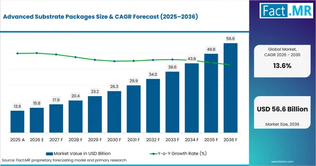
Advanced Substrate Packages Value Analysis | Source: Fact.MR
What are the defining numbers behind Advanced Substrate Packages Market growth?
An absolute opportunity of USD 40.8 billion is expected between 2026 and 2036.
- Demand Drivers in the Market
- AI system designers need wider memory interfaces and more die-to-die connections. The U.S. Department of Commerce finalized more than USD 1.4 billion in advanced-packaging awards in January 2025.
- Substrate producers are adding purpose-built capacity for server packages. Ibiden started construction of its Ono Plant in October 2025 for cutting-edge IC package substrates used in AI servers.
- Asian packaging clusters are funding pilot and volume capability. Taiwan's Ministry of Economic Affairs approved a NT$3.77 billion advanced R&D center in February 2026 with a 12-inch pilot line and packaging and testing functions.
- Key Segments Analyzed
- ABF organic substrates account for 39.0% of Substrate Type demand in 2026. ABF organic substrates lead because build-up films support fine routing, multiple redistribution layers and the body sizes required by server-class processors.
- FC-BGA represents 33.0% of the 2026 Package Architecture mix. FC-BGA remains the central volume architecture for large logic packages.
- The AI and data center segment captures 31.0% of End-use demand in 2026. AI and data centers pull the most substrate value because accelerators, CPUs, switches and high-bandwidth memory packages combine high pin counts with stringent signal and power requirements.
- Within Layer Count, 15-20 holds a 27.0% share in 2026. The 15-20 layer band balances routing density with manufacturability for mainstream high-performance packages.
- Analyst Opinion at Fact.MR
- Shambhu Nath Jha, Principal Consultant at Fact.MR, states, "Advanced substrates are now a system-performance decision. Buyers will reward suppliers that can hold fine-line yield while expanding body size and layer count. Capacity announcements matter, but proven qualification with accelerator, server and networking customers will determine who converts that capacity into durable revenue."
- Strategic Implications
- Substrate suppliers should reserve engineering capacity for co-design and warpage control, not only volume expansion. Samsung Electro-Mechanics described server and AI FC-BGA demand for additional layers and finer patterns in September 2025.
- Materials and equipment vendors should qualify glass and silicon-core routes alongside organic build-up systems. NIST's advanced-substrate awards support separate pilot paths for glass core, silicon core and fan-out packaging.
- European producers should tie capital spending to contracted technology ramps. AT&S indicated in May 2026 that IC-substrate demand had strengthened and planned roughly EUR 400 million of capital expenditure for fiscal 2026/27.
Japan's 15.9% CAGR through 2036 is tied to new IC-substrate capacity, while the USA reaches 15.3% as domestic packaging programs move into commercial execution. The UK is projected at 14.0% through specialist heterogeneous-integration work. Taiwan grows at 11.9% from a larger, mature packaging base, and South Korea at 10.9% on memory and server-package demand.
How does the Advanced Substrate Packages Market break down by segment?
ABF organic substrates, FC-BGA, AI and data center, and 15-20 layers
Which Substrate Type dominates?
ABF organic substrates: 39.0% share in 2026.
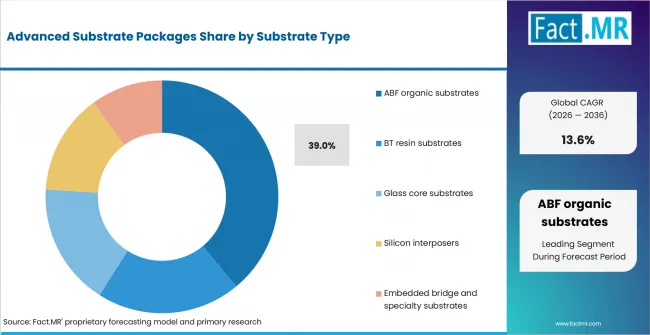
Advanced Substrate Packages Analysis By Substrate Type | Source: Fact.MR
ABF organic substrates lead because build-up films support fine routing, multiple redistribution layers and the body sizes required by server-class processors. They also fit established FC-BGA manufacturing flows, giving buyers a qualified route to higher I/O density.
What leads Package Architecture?
FC-BGA: 33.0% share in 2026.
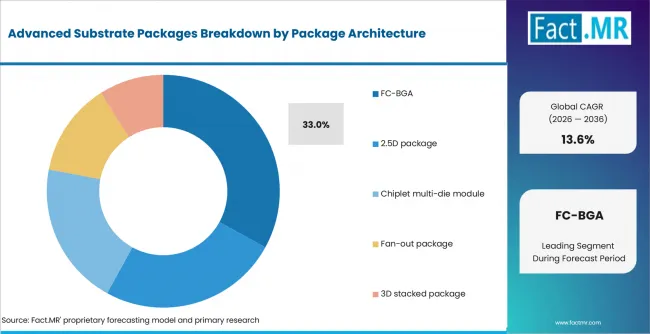
Advanced Substrate Packages Analysis By Package Architecture | Source: Fact.MR
FC-BGA remains the central volume architecture for large logic packages. Its substrate distributes power and high-speed signals between a fine-pitch die interface and a coarser board connection, a role that grows more demanding as package size and layer count increase.
Which End-use creates the strongest pull?
AI and data center: 31.0% share in 2026.
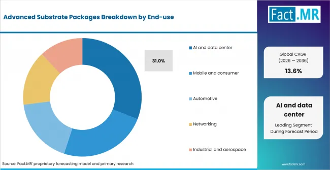
Advanced Substrate Packages Analysis By End Use | Source: Fact.MR
AI and data centers pull the most substrate value because accelerators, CPUs, switches and high-bandwidth memory packages combine high pin counts with stringent signal and power requirements. These programs also reward suppliers that can sustain yield during rapid design changes.
Why does the 15-20 layer band lead?
15-20: 27.0% share in 2026.
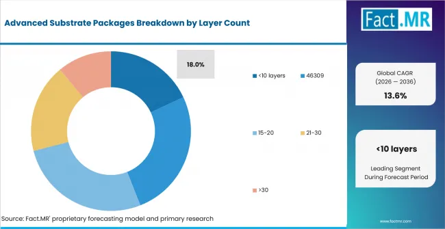
Advanced Substrate Packages Analysis By Layer Count | Source: Fact.MR
The 15-20 layer band balances routing density with manufacturability for mainstream high-performance packages. It accommodates added power and signal planes without moving every design into the cost and yield regime of the most complex stacks.
What is accelerating Advanced Substrate Packages Market adoption, and what is holding it back?
Demand is accelerating through AI compute, chiplet roadmaps and domestic packaging investment. Expansion remains exposed to substrate yield, long customer qualifications and the capital intensity of fine-line manufacturing.
Drivers Impact Analysis
| DRIVER | (~) % IMPACT ON CAGR | GEOGRAPHIC RELEVANCE | IMPACT TIMELINE |
|---|---|---|---|
| AI accelerators and high-bandwidth memory | +2.0% | USA, Taiwan, South Korea, Japan | Short term (<= 2 years) |
| Chiplet and heterogeneous integration | +1.5% | Global | Medium term (2-4 years) |
| Domestic advanced-packaging programs | +1.0% | USA, UK, Japan | Medium term (2-4 years) |
| Larger packages and higher layer counts | +0.8% | East Asia, North America | Long term (>= 4 years) |
- AI accelerators and high-bandwidth memory: More memory channels and wider die interfaces raise routing density and substrate value per package.
- Chiplet and heterogeneous integration: Multi-die systems shift interconnect work into substrates, bridges and interposers that must be co-designed with the package.
- Domestic advanced-packaging programs: Pilot lines and shared R&D infrastructure lower the entry barrier for materials, core and process innovation.
Opportunity Impact Analysis
| OPPORTUNITY | (~) % IMPACT ON CAGR | GEOGRAPHIC RELEVANCE | IMPACT TIMELINE |
|---|---|---|---|
| Glass-core and low-warpage substrates | +1.2% | USA, Japan, Taiwan | Medium term (2-4 years) |
| Co-design services for chiplet packages | +1.0% | Global | Short term (<= 2 years) |
| Specialist photonics and aerospace packages | +0.6% | UK, USA, Japan | Long term (>= 4 years) |
- Glass-core and low-warpage substrates: New core materials can improve dimensional stability for large packages, but suppliers must prove via formation, metallization and reliability at volume.
- Co-design services for chiplet packages: Substrate houses can deepen account value by joining power-delivery, signal-integrity and warpage decisions earlier in the design cycle.
- Specialist photonics and aerospace packages: Lower-volume programs offer entry points where domestic sourcing, thermal performance and traceability outweigh pure scale.
Restraints Impact Analysis
| RESTRAINT | (~) % IMPACT ON CAGR | GEOGRAPHIC RELEVANCE | IMPACT TIMELINE |
|---|---|---|---|
| Fine-line yield and warpage control | -0.9% | Global | Short term (<= 2 years) |
| Long platform qualification cycles | -0.7% | Global | Medium term (2-4 years) |
| High plant and process capital | -0.5% | USA, Europe, East Asia | Long term (>= 4 years) |
- Fine-line yield and warpage control: Larger bodies magnify alignment, flatness and thermal-expansion problems, so nominal capacity does not immediately become qualified output.
- Long platform qualification cycles: Server and automotive customers require reliability evidence across materials, process windows and multiple thermal conditions.
- High plant and process capital: Laser drilling, imaging, plating and inspection capacity must be installed as a balanced line, making partial expansions difficult to monetize.
Which countries are scaling the Advanced Substrate Packages Market through 2036?
- Japan sets the upper bound because new greenfield substrate lines add saleable capacity rather than only improving utilization.
- The USA is close behind as public funding moves glass, silicon-core and fan-out concepts toward domestic pilot production.
- The UK's design and compound-semiconductor base creates a specialist path into heterogeneous packages before mass-volume scale arrives.
- Taiwan's mature packaging ecosystem favors steady qualification-led expansion across foundry and OSAT customers.
- South Korea closes the set with strong technical demand but a more concentrated customer and supplier structure.
Qualification timelines, cluster maturity, package mix and available substrate capacity explain why the country trajectories differ. The wider report covers North America, Latin America, Western Europe, Eastern Europe, East Asia, South Asia & Pacific, Middle East & Africa.
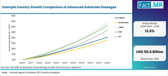
Example Country Growth Comparison Of Advanced Substrate Packages | Source: Fact.MR
| Country | CAGR (2026-2036) |
|---|---|
| Taiwan | 11.9% |
| South Korea | 10.9% |
| Japan | 15.9% |
| USA | 15.3% |
| UK | 14.0% |
What anchors Taiwan's demand?
11.9% CAGR, anchored by a dense packaging and testing cluster.
Taiwan converts design wins into substrate orders through a tightly connected foundry, packaging and testing base. The Ministry of Economic Affairs announced in November 2025 that ASE's K18B advanced packaging and testing project would involve NT$17.6 billion of investment. That cluster depth supports repeat demand for ABF build-up layers and fine-line routing, while qualification discipline keeps growth below the faster expansion expected in Japan and the USA.
How is South Korea developing demand?
10.9% CAGR, supported by memory, server and electronics supply chains.
South Korea's opportunity sits where memory, logic and substrate engineering meet. Samsung Electro-Mechanics stated in September 2025 that AI, cloud and server systems require FC-BGA designs with more layers and finer patterns. Local customers can co-develop high-density packages with electronics groups, although lengthy reliability testing and concentrated account structures temper the market's pace.
Why does Japan set the growth pace?
15.9% CAGR, led by fresh capacity for high-performance IC package substrates.
Japan combines specialist materials, precision process equipment and experienced substrate producers. Ibiden began work on its Ono Plant in October 2025 to serve rapidly expanding demand for cutting-edge IC package substrates used in AI servers. New lines can move the country beyond incremental debottlenecking, and that capacity-led reset gives Japan the highest displayed CAGR.
What supports the USA's expansion?
15.3% CAGR, backed by domestic advanced-packaging programs and AI system demand.
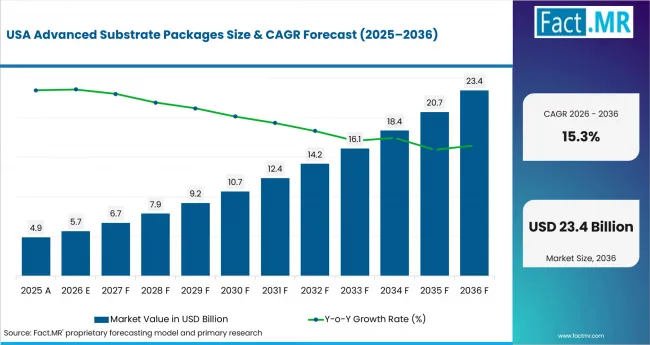
Advanced Substrate Packages Country Value Analysis | Source: Fact.MR
The USA is building a bridge between chip design leadership and domestic package manufacturing. The Department of Commerce finalized more than USD 1.4 billion in advanced-packaging awards in January 2025, while NIST-backed projects include glass-core, silicon-core and fan-out pilot capabilities. Procurement should concentrate on qualified domestic routes for AI accelerators, defense electronics and high-value networking hardware.
Where does the UK find its opening?
14.0% CAGR, supported by compound-semiconductor expertise and heterogeneous-integration policy.
The UK is approaching packaging as a route to capture more value from a design-heavy semiconductor base. Its National Semiconductor Strategy identifies advanced packaging and heterogeneous integration as capability priorities, and a 2026 sector study counted 703 semiconductor companies. Demand is likely to begin with R&D, photonics and specialist low-volume programs before wider manufacturing scale develops.
Who leads the Advanced Substrate Packages Market?
Ibiden, Shinko Electric Industries, Unimicron, AT&S, Samsung Electro-Mechanics and Kinsus.
Ibiden anchors the competitive discussion through high-performance IC package substrates and new capacity aimed at AI servers. Its advantage rests on fine-line process knowledge, customer qualification and the ability to scale complex layer structures.
Shinko Electric Industries and Unimicron bring established package-substrate portfolios across computing and communications. Shinko combines packaging process depth with substrate manufacturing, while Unimicron has broad Asian volume capability across advanced printed structures.
AT&S is strengthening its IC-substrate position through European and Asian manufacturing investment. Its route to share depends on ramp discipline, high-end customer programs and converting new capacity into qualified server output.
Samsung Electro-Mechanics participates through high-layer FC-BGA for servers, networks and automotive systems. Kinsus adds a Taiwan-based alternative with access to the region's semiconductor assembly ecosystem.
Competition turns on qualified yield, body-size capability, layer count and expansion timing. Buyers are likely to dual-source where package roadmaps expose them to one supplier's line or core-material constraint.
Which companies are the key providers?
Key companies include Ibiden; Shinko Electric Industries; Unimicron; AT&S; Samsung Electro-Mechanics; Kinsus.
- Ibiden
- Shinko Electric Industries
- Unimicron
- AT&S
- Samsung Electro-Mechanics
- Kinsus
Bibliography
- U.S. Department of Commerce. (2025, January 16). Biden-Harris Administration announces more than USD 1.4 billion in final awards to support next-generation semiconductor advanced packaging.
- National Institute of Standards and Technology. (2025, January 24). CHIPS National Advanced Packaging Manufacturing Program materials and substrates research and development awards.
- Ministry of Economic Affairs, Taiwan. (2026, February 11). Advanced semiconductor research and development center and 12-inch pilot line investment approval.
- Ministry of Economic Affairs, Taiwan. (2025, November 25). ASE K18B advanced packaging and testing investment.
- Department for Science, Innovation and Technology. (2023, May 19). National Semiconductor Strategy. UK Government.
- Department for Science, Innovation and Technology. (2026). UK semiconductor sector study.
- Ibiden Co., Ltd. (2025, October 10). Groundbreaking ceremony held for the new Ono Plant.
- Ibiden Co., Ltd. (2026). Top message and fiscal 2026 demand outlook.
- Samsung Electro-Mechanics. (2025, September 4). FC-BGA technology and demand for AI, cloud and server applications.
- AT&S. (2026, May 21). Annual results and fiscal 2026/27 capital expenditure outlook.
This Report Answers
- The report explains how advanced substrate packages demand is distributed across Substrate Type, Package Architecture, End-use and Layer Count.
- Segment analysis identifies the 2026 leaders and explains their purchase logic: Substrate Type: ABF organic substrates at 39.0%; Package Architecture: FC-BGA at 33.0%; End-use: AI and data center at 31.0%; Layer Count: 15-20 at 27.0%.
- The country section explains the distinct mechanisms shaping Taiwan, South Korea, Japan, USA and UK, focusing on semiconductor qualification, cluster maturity, package mix and available substrate capacity.
- Competitive analysis reviews current positions for Ibiden, Shinko Electric Industries, Unimicron, AT&S, Samsung Electro-Mechanics and Kinsus.
- Application analysis tests AI accelerators and high-bandwidth memory against the limiting effect of fine-line yield and warpage control.
What does the Advanced Substrate Packages Market cover?
Package substrates, interposers and embedded bridge structures that route power and high-speed signals among dies and between the package and printed circuit board in advanced semiconductor assemblies.
What is included in the scope?
The scope includes organic build-up substrates, glass-core substrates, silicon interposers and embedded bridge structures sold for FC-BGA, 2.5D, chiplet, fan-out and 3D package architectures. Revenue is attributed to the substrate or interconnect structure rather than the finished semiconductor device.
The boundary also considers through-glass via interposers and advanced packaging process-control software where those markets influence purchase timing but remain separately valued.
Coverage includes substrate design support and embedded passive or bridge features when sold as part of the package substrate. It also considers qualification activity that directly supports commercial substrate shipments across AI, mobile, automotive, networking and specialist electronics.
What is excluded from the scope?
The scope excludes bare semiconductor wafers, front-end fabrication revenue, finished processors, memory devices and general printed circuit boards. Packaging equipment and materials sold independently from the substrate are outside the market value.
Wire-bond leadframes, commodity laminate sheets and assembly or testing fees are excluded unless embedded in a priced advanced-substrate package. Research samples without a commercial supply path are not counted.
How Was the Analysis Built?
The analysis draws on 120+ sources, 35+ company portfolios, 25+ countries, and more than 20 industry interviews.
- Primary Research: Interviews cover manufacturers, technology developers, integrators, channel partners, end users and subject-matter experts relevant to this market. Discussions test purchase triggers, specification tradeoffs, implementation barriers, supplier positioning and the conditions required for wider commercial adoption.
- Desk Research: Research covers government statistics, regulatory publications, standards, company announcements, technical studies, trade information and industry associations. Published claims used in the analysis are documented in the bibliography.
- Market Sizing and Forecasting: The sizing model reconciles substrate area, layer complexity, package mix, qualified capacity and realized selling values across major architectures. Forecast weights reflect AI accelerator ramps, chiplet adoption, automotive qualification, plant additions and yield learning by country.
- Data Validation and Update Cycle: Findings are triangulated across interviews, public evidence, company activity, policy changes, trade patterns and implementation signals. Updates review product launches, capacity shifts, partnerships, approvals, procurement behavior and material changes in commercial adoption.
What is the report's scope and coverage?
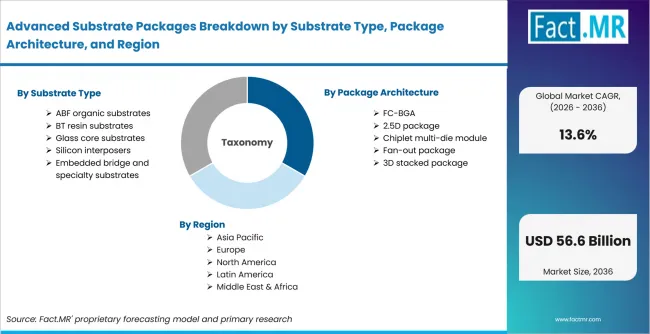
Advanced Substrate Packages Breakdown By Substrate Type, Package Architecture, And Region | Source: Fact.MR
| Attribute | Details |
|---|---|
| Quantitative Units | USD Billion |
| Market Definition | Package substrates, interposers and embedded bridge structures that route power and high-speed signals among dies and between the package and printed circuit board in advanced semiconductor assemblies. |
| Substrate Type | ABF organic substrates; BT resin substrates; Glass core substrates; Silicon interposers; Embedded bridge and specialty substrates |
| Package Architecture | FC-BGA; 2.5D package; Chiplet multi-die module; Fan-out package; 3D stacked package |
| End-use | AI and data center; Mobile and consumer; Automotive; Networking; Industrial and aerospace |
| Layer Count | <10 layers; 10-14; 15-20; 21-30; >30 |
| Regions Covered | North America; Latin America; Western Europe; Eastern Europe; East Asia; South Asia & Pacific; Middle East & Africa |
| Countries Covered | Taiwan; South Korea; Japan; USA; UK |
| Key Companies | Ibiden; Shinko Electric Industries; Unimicron; AT&S; Samsung Electro-Mechanics; Kinsus |
| Forecast Period | 2026 to 2036 |
| Approach | The sizing model reconciles substrate area, layer complexity, package mix, qualified capacity and realized selling values across major architectures. Forecast weights reflect AI accelerator ramps, chiplet adoption, automotive qualification, plant additions and yield learning by country. |
How is the market segmented?
-
By Substrate Type
- ABF organic substrates
- BT resin substrates
- Glass core substrates
- Silicon interposers
- Embedded bridge and specialty substrates
-
By Package Architecture
- FC-BGA
- 2.5D package
- Chiplet multi-die module
- Fan-out package
- 3D stacked package
-
By End-use
- AI and data center
- Mobile and consumer
- Automotive
- Networking
- Industrial and aerospace
-
By Layer Count
- <10 layers
- 10-14
- 15-20
- 21-30
- >30
-
By Region
- North America
- Latin America
- Western Europe
- Eastern Europe
- East Asia
- South Asia & Pacific
- Middle East & Africa