- Market Value (2025): USD 625.0 Mn
- Estimated Value (2026): USD 690.0 Mn
- Forecast Value (2036): USD 1850.0 Mn
- CAGR (2026-2036): 10.4%
What is the Deep Imaging Metrology Market forecast to be worth by 2036?
USD 690.0 million in 2026 to USD 1,850 million by 2036 at 10.4% CAGR.
- The deep imaging metrology market reached USD 625.0 million in 2025 as fab teams increased inspection around buried structures and high-aspect features.
- Demand is projected to increase from USD 690.0 million in 2026 to USD 1850.0 million by 2036.
- The market is forecast to record 10.4% CAGR from 2026 to 2036 as foundries, IDMs and memory makers tighten process-release checks.
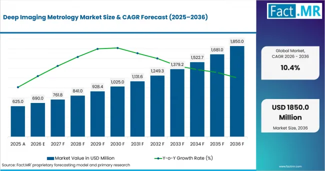
Deep Imaging Metrology Market Value Analysis | Source: Fact.MR
What are the defining numbers behind Deep Imaging Metrology Market growth?
USD 1.16 billion absolute opportunity by 2036, led by Optical CD imaging, Inline fab-integrated deployment and Foundries.
- Demand Drivers in the Market
- Foundry process teams need non-destructive imaging that confirms optical CD and buried-feature behavior before recipe sign-off. In January 2025, the U.S. Department of Commerce finalized USD 1.4 billion in CHIPS NAPMP awards for advanced packaging, including USD 1.1 billion for Natcast’s advanced packaging facility.
- Memory manufacturers need hybrid optical-SEM feedback so high-aspect structures can be measured before late-stage yield loss appears.
- IDM engineering groups use interferometric and scatterometry-fused imaging when electrical performance depends on small profile shifts.
- Research institutes rely on X-ray-assisted imaging when sub-surface structures cannot be evaluated through surface-only tools.
- Key Segments Analyzed
- By Imaging Modality: Optical CD imaging is expected to hold 34.0% share in 2026 because fabs already use CD signals for inline release.
- By Deployment: Inline fab-integrated tools are projected to account for 58.0% share in 2026 as fabs prefer measurement close to process chambers.
- By Node: Sub-3nm logic is anticipated to capture 31.0% share in 2026 due to tighter gate and interconnect tolerances.
- By End User: Foundries are estimated to represent 44.0% share in 2026 owing to high product mix and frequent process changes.
- By Structure Type: High-aspect-ratio structures are forecast to hold 38.0% share in 2026 since deep profiles need more than surface inspection.
- Analyst Opinion at Fact.MR
- Shambhu Nath Jha, Principal Consultant at Fact.MR states, “Deep imaging metrology is drawing attention because fab engineers need proof of buried geometry before release. Production acceptance is expected to depend on model validation and image correlation across real device stacks. Suppliers should combine optical speed, SEM confirmation and local application support.”
- Strategic Implications
- Fab engineering teams should define measurement-lineage rules before tool quotations move into purchasing.
- Equipment providers should prove reconstruction accuracy on real device stacks, not only calibration artifacts. In January 2025, CHIPS for America awarded USD 285 million to SMART USA for digital twins that aim to cut semiconductor development cycle times by 35% and manufacturing costs by more than 40%.
- Procurement leaders should compare service coverage and recipe-transfer support before selecting inline systems.
- Investors should separate deep imaging exposure from general inspection tools that do not reconstruct buried features.
The USA is projected to record 12.09% CAGR through 2036 with metrology validation work around advanced fabs. Taiwan is expected to post 12.05% CAGR as pilot-line capacity supports process checks. South Korea is forecast to reach 11.98% CAGR owing to memory and HBM qualification. Japan is anticipated to record 11.84% CAGR with equipment depth. China is estimated at 11.79% CAGR through IC output growth. Germany is projected to advance at 11.65% CAGR as specialty foundry projects expand.
How does the Deep Imaging Metrology Market break down by segment?
Optical CD imaging leads Imaging Modality at 34.0%; Inline fab-integrated deployment leads Deployment at 58.0%.
Which imaging modality leads?
Optical CD imaging is projected to account for 34.0% share in 2026.
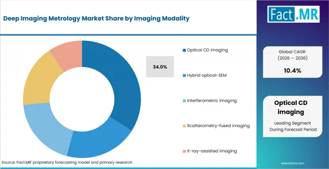
Deep Imaging Metrology Market Analysis By Imaging Modality | Source: Fact.MR
Optical CD imaging leads because semiconductor manufacturers widely integrate critical-dimension measurements into production workflows for rapid process monitoring. Its high throughput, established process compatibility, and reliable dimensional analysis support efficient process control across advanced semiconductor fabrication.
What leads the Deployment segment?
Inline fab-integrated tools are expected to hold 58.0% share in 2026.
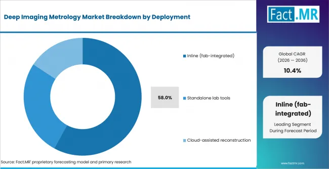
Deep Imaging Metrology Market Analysis By Deployment | Source: Fact.MR
Inline fab-integrated deployment leads because metrology results are available close to the production process, enabling faster inspection feedback and process adjustments. This approach supports continuous monitoring, improves manufacturing efficiency, and reduces delays in advanced semiconductor fabrication.
How does Node shape demand?
Sub-3nm logic is anticipated to lead with 31.0% share in 2026.
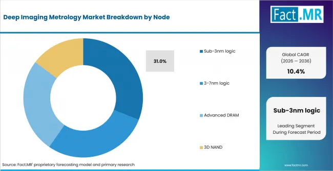
Deep Imaging Metrology Market Analysis By Node | Source: Fact.MR
Sub-3nm logic leads the node segment because shrinking transistor dimensions require highly precise imaging and process verification. Advanced metrology supports defect detection, dimensional accuracy, and tighter manufacturing control needed for next-generation semiconductor production.
Which End User leads?
Foundries are estimated to represent 44.0% share in 2026.
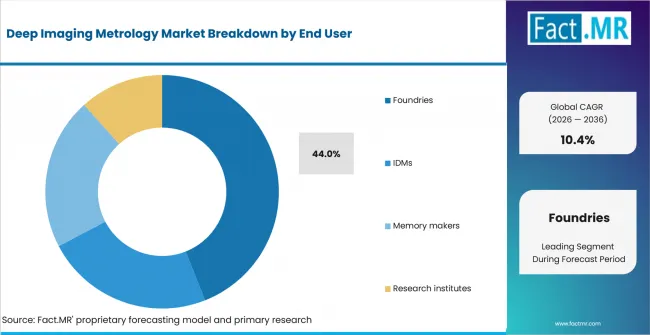
Deep Imaging Metrology Market Analysis By End User | Source: Fact.MR
Foundries lead the end-user segment because they manufacture diverse semiconductor products for multiple customers, requiring frequent process validation and inspection. Advanced metrology strengthens production consistency, defect analysis, and process optimization across leading-edge fabrication lines.
What supports High-aspect-ratio structures?
High-aspect-ratio structures are forecast to hold 38.0% share in 2026.
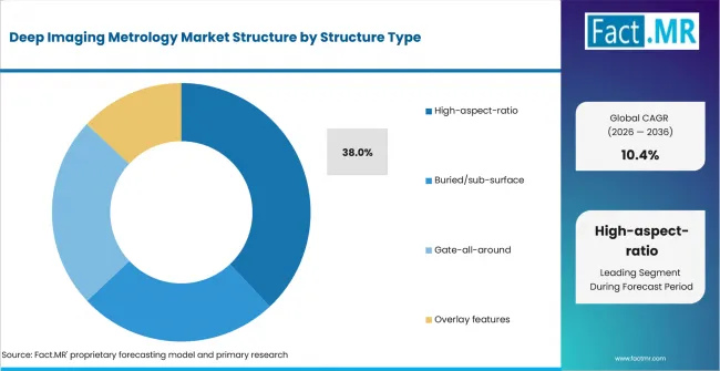
Deep Imaging Metrology Market Analysis By Structure Type | Source: Fact.MR
High-aspect-ratio structures lead because deep, narrow semiconductor features require detailed imaging beyond surface inspection. Advanced metrology improves visualization of complex geometries, supports accurate process verification, and helps manufacturers maintain yield and structural integrity in advanced device fabrication.
What is accelerating Deep Imaging Metrology Market adoption, and what is holding it back?
Deep-feature control accelerates adoption; reconstruction uncertainty restrains adoption.
Drivers Impact Analysis
| DRIVER | (~) % IMPACT ON CAGR | GEOGRAPHIC RELEVANCE | IMPACT TIMELINE |
|---|---|---|---|
| High-aspect-ratio profile control | +2.6% | USA, Taiwan, South Korea | Short term (<= 2 years) |
| Inline fab integration | +2.1% | USA, Taiwan, China | Short term (<= 2 years) |
| Buried-feature reconstruction | +1.8% | USA and Japan | Medium term (2-4 years) |
| GAA and HBM measurement depth | +1.4% | Taiwan, South Korea, Japan | Medium term (2-4 years) |
| Metrology model validation | +0.9% | USA, Germany | Long term (>= 4 years) |
- High-aspect-ratio profile control: Deep features are expected to raise demand for tools that measure sidewall shape and depth before yield loss appears. The need is sharper where optical CD data must be tied to hidden structure behavior.
- Inline fab integration: Fabs are projected to favor tools that return image-based results near the process step. Inline placement is expected to reduce delay between measurement, recipe adjustment and process release.
- Buried-feature reconstruction: Applied Materials introduced SEMVision H20 in February 2025 after advanced-node optical inspection began sending as much as 100X more defect candidates to eBeam review. That pressure is expected to support hybrid optical and SEM workflows.
- Metrology model validation: Measurement teams are expected to require test wafers and reference data before accepting a reconstruction model across production lines. Suppliers with traceable model outputs are expected to shorten approval discussions.
Opportunity Impact Analysis
| OPPORTUNITY | (~) % IMPACT ON CAGR | GEOGRAPHIC RELEVANCE | IMPACT TIMELINE |
|---|---|---|---|
| Hybrid optical-SEM workflows | +1.3% | USA, Japan, Taiwan | Medium term (2-4 years) |
| Cloud-assisted reconstruction | +1.0% | Global fabs with secure data flows | Medium term (2-4 years) |
| X-ray-assisted sub-surface imaging | +0.8% | Research and advanced packaging sites | Long term (>= 4 years) |
| Advanced packaging transfer | +0.7% | Taiwan, South Korea, Germany | Long term (>= 4 years) |
- Hybrid optical-SEM workflows: Suppliers can gain evaluation access when optical speed is paired with SEM detail for difficult structures. The workflow is expected to help fabs separate true buried defects from nuisance signals before release.
- Cloud-assisted reconstruction: Remote model processing is expected to help multi-fab groups reuse learning while keeping local release rules intact. Adoption is expected to depend on data handling terms and local application support.
- X-ray-assisted sub-surface imaging: X-ray methods are expected to support cases where buried features cannot be checked through top-side signals. The method is most useful when destructive sectioning is too slow for process-learning loops.
- Advanced packaging transfer: Nova released Nova WMC in August 2025 for advanced packaging metrology. The platform was designed for different wafer forms, high warpage and large-area nanometer-level mapping, which fits bonded and stacked structures.
Restraints Impact Analysis
| RESTRAINT | (~) % IMPACT ON CAGR | GEOGRAPHIC RELEVANCE | IMPACT TIMELINE |
|---|---|---|---|
| Reconstruction model uncertainty | -1.1% | Advanced-node fabs | Short term (<= 2 years) |
| Inline qualification time | -0.9% | Foundry and memory sites | Short term (<= 2 years) |
| Tool cost and service load | -0.7% | Smaller fabs and institutes | Medium term (2-4 years) |
| Export and data restrictions | -0.5% | China and cross-border fleets | Long term (>= 4 years) |
- Reconstruction model uncertainty: Fabs are expected to delay tool release when model outputs do not align with reference measurements. The problem is sharper for hidden structures because the measurement cannot be checked by routine surface inspection.
- Inline qualification time: Moving a tool into production requires recipe matching and control-plan work. Qualification effort is expected to stretch purchase cycles when model tuning depends on several process modules.
- Tool cost and service load: Smaller fabs are expected to limit adoption when utilization does not justify advanced optics and application support. Service access is expected to influence supplier choice more than tool speed alone.
- Export and data restrictions: Cross-border data rules can limit cloud reconstruction and remote support. Tool providers are expected to need local service models to reduce adoption risk.
Which countries are scaling Deep Imaging Metrology Market fastest?
USA 12.09%; Taiwan 12.05%; South Korea 11.98%; Japan 11.84%; Germany 11.65%.
- The country comparison spans 0.44 percentage points across the displayed forecast range.
- The USA remains 0.04 percentage point above Taiwan through metrology validation and advanced fab qualification.
- Taiwan remains 0.07 percentage point above South Korea as foundry scale supports pilot-line learning.
- South Korea remains 0.14 percentage point above Japan because memory makers keep qualification requirements strict.
- Japan remains 0.05 percentage point above China through imaging-tool capability and process engineering depth.
- China remains 0.14 percentage point above Germany as domestic IC output supports local metrology demand.
Comparable CAGRs create different entry conditions because fabs evaluate proof, service coverage and data handling in different ways. Full report coverage includes North America, Latin America, Europe, East Asia, South Asia and Pacific, and Middle East and Africa.
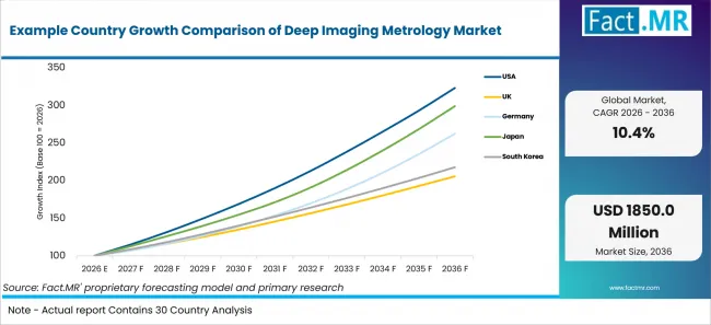
Example Country Growth Comparison Of Deep Imaging Metrology Market | Source: Fact.MR
| COUNTRY | CAGR |
|---|---|
| USA | 12.09% |
| Taiwan | 12.05% |
| South Korea | 11.98% |
| Japan | 11.84% |
| Germany | 11.65% |
What supports USA adoption?
12.09% CAGR, supported by metrology validation and advanced fab qualification.
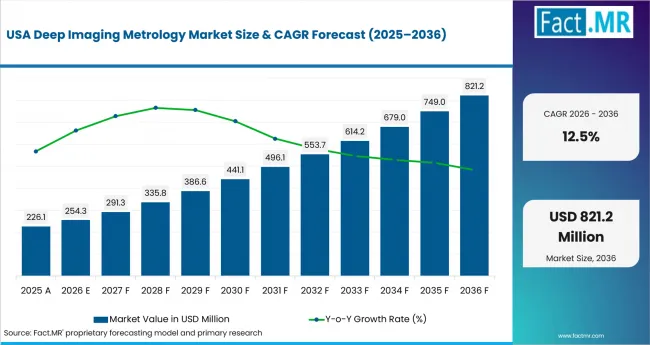
Deep Imaging Metrology Market Country Value Analysis | Source: Fact.MR
The USA accounts for 24.4% of 2026 demand. Adoption is tied to fabs that need non-destructive checks before process release and model sign-off. That work fits deep imaging metrology because reconstruction models must be trusted before fabs use them in production control.
How is Taiwan scaling demand?
12.05% CAGR, backed by foundry scale and pilot-line validation.
Taiwan accounts for 22.1% of 2026 demand. The Ministry of Economic Affairs announced in February 2026 that Taiwan’s first 12-inch advanced semiconductor pilot line would be built with NT$3.77 billion in investment. The same release said the facility aims to shorten product development cycles by about 30%. That setup is expected to support demand for optical CD imaging and hybrid optical-SEM validation close to foundry process work.
How is South Korea developing demand?
11.98% CAGR, driven by memory manufacturing and HBM qualification.
South Korea accounts for 19.1% of 2026 demand. Memory makers are expected to use deeper imaging checks before wide release of HBM and advanced DRAM processes. Local process teams also value rapid application support when optical models must be correlated with SEM evidence.
How does Japan perform?
11.84% CAGR, led by imaging-tool capability and process engineering depth.
Japan accounts for 14.6% of 2026 demand. That installed equipment base supports evaluation of interferometric imaging, optical CD tools and SEM-linked workflows. Japanese customers are expected to place weight on traceable measurement records during qualification.
How is Germany positioned?
11.65% CAGR, supported by specialized foundry and MEMS-related projects.
Germany accounts for 7.7% of 2026 demand. Specialty foundry and MEMS projects are expected to support demand for deep imaging metrology where process records must be traceable.
Who leads the Deep Imaging Metrology Market?
KLA and Applied Materials show direct relevance in process control. Onto Innovation and Nova extend optical metrology coverage. Hitachi High-Tech and Bruker broaden SEM and nanoscale metrology capability.
KLA supports the market through semiconductor process-control systems that combine inspection, metrology and data analytics. Applied Materials contributes eBeam defect review for image-based release decisions. Onto Innovation and Nova provide optical metrology platforms for logic, memory and packaging workflows. Hitachi High-Tech strengthens SEM-based imaging depth. Bruker adds AFM and nanoscale metrology capability.
Which companies are the key providers?
Key companies include KLA Corporation, Applied Materials, Inc., Onto Innovation Inc., Nova Ltd., Hitachi High-Tech Corporation, and Bruker Corporation.
- KLA Corporation
- Applied Materials, Inc.
- Onto Innovation Inc.
- Nova Ltd.
- Hitachi High-Tech Corporation
- Bruker Corporation
Bibliography
- Applied Materials, Inc. (2025, February 19). Applied Materials accelerates chip defect review with next-gen eBeam system.
- European Commission. (2025, December 11). Commission approves €623 million German State aid to support set-up of two first-of-a-kind chips factories in Germany.
- Department of Industrial Technology, Ministry of Economic Affairs. (2026, February 11). MOEA breaks ground on Advanced Semiconductor R&D Center: Taiwan’s first 12-inch pilot line to target AI, silicon photonics, and quantum technology.
- National Institute of Standards and Technology. (2025, April 25). NIST study aims to improve utility of the scanning electron microscope.
- Nova Ltd. (2025, August 26). Nova announces the release of Nova WMC: A next-generation modular optical metrology platform for advanced packaging.
- Onto Innovation Inc. (2025, September 9). Onto Innovation launches next generation OCD metrology platform to enable process control for advanced AI devices.
- Ministry of Economy and Finance. (2025, March 5). A 50 trillion KRW high-tech strategic industry fund to be established.
- Semiconductor Equipment Association of Japan. (2026, April 8). SEAJ reports 2025 worldwide semiconductor equipment billings US$135.1 billion.
- Bruker Corporation. (2025, June 24). Bruker experiences growth in semiconductor advanced packaging market fueled by AI demands.
This Report Answers
- The report provides strategic intelligence on the Deep Imaging Metrology Market across Imaging Modality and Deployment choices that shape semiconductor process-control programs.
- Segment analysis covers Optical CD imaging and Inline fab-integrated deployment as the share leaders within the 2026 market.
- Country outlook evaluates the USA and Taiwan alongside South Korea and Japan. China and Germany complete the growth comparison across the profiled markets.
- Competitive analysis profiles KLA and Applied Materials alongside Onto Innovation and Nova. Hitachi High-Tech and Bruker complete the provider set across optical, SEM and nanoscale metrology.
- Structure analysis covers High-aspect-ratio and Buried/sub-surface features.
- Automation context is considered only where semiconductor robot systems move wafers into measurement steps.
What does the Deep Imaging Metrology Market cover?
Deep imaging metrology systems measure semiconductor structures where surface inspection is not enough. They support release decisions when fabs must confirm hidden geometry without cutting wafers.
The Deep Imaging Metrology Market covers optical CD imaging and hybrid optical-SEM workflows. It also includes interferometric, scatterometry-fused and X-ray-assisted imaging where sub-surface measurement supports process control.
What is included in the scope?
The scope includes Imaging Modality and Deployment alongside Node, End User and Structure Type. Foundries, IDMs, memory makers and research institutes are included when imaging metrology supports process release or recipe qualification.
What is excluded from the scope?
General inspection tools remain outside the scope when they do not reconstruct deep or buried semiconductor geometry.
The scope excludes routine surface inspection, film-thickness tools and lab microscopes without fab metrology use. General packaging equipment is excluded unless demand depends on deep image-based measurement.
How Was the Analysis Built?
The analysis draws on 120+ sources, 35+ company portfolios, 25+ countries and more than 20 industry interviews.
- Primary Research: Primary research includes discussions with manufacturers and service providers. It also covers technology developers, end users and procurement teams. These conversations examine adoption, approval requirements and market acceptance.
- Desk Research: Desk research covers government statistics, regulatory publications and company filings. It also reviews technical studies, standards and public policy. Each source used in the analysis is documented in the bibliography.
- Market Sizing and Forecasting: Market estimates combine historical performance, demand indicators and segment shares. They also review company participation, country growth and adoption barriers.
- Data Validation and Update Cycle: Findings are validated against public data, company activity, regulatory changes and industry developments. Updates review product launches, capacity changes and shifts in commercial adoption.
What is the report’s scope and coverage?
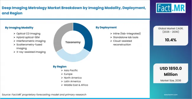
Deep Imaging Metrology Market Breakdown By Imaging Modality, Deployment, And Region | Source: Fact.MR
| ATTRIBUTE | DETAILS |
|---|---|
| Quantitative Units | USD Million |
| Market Definition | Semiconductor imaging metrology systems used to reconstruct optical CD, buried geometry, high-aspect profiles and sub-surface features where process release depends on non-destructive image evidence |
| Imaging Modality | Optical CD imaging; Hybrid optical-SEM; Interferometric imaging; Scatterometry-fused imaging; X-ray-assisted imaging |
| Deployment | Inline fab-integrated; Standalone lab tools; Cloud-assisted reconstruction |
| Node | Sub-3nm logic; 3-7nm logic; Advanced DRAM; 3D NAND |
| End User | Foundries; IDMs; Memory makers; Research institutes |
| Structure Type | High-aspect-ratio; Buried/sub-surface; Gate-all-around; Overlay features |
| Regions Covered | North America; Latin America; Europe; East Asia; South Asia and Pacific; Middle East and Africa |
| Countries Covered | USA; Taiwan; South Korea; Japan; China; Germany |
| Companies Profiled | KLA Corporation; Applied Materials, Inc.; Onto Innovation Inc.; Nova Ltd.; Hitachi High-Tech Corporation; Bruker Corporation |
| Forecast Period | 2026 to 2036 |
| Approach | Hybrid top-down and bottom-up approach using semiconductor equipment demand, process-control requirements, advanced-node adoption, deep-feature inspection needs, country adoption patterns and company portfolio review |
How is the market segmented?
-
By Imaging Modality:
- Optical CD imaging
- Hybrid optical-SEM
- Interferometric imaging
- Scatterometry-fused imaging
- X-ray-assisted imaging
-
By Deployment:
- Inline fab-integrated
- Standalone lab tools
- Cloud-assisted reconstruction
-
By Node:
- Sub-3nm logic
- 3-7nm logic
- Advanced DRAM
- 3D NAND
-
By End User:
- Foundries
- IDMs
- Memory makers
- Research institutes
-
By Structure Type:
- High-aspect-ratio
- Buried/sub-surface
- Gate-all-around
- Overlay features
-
By Region:
- North America
- Latin America
- Western Europe
- Eastern Europe
- East Asia
- South Asia and Pacific
- Middle East & Africa