- Market Value (2025): USD 190.6 Mn
- Estimated Value (2026): USD 224.0 Mn
- Forecast Value (2036): USD 1120.0 Mn
- CAGR (2026-2036): 17.5%
What is the Glass Core Via Tools Market forecast to be worth by 2036?
USD 224.0 million in 2026 to USD 1,120.0 million by 2036, at a 17.5% CAGR.
- The Glass Core Via Tools Market crossed a valuation of USD 190.6 million in 2025, supported by demand from Substrate manufacturers serving Glass core substrates workflows that require forming dense through-glass vias with controlled taper and minimal cracking in a brittle, electrically insulating substrate.
- Demand is projected to increase from USD 224.0 million in 2026 to USD 1,120.0 million by 2036.
- The market is forecast to record a 17.5% CAGR from 2026 to 2036 as uv laser drilling (355/532 nm), lide and electrochemical discharge machining remain central purchase reasons.
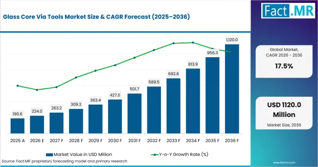
Glass Core Via Tools Market Value Analysis | Source: Fact.MR
What are the defining numbers behind Glass Core Via Tools Market growth?
USD 896.0 million absolute opportunity is expected by 2036.
- Demand Drivers in the Market
- UV laser drilling (355/532 nm): UV laser drilling remains the workhorse process for larger-geometry vias, delivering 30-100 micrometer vias at up to 10:1 aspect ratio and pitches of 100 micrometers or wider, giving buyers a proven, lower-cost route wherever the panel design does not need the tightest pitch.
- LIDE: Demand is shifting toward laser-induced deep etching as pitch tightens below 80 micrometers, because LIDE reaches 10-50 micrometer vias at up to 20:1 aspect ratio with smooth sidewalls, and laser-modified zones etch up to 100 times faster than unmodified glass in HF or hot alkaline etchant - a speed advantage that directly improves tool throughput and cost per via.
- Electrochemical discharge machining: Electrochemical discharge machining is carving out a defined niche in power and ground via formation, where its 50-200 micrometer vias at roughly 5:1 aspect ratio are well matched to lower-precision, higher-current paths that do not need LIDE-class geometry. [2][3]
- State-of-the-art design rules: Toolmakers are being pulled toward tighter design rules as roadmaps advance: production lines are already running 50 micrometer vias at 80 micrometer pitch, 8:1 aspect ratio, and plus-or-minus 5 micrometer registration on 100-500 micrometer glass, while research lines are demonstrating 10 micrometer vias at 40 micrometer pitch, 20:1 aspect ratio, and via densities of 10,000 per square centimeter - a preview of the specs equipment will need to hit as the roadmap matures. [2]
- Key Segments Analyzed
- By Via Formation Method: Laser-induced deep etching is projected to hold 34.0% share in 2026, supported by a clear process advantage: Laser-induced deep etching modifies selected volumes inside the glass and then removes them chemically, enabling small vias with less molten debris than direct ablation. The separation of modification and material removal also supports tapered or shaped profiles.
- By Via Geometry: <20 um diameter is projected to hold 44.0% share in 2026, supported by a clear process advantage: Diameters below 20 micrometers support the I/O density needed for advanced package substrates and glass interposers. They also raise the aspect ratio and make sidewall quality, taper and downstream seed coverage decisive.
- By Glass Thickness: <300 um is projected to hold 39.8% share in 2026, supported by a clear process advantage: Glass below 300 micrometers shortens the via path, reduces etch or drilling time and makes conformal metallization easier. It also supports thinner package structures where glass is chosen for dimensional stability.
- By Application: Glass core substrates are projected to hold 41.1% share in 2026, supported by a clear process advantage: Glass core substrates require via formation as a foundational manufacturing step rather than an optional feature. The via tool determines whether the low-warpage glass panel can be converted into a routable package core.
- By End User: Substrate manufacturers are projected to hold 30.7% share in 2026, supported by a clear process advantage: Substrate manufacturers own the sequence from glass panel preparation through via formation, metallization and redistribution. Their yield is determined by how well the via process transfers into later plating and lamination steps.
- Analyst Opinion at Fact.MR
- Shambhu Nath Jha, Sr. Consultant at Fact.MR, states, 'Buyers should evaluate the complete process sequence around forming dense through-glass vias with controlled taper and minimal cracking in a brittle, electrically insulating substrate. Technical review should focus on repeatability, integration, defect control and production throughput rather than a single headline specification. Suppliers that connect tool performance to measurable yield and qualification results are likely to build trust faster.'
- Strategic Implications
- The process should be qualified together with downstream metallization because sidewall damage and taper determine seed continuity and fill yield.
- Equipment suppliers should document how their systems address the challenge of forming dense through-glass vias with controlled taper and minimal cracking in a brittle, electrically insulating substrate across production-representative wafers, panels, dies or packages.
- Procurement teams should compare glass-core via formation accuracy, drill or laser throughput, via-wall integrity, panel handling, metallization compatibility and qualification support for advanced packaging lines.
Japan is projected to record a 17.8% CAGR as semiconductor equipment, materials, inspection and memory-process expertise supports relevant capital spending; South Korea is projected to record a 18.5% CAGR as high-volume memory, HBM and vertically integrated semiconductor manufacturing supports relevant capital spending; Taiwan is projected to record a 18.6% CAGR as leading foundry production, advanced packaging and a dense OSAT and substrate supply chain supports relevant capital spending; Austria is projected to record a 16.8% CAGR as European wafer-bonding and substrate-equipment expertise, including a strong advanced-packaging supplier base supports relevant capital spending; while USA is projected to record a 18.9% CAGR as leading-edge logic, high-performance computing, federally supported semiconductor R&D and a large domestic equipment base supports relevant capital spending through 2036.
How does the Glass Core Via Tools Market break down by segment?
Laser-induced deep etching leads Via Formation Method with a 34.0% share, while <20 um diameter accounts for 44.0% of Via Geometry in 2026.
Why does Laser-induced deep etching lead Via Formation Method?
Laser-induced deep etching is projected to account for 34.0% share in 2026.
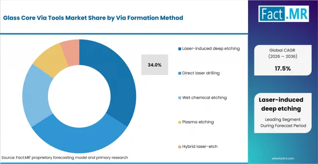
Glass Core Via Tools Market Analysis By Via Formation Method | Source: Fact.MR
Laser-induced deep etching modifies selected volumes inside the glass and then removes them chemically, enabling small vias with less molten debris than direct ablation. The separation of modification and material removal also supports tapered or shaped profiles. Direct laser drilling is simpler and fast for larger holes, but thermal damage, debris and microcracking become harder to manage as diameter falls. Of TGV formation: laser ablation issues (heat-affected zone, protrusions impeding bonding) and mitigations (organic overlayer, liquid immersion cooling, preheating, shorter pulses); LIDE induced zones ~1 µm diameter, arbitrary via shapes via 1-10 µm connected vias. [7] Buyers therefore tend to treat laser-induced deep etching as the practical choice when qualification must balance process capability, repeatability and production economics.
Why does <20 um diameter lead Via Geometry?
<20 um diameter is projected to account for 44.0% share in 2026.
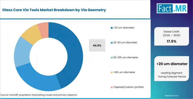
Glass Core Via Tools Market Analysis By Via Geometry | Source: Fact.MR
Diameters below 20 micrometers support the I/O density needed for advanced package substrates and glass interposers. They also raise the aspect ratio and make sidewall quality, taper and downstream seed coverage decisive. The 20-50 micrometer range is easier to drill and metallize but delivers lower routing density. Production 50 µm via / 80 µm pitch / 8:1 AR / ±5 µm registration on 100-500 µm glass; research 10 µm via / 40 µm pitch / 20:1 AR / 10,000 vias/cm². [2] Buyers therefore tend to treat <20 um diameter as the practical choice when qualification must balance process capability, repeatability and production economics.
Why does <300 um lead Glass Thickness?
<300 um is projected to account for 39.8% share in 2026.
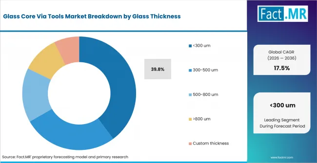
Glass Core Via Tools Market Analysis By Glass Thickness | Source: Fact.MR
Glass below 300 micrometers shortens the via path, reduces etch or drilling time and makes conformal metallization easier. It also supports thinner package structures where glass is chosen for dimensional stability. Thicker glass improves stiffness and handling, but it raises aspect ratio, process time and the probability of incomplete sidewall coverage. 10-50 Μm vias, up to 20:1 aspect ratio, <80 µm pitch, smooth sidewalls; laser-modified zones etch up to 100× faster than unmodified glass in HF or hot alkaline etchant. Buyers therefore tend to treat <300 um as the practical choice when qualification must balance process capability, repeatability and production economics.
Why do Glass core substrates lead Application?
Glass core substrates are projected to account for 41.1% share in 2026.
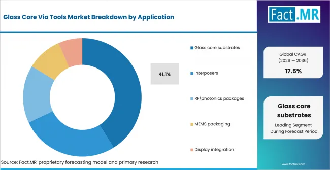
Glass Core Via Tools Market Analysis By Application | Source: Fact.MR
Glass core substrates require via formation as a foundational manufacturing step rather than an optional feature. The via tool determines whether the low-warpage glass panel can be converted into a routable package core. Interposers use similar processes, but glass-core manufacturing represents the broadest direct equipment pull across large substrate panels. Absolics received up to $75M direct funding (finalized Dec 2024) plus a $100M R&D award (Dec 2024) with Georgia Tech's 3D Packaging Research Center for glass core substrates - the anchor US policy bet on this tool chain. [10][11] Buyers therefore tend to treat glass core substrates as the practical choice when qualification must balance process capability, repeatability and production economics.
Why do Substrate manufacturers lead End User?
Substrate manufacturers are projected to account for 30.7% share in 2026.
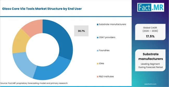
Glass Core Via Tools Market Analysis By End User | Source: Fact.MR
Substrate manufacturers own the sequence from glass panel preparation through via formation, metallization and redistribution. Their yield is determined by how well the via process transfers into later plating and lamination steps. OSAT providers consume finished substrates and may influence specifications, but the via-formation capital is concentrated upstream at substrate makers. Intel demonstrated a thick-core glass substrate with EMIB (78×77 mm package) at NEPCON Japan (Jan 2026); TSMC pulled its CoPoS panel pilot line to mid-2026 with volume 2028-29; Absolics completed major equipment install in Georgia and began mass-production sampling to AMD (Jan 2026). [8] Buyers therefore tend to treat substrate manufacturers as the practical choice when qualification must balance process capability, repeatability and production economics.
What is accelerating Glass Core Via Tools Market adoption, and what is holding it back?
The strongest accelerator is UV laser drilling (355/532 nm), while the main restraint is that glass fracture, debris, slow etch kinetics and panel handling can erase the dimensional-stability benefit of the substrate.
Drivers Impact Analysis
| DRIVER | MARKET RELEVANCE | PRIMARY ADOPTION CONTEXT | RELEVANCE HORIZON |
|---|---|---|---|
| UV laser drilling (355/532 nm) | High | Global leading-edge fabs | 2026 to 2036 |
| LIDE | High | Global leading-edge fabs | 2026 to 2036 |
| Electrochemical discharge machining | High | Global leading-edge fabs | 2026 to 2036 |
| State-of-the-art design rules | High | Global leading-edge fabs | Short term (<=2 years) |
Source: Fact.MR analysis. Updated Jul 23, 2026
- UV laser drilling (355/532 nm): 30-100 Μm vias, up to 10:1 aspect ratio, at least 100 µm pitch.
- LIDE: 10-50 Μm vias, up to 20:1 aspect ratio, <80 µm pitch, smooth sidewalls; laser-modified zones etch up to 100× faster than unmodified glass in HF or hot alkaline etchant.
- Electrochemical discharge machining: 50-200 Μm vias, 5:1, suited to power/ground vias. [2][3]
- State-of-the-art design rules: Production 50 µm via / 80 µm pitch / 8:1 AR / ±5 µm registration on 100-500 µm glass; research 10 µm via / 40 µm pitch / 20:1 AR / 10,000 vias/cm². [2]
Opportunity Impact Analysis
| OPPORTUNITY | MARKET RELEVANCE | PRIMARY ADOPTION CONTEXT | RELEVANCE HORIZON |
|---|---|---|---|
| Panel-scale qualification (2025-2026 inflection) | High | Japan | Short term (<=2 years) |
| NEG dual-track glass | High | Global leading-edge fabs | Short term (<=2 years) |
| Inspection co-development | High | Global leading-edge fabs | 2026 to 2036 |
Source: Fact.MR analysis. Updated Jul 23, 2026
- Panel-scale qualification (2025-2026 inflection): Intel demonstrated a thick-core glass substrate with EMIB (78×77 mm package) at NEPCON Japan (Jan 2026); TSMC pulled its CoPoS panel pilot line to mid-2026 with volume 2028-29; Absolics completed major equipment install in Georgia and began mass-production sampling to AMD (Jan 2026). [8]
- NEG dual-track glass: Nippon Electric Glass shipped 515×510 mm TGV substrate samples for both laser-modification/etch (0.4 mm thick, φ50 µm) and CO2 laser processing (0.5 mm, φ90 µm), targeting mass production by 2028. [9]
- Inspection co-development: Onto Innovation frames TGV metrology (via shape, cracks, CD across panels) as a gating item for HVM - via tools are being co-specified with metrology. [3]
Restraints Impact Analysis
| RESTRAINT | MARKET RELEVANCE | PRIMARY ADOPTION CONTEXT | RELEVANCE HORIZON |
|---|---|---|---|
| Primary qualification constraint | High | Global leading-edge fabs | 2026 to 2036 |
| Buried-defect escape | High | Global leading-edge fabs | 2026 to 2036 |
| Buried-defect escape | High | Global leading-edge fabs | 2026 to 2036 |
Source: Fact.MR analysis. Updated Jul 23, 2026
- Primary qualification constraint: Glass fracture, debris, slow etch kinetics and panel handling can erase the dimensional-stability benefit of the substrate. [4]
- Buried-defect escape: CO2 laser (9-11 µm) drilling is fast and PCB-compatible but thermally stressed (mitigated by pattern design + anneal); excimer (193-351 nm) minimizes thermal damage at the cost of speed; femtosecond/picosecond laser-modification + wet etch creates nano-void modified zones with high etch selectivity - non-scanning methods (filamentation, diffractive optics) modify glass with a single pulse for higher productivity. [4]
- Buried-defect escape: Peer-reviewed ultrashort-pulse laser drilling in 200 µm Borofloat 33 achieved 7.3±0.1° taper with 5 ps / 25 µJ / 600 passes at 125 µm diameter, 180 µm minimum pitch, no cracks after thermal cycling/shock to 950 °C, and 37.4% reduction of laser-induced stress (to 8.2 MPa) with a multi-path rotating-start scanning strategy. [5]
Which countries are scaling Glass Core Via Tools Market fastest?
For Glass Core Via Tools Market, South Korea's 18.5% CAGR reflects high-volume memory, HBM and vertically integrated semiconductor manufacturing.
- Countries differ less by the headline CAGR than by the type of semiconductor work creating demand for the Glass Core Via Tools Market.
- China demand is linked to domestic packaging capacity, local-tool development and access constraints, while USA demand is associated with advanced packaging programs, glass-substrate research and equipment qualification.
- Taiwan is driven by foundry and OSAT integration, whereas South Korea combines memory, HBM and advanced-packaging investment.
- Japan contributes precision equipment and materials capability, while Austria is linked to European substrate, bonding and advanced-packaging supply chains.
- Country forecasts reflect aggregate packaging demand. Glass-core substrate programs, panel processing capability, equipment supply, export controls and qualification cycles shape local adoption conditions.
The six profiled markets are evaluated against wider activity in North America, Latin America, Europe, East Asia, South Asia & Oceania, and the Middle East & Africa.
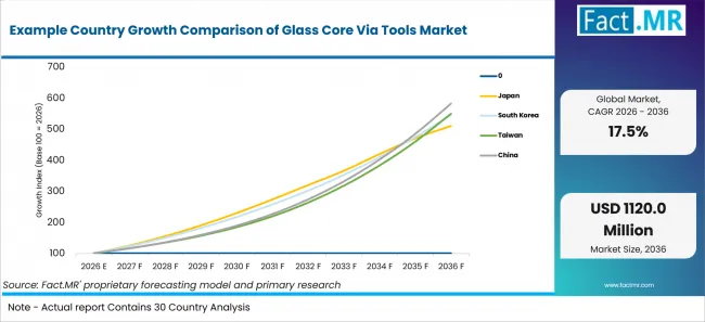
Example Country Growth Comparison Of Glass Core Via Tools Market | Source: Fact.MR
| COUNTRY | CAGR, 2026 to 2036 |
|---|---|
| USA | 18.9% |
| Taiwan | 18.6% |
| South Korea | 18.5% |
| Japan | 17.8% |
| Austria | 16.8% |
Source: Fact.MR analysis. Updated Jul 23, 2026
What is driving USA's growth through 2036?
18.9% CAGR from 2026 to 2036. Local leading-edge logic, high-performance computing, federally supported semiconductor R&D and a large domestic equipment base.
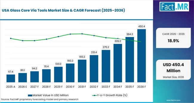
Glass Core Via Tools Market Country Value Analysis | Source: Fact.MR
What is driving Taiwan's growth through 2036?
18.6% CAGR from 2026 to 2036. Local leading foundry production, advanced packaging and a dense OSAT and substrate supply chain.
Taiwan combines leading foundry production, advanced packaging and a dense OSAT and substrate supply chain with a 19.3% share of 2026 demand across the six profiled countries. Onto Innovation frames TGV metrology (via shape, cracks, CD across panels) as a gating item for HVM - via tools are being co-specified with metrology. [3] The commercial link is the need to solve the problem of forming dense through-glass vias with controlled taper and minimal cracking in a brittle, electrically insulating substrate as capacity and process complexity increase.
What is driving South Korea's growth through 2036?
18.5% CAGR from 2026 to 2036. Local high-volume memory, HBM and vertically integrated semiconductor manufacturing.
What is driving Japan's growth through 2036?
17.8% CAGR from 2026 to 2036. Local semiconductor equipment, materials, inspection and memory-process expertise.
AGC (IEEE chapter author), NEG - materials-led; RENA/LPKF supply process tools (Germany). This environment creates a clear qualification pathway for the Glass Core Via Tools Market because buyers must solve the problem of forming dense through-glass vias with controlled taper and minimal cracking in a brittle, electrically insulating substrate at production scale.
What is driving Austria's growth through 2036?
16.8% CAGR from 2026 to 2036. Local European wafer-bonding and substrate-equipment expertise, including a strong advanced-packaging supplier base.
Austria combines European wafer-bonding and substrate-equipment expertise, including a strong advanced-packaging supplier base with a 11.9% share of 2026 demand across the six profiled countries. 50-200 Μm vias, 5:1, suited to power/ground vias. [2][3] The commercial link is the need to solve the problem of forming dense through-glass vias with controlled taper and minimal cracking in a brittle, electrically insulating substrate as capacity and process complexity increase.
Who leads the Glass Core Via Tools Market?
LPKF Laser & Electronics and Corning lead the competitive landscape, followed by Applied Materials and Schott as the next tier of challengers.
LPKF Laser & Electronics participates through laser-based glass microvia formation, with relevance determined by its ability to address the challenge of forming dense through-glass vias with controlled taper and minimal cracking in a brittle, electrically insulating substrate. Corning participates through engineered glass substrates and materials development, with relevance determined by its ability to address the challenge of forming dense through-glass vias with controlled taper and minimal cracking in a brittle, electrically insulating substrate. Applied Materials participates through deposition, etch, materials engineering and integrated process modules, with relevance determined by its ability to address the challenge of forming dense through-glass vias with controlled taper and minimal cracking in a brittle, electrically insulating substrate. Schott participates through specialty glass materials and substrates, with relevance determined by its ability to address the challenge of forming dense through-glass vias with controlled taper and minimal cracking in a brittle, electrically insulating substrate.
Via Mechanics holds a more specialized role through laser drilling and substrate-processing equipment, particularly where custom integration and service coverage affect qualification. Disco holds a more specialized role through dicing, grinding and precision wafer processing, particularly where custom integration and service coverage affect qualification.
Competition is expected to center on repeatable process performance, integration with adjacent modules, installed-base service and documented capability to address the challenge of forming dense through-glass vias with controlled taper and minimal cracking in a brittle, electrically insulating substrate. Buyers are likely to compare accuracy, defect prevention, throughput, recipe stability and the completeness of the delivered process cell.
Which companies are the key providers?
Key companies include LPKF Laser & Electronics; Corning; Applied Materials; Schott; Via Mechanics; Disco.
- LPKF Laser & Electronics
- Corning
- Applied Materials
- Schott
- Via Mechanics
- Disco
Bibliography
- [2] Onto Innovation. (n.d.). Through The Glass Why The Rapid Development Of Tgv Demands Rigorous Analysis.
- [3] Eps. (n.d.). Glass Substrates Adv Substrates Tc Updated Nov25.
- [4] Sciencedirect. (n.d.). S014381662500291X.
- [5] MDPI. (n.d.). 171.
- [7] Nippon Electric Glass. (n.d.). 1.
- [8] Absolics. (n.d.). Official website or source page.
- [9] Grokipedia. (n.d.). Absolics.
- [10] Koreaherald. (n.d.). Source document.
- [11] Trendforce. (n.d.). News Korea Challenges Intel On Glass Substrate Standards As Absolics Samsung Accelerate Commercialization.
This Report Addresses
- The report provides strategic intelligence on Glass Core Via Tools Market across Via Formation Method and Via Geometry choices that shape purchasing decisions.
- Segment analysis covers Laser-induced deep etching as the share leader within the 2026 market structure.
- Regional outlook evaluates Japan and South Korea alongside Taiwan while Austria and USA complete the growth comparison.
- Competitive analysis profiles LPKF Laser & Electronics and Corning alongside Applied Materials and Schott, followed by additional active providers.
- Use-case assessment covers the categories and applications that shape demand in the Glass Core Via Tools Market across the forecast period.
What does the Glass Core Via Tools Market cover?
The market covers equipment and process systems configured to address the challenge of forming dense through-glass vias with controlled taper and minimal cracking in a brittle, electrically insulating substrate.
Glass core via tools are the laser and etch systems that form through-glass vias (TGVs) in glass core substrates for advanced packaging: UV/CO2/excimer/ultrashort-pulse laser drilling, and laser-induced deep etching (LIDE) platforms combining femtosecond/picosecond laser modification with selective wet etch. This is a distinct equipment category from PCB drilling - specs target <100 µm pitch, high aspect ratio, and zero microcracks on 100-500 µm glass at panel sizes (510×515 mm, 600×600 mm).
Commercial value includes glass-core via drilling or laser tools, panel handling, alignment, inspection, process-control software and application support. Finished devices, package value and unrelated semiconductor equipment are excluded.
What is included in the scope?
The scope includes systems used by substrate manufacturers and the other end-user groups listed in the segmentation.
The market is segmented by Via Formation Method, including Laser-induced deep etching, Direct laser drilling, Wet chemical etching, Plasma etching, Hybrid laser-etch; Via Geometry, including <20 um diameter, 20-50 um diameter, 50-100 um diameter, >100 um diameter, Tapered/custom profiles; Glass Thickness, including <300 um, 300-500 um, 500-800 um, >800 um, Custom thickness; Application, including Glass core substrates, Interposers, RF/photonics packages, MEMS packaging, Display integration; End User, including Substrate manufacturers, OSAT providers, Foundries, IDMs, R&D institutes.
Panel handling, alignment, via inspection, cleaning, process-control and support modules are included only when supplied with the configured glass-core via tool system.
What is excluded from the scope?
The scope excludes unrelated semiconductor equipment, standalone materials and components sold independently of the configured system.
It also excludes facility construction, cleanroom infrastructure, the value of processed wafers or packages, and adjacent process steps that are not part of the defined equipment category.
How Was the Analysis Built?
Fact.MR is of the opinion that this assessment combines structured market analysis with a review of public information and industry evidence relevant to the market.
- Market Assessment: The analysis considers demand patterns, supply conditions, segment mix, country activity, company participation, and adoption trends.
- Evidence Review: Public company disclosures, government and regulatory publications, trade information, technical literature, and industry records inform the assessment.
- Validation and Updates: Findings are cross-checked against available market indicators and reviewed when material market developments emerge.
Segmentation
What is the report's scope and coverage?
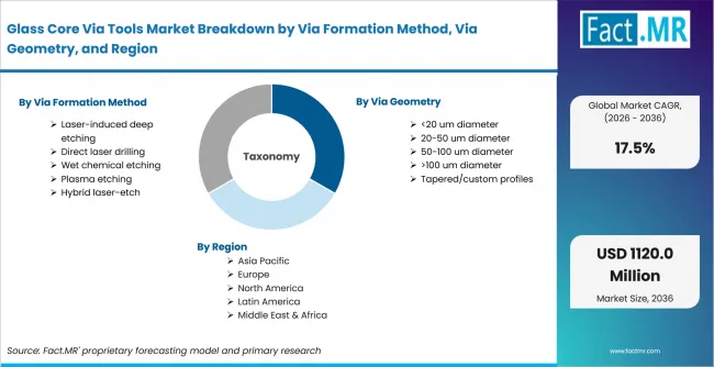
Glass Core Via Tools Market Breakdown By Via Formation Method, Via Geometry, And Region | Source: Fact.MR
| Attribute | Details |
|---|---|
| Quantitative Units | USD 224.0 million in 2026 to USD 1,120.0 million by 2036 at a 17.5% CAGR |
| Market Definition | Glass core via tools are the laser and etch systems that form through-glass vias (TGVs) in glass core substrates for advanced packaging: UV/CO2/excimer/ultrashort-pulse laser drilling, and laser-induced deep etching (LIDE) platforms combining femtosecond/picosecond laser modification with selective wet etch. This is a distinct equipment category from PCB drilling - specs target <100 µm pitch, high aspect ratio, and zero microcracks on 100-500 µm glass at panel sizes (510×515 mm, 600×600 mm). |
| Via Formation Method | Laser-induced deep etching; Direct laser drilling; Wet chemical etching; Plasma etching; Hybrid laser-etch |
| Via Geometry | <20 um diameter; 20-50 um diameter; 50-100 um diameter; >100 um diameter; Tapered/custom profiles |
| Glass Thickness | <300 um; 300-500 um; 500-800 um; >800 um; Custom thickness |
| Application | Glass core substrates; Interposers; RF/photonics packages; MEMS packaging; Display integration |
| End User | Substrate manufacturers; OSAT providers; Foundries; IDMs; R&D institutes |
| Regions Covered | North America; Latin America; Europe; East Asia; South Asia & Oceania; Middle East & Africa |
| Countries Covered | Japan; South Korea; Taiwan; Austria; USA |
| Key Companies Profiled | LPKF Laser & Electronics; Corning; Applied Materials; Schott; Via Mechanics; Disco |
| Forecast Period | 2026 to 2036 |
| Approach | Hybrid top-down and bottom-up approach using demand indicators across Via Formation Method; Via Geometry; Glass Thickness; Application; End User; country-level growth; company participation and adoption trends |
Source: Fact.MR analysis. Updated Jul 23, 2026
How is the market segmented?
-
By Via Formation Method
- Laser-induced deep etching
- Direct laser drilling
- Wet chemical etching
- Plasma etching
- Hybrid laser-etch
-
By Via Geometry
- <20 um diameter
- 20-50 um diameter
- 50-100 um diameter
- >100 um diameter
- Tapered/custom profiles
-
By Glass Thickness
- <300 um
- 300-500 um
- 500-800 um
- >800 um
- Custom thickness
-
By Application
- Glass core substrates
- Interposers
- RF/photonics packages
- MEMS packaging
- Display integration
-
By End User
- Substrate manufacturers
- OSAT providers
- Foundries
- IDMs
- R&D institutes
-
By Region
- North America
- Latin America
- Europe
- South Asia & Oceania
- Middle East & Africa
Frequently Asked Questions
Which Via Formation Method leads the Glass Core Via Tools Market?
Which Via Geometry leads the Glass Core Via Tools Market?
Which Glass Thickness leads the Glass Core Via Tools Market?
Which Application leads the Glass Core Via Tools Market?
Which End User leads the Glass Core Via Tools Market?
What CAGR is projected for China in the Glass Core Via Tools Market?
What CAGR is projected for USA in the Glass Core Via Tools Market?
What CAGR is projected for Taiwan in the Glass Core Via Tools Market?
What CAGR is projected for South Korea in the Glass Core Via Tools Market?
What CAGR is projected for Japan in the Glass Core Via Tools Market?
What CAGR is projected for Austria in the Glass Core Via Tools Market?
What is the primary driver of the Glass Core Via Tools Market?
What is the main restraint in the Glass Core Via Tools Market?
Who worked on this report


Preview the report firsthand - request a free sample
Free SampleGet the brochure for pricing and purchase details
Download PDF