- Market Value (2025): USD 506.2 Mn
- Estimated Value (2026): USD 572.0 Mn
- Forecast Value (2036): USD 1950.0 Mn
- CAGR (2026-2036): 13%
What is the High-Aspect Cryoetch Market forecast to be worth by 2036?
USD 572.0 million in 2026 to USD 1,950.0 million by 2036, at a 13.0% CAGR.
- The High-Aspect Cryoetch Market crossed a valuation of USD 506.2 million in 2025, supported by demand from Memory manufacturers serving Memory channel holes workflows that require controlling aspect-ratio-dependent etch, sidewall passivation and bottom transport in very deep features.
- Demand is projected to increase from USD 572.0 million in 2026 to USD 1,950.0 million by 2036.
- The market is forecast to record a 13.0% CAGR from 2026 to 2036 as the ARDE problem it solves, cooling hardware and quantified frontier remain central purchase reasons.
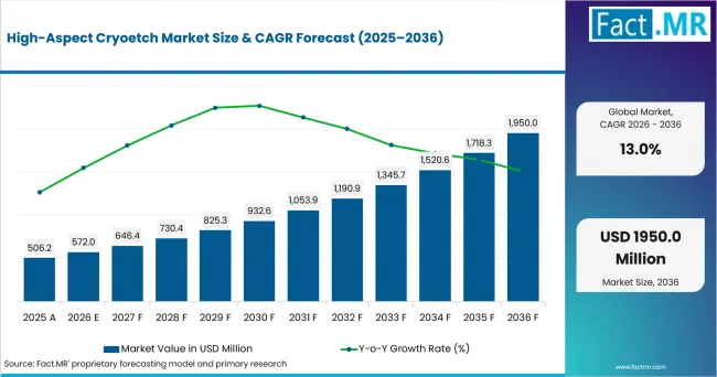
High Aspect Cryoetch Market Value Analysis | Source: Fact.MR
What are the defining numbers behind High-Aspect Cryoetch Market growth?
USD 1,378.0 million absolute opportunity is expected by 2036.
- Demand Drivers in the Market
- The ARDE problem it solves: Demand for cryogenic HAR etch tools is driven directly by aspect-ratio-dependent etching: in conventional RIE, etch rate drops as the hole deepens because ion flux and neutral transport starve the feature bottom, while cryogenics changes the adsorption regime, exploiting the temperature-dependent shift from chemisorption to physisorption of neutral species on the sidewalls to hold the profile, per Lam's Kim.
- Cooling hardware: Equipment demand is tied to a specific hardware architecture: ultra-low wafer temperature delivered through platform chillers plus helium backside wafer cooling, paired with scalable high-power confined plasma reactors for deep, narrow features and pulsed plasma technology that modulates species for profile and selectivity control.
- Quantified frontier: The throughput case for cryo HAR etch is now quantified: greater-than-400-layer 3D NAND needs at least 8 micrometers per tier of channel-hole depth to sustain two-tier stacks, and TEL's cryo process demonstrated 10 micrometer depth in 33 minutes versus an hours-class legacy process - the step-change in throughput that made cryo HAR production-worthy, with polymer buildup at the hole top the named failure mode limiting further gains.
- Chemistry innovation: Chemistry innovation is compounding the throughput gains: HF-based etching with trace PF3 catalysis promotes the reaction between HF and SiO2, increasing etch rates at lower operating temperature while cutting global-warming potential by 84%, pairing a performance gain with a sustainability gain that strengthens the purchase case.
- Key Segments Analyzed
- By Feature Type: Memory channel holes are projected to hold 32.0% share in 2026, supported by a clear process advantage: Memory channel holes combine extreme depth, dense repetition and tight profile requirements, creating the clearest production case for cryogenic adsorption and passivation control. Their etch time also has a direct effect on NAND fab productivity.
- By Aspect Ratio Class: 40-60:1 is projected to hold 40.8% share in 2026, supported by a clear process advantage: The 40-60:1 class is demanding enough to benefit materially from cryogenic chemistry while retaining a broader manufacturable window than the most extreme structures. It forms the bridge between conventional deep RIE and next-generation ultra-high-aspect etch.
- By Process Control: Profile/bow control is projected to hold 47.1% share in 2026, supported by a clear process advantage: Profile and bow control determine whether the bottom of a deep feature lands in the correct location and whether adjacent holes remain isolated. A fast etch has little value if sidewalls curve or twist with depth.
- By Substrate: Silicon is projected to hold 45.2% share in 2026, supported by a clear process advantage: Silicon provides the broadest base for deep trenches, TSVs and MEMS structures and has a mature cryogenic etch knowledge base. It therefore supports the widest equipment utilization beyond a single memory stack.
- By End User: Memory manufacturers are projected to hold 30.6% share in 2026, supported by a clear process advantage: Memory manufacturers run the highest-volume, most repetitive high-aspect features and can justify dedicated chamber fleets and recipe development. Their layer-count road maps continuously raise the depth and productivity requirement.
- Analyst Opinion at Fact.MR
- Shambhu Nath Jha, Sr. Consultant at Fact.MR, states, 'Buyers should evaluate the complete process sequence around controlling aspect-ratio-dependent etch, sidewall passivation and bottom transport in very deep features. Technical review should focus on repeatability, integration, defect control and production throughput rather than a single headline specification. Suppliers that connect tool performance to measurable yield and qualification results are likely to build trust faster.'
- Strategic Implications
- The tool must prove depth uniformity, bow control, selectivity and repeatability across the target feature family.
- Equipment suppliers should document how their systems address the challenge of controlling aspect-ratio-dependent etch, sidewall passivation and bottom transport in very deep features across production-representative wafers, panels, dies or packages.
- Procurement teams should assess anisotropy at high aspect ratios, sidewall roughness, profile control, cryogenic gas delivery, chamber stability and post-etch clean compatibility.
South Korea is projected to record a 13.9% CAGR as high-volume memory, HBM and vertically integrated semiconductor manufacturing supports relevant capital spending; Taiwan is projected to record a 14.2% CAGR as leading foundry production, advanced packaging and a dense OSAT and substrate supply chain supports relevant capital spending; USA is projected to record a 14.5% CAGR as leading-edge logic, high-performance computing, federally supported semiconductor R&D and a large domestic equipment base supports relevant capital spending; Japan is projected to record a 13.7% CAGR as semiconductor equipment, materials, inspection and memory-process expertise supports relevant capital spending; while Singapore is projected to record a 13.2% CAGR as advanced-packaging R&D, specialty fabs and regional assembly and test operations supports relevant capital spending through 2036.
How does the High-Aspect Cryoetch Market break down by segment?
Memory channel holes leads Feature Type with a 32.0% share, while 40-60:1 accounts for 40.8% of Aspect Ratio Class in 2026.
Why do Memory channel holes lead Feature Type?
Memory channel holes are projected to account for 32.0% share in 2026.
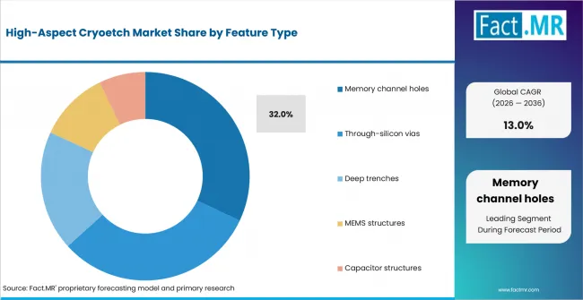
High Aspect Cryoetch Market Analysis By Feature Type | Source: Fact.MR
Memory channel holes combine extreme depth, dense repetition and tight profile requirements, creating the clearest production case for cryogenic adsorption and passivation control. Their etch time also has a direct effect on NAND fab productivity. TSVs are strategically important, but their volume and feature repetition are lower than channel holes in advanced memory. >400-Layer 3D NAND needs at least 8 µm/tier channel-hole depth to sustain 2-tier stacks (TEL's Kihara et al.); TEL's cryo process demonstrated 10 µm depth in 33 minutes (vs hours-class legacy) - the throughput step-change that made cryo HAR production-worthy. Polymer management at the hole top is the named failure mode: top polymers can stop the ion flux from reaching the feature bottom.
Why does 40-60:1 lead Aspect Ratio Class?
40-60:1 is projected to account for 40.8% share in 2026.
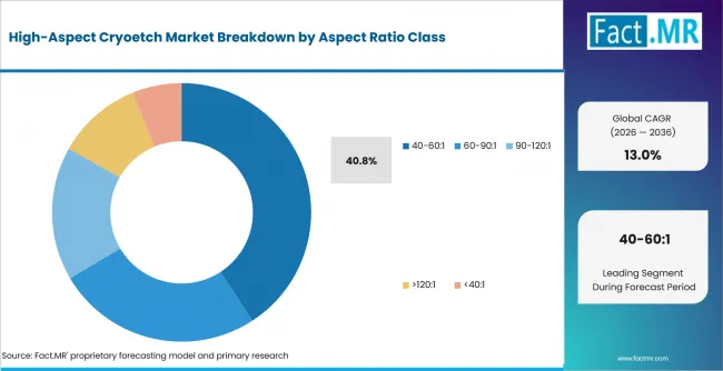
High Aspect Cryoetch Market Analysis By Aspect Ratio Class | Source: Fact.MR
The 40-60:1 class is demanding enough to benefit materially from cryogenic chemistry while retaining a broader manufacturable window than the most extreme structures. It forms the bridge between conventional deep RIE and next-generation ultra-high-aspect etch. The 60-90:1 class offers stronger technical differentiation but requires tighter temperature, transport and sidewall control. Aspect-ratio-dependent etching: in conventional RIE, etch rate drops as the hole deepens; ion flux and neutral transport starve the feature bottom. Cryogenics changes the adsorption regime: hole profile is controlled through the precise management of wafer temperature and gas chemistry, which exploits the temperature-dependent shift from chemisorption to physisorption of neutral species on the etch sidewalls (Lam's Kim). Buyers therefore tend to treat 40-60:1 as the practical choice when qualification must balance process capability, repeatability and production economics.
Why does Profile/bow control lead Process Control?
Profile/bow control is projected to account for 47.1% share in 2026.
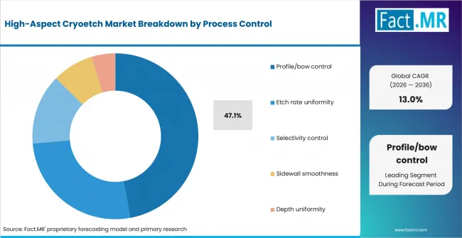
High Aspect Cryoetch Market Analysis By Process Control | Source: Fact.MR
Profile and bow control determine whether the bottom of a deep feature lands in the correct location and whether adjacent holes remain isolated. A fast etch has little value if sidewalls curve or twist with depth. Etch-rate uniformity is necessary, but profile error can create electrical failure even when nominal depth is on target. Near-perfect memory-hole profiles top-to-bottom - bowing, twisting, and CD uniformity across the wafer - are the purchase criteria; third generation of Lam's cryogenic technology, advanced etch chemistries and polymer management, combined with other etch innovations, offer better control of channel hole shape from top to bottom.
Why does Silicon lead Substrate?
Silicon is projected to account for 45.2% share in 2026.
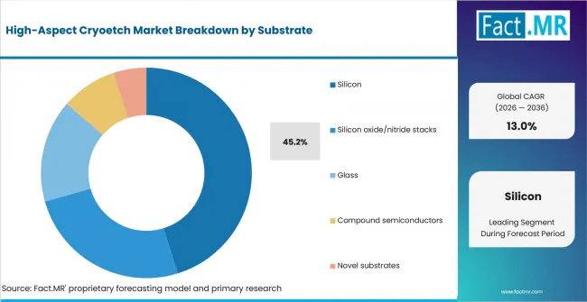
High Aspect Cryoetch Market Analysis By Substrate | Source: Fact.MR
Silicon provides the broadest base for deep trenches, TSVs and MEMS structures and has a mature cryogenic etch knowledge base. It therefore supports the widest equipment utilization beyond a single memory stack. Oxide-nitride stacks are central to 3D NAND but demand a more specialized dielectric chemistry and chamber configuration. Ultra-low wafer temperature via platform chillers + helium backside cooling of the wafer (Semiconductor Engineering). Reactor-side: scalable high-power confined plasma reactors generate the energetic plasma for deep, narrow features; unique pulsed plasma technology modulates species for profile and selectivity control. Buyers therefore tend to treat silicon as the practical choice when qualification must balance process capability, repeatability and production economics.
Why do Memory manufacturers lead End User?
Memory manufacturers are projected to account for 30.6% share in 2026.
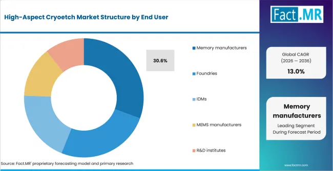
High Aspect Cryoetch Market Analysis By End User | Source: Fact.MR
Memory manufacturers run the highest-volume, most repetitive high-aspect features and can justify dedicated chamber fleets and recipe development. Their layer-count road maps continuously raise the depth and productivity requirement. Foundries use high-aspect etch across several devices, but the workload is more fragmented by application. HF-based etching with PF3 catalysis: small amounts of phosphorus-containing PF3 act as catalyst to promote the reaction between HF and SiO2, increasing etch rates at lower temperature operation, while cutting GWP 84% (TEL). Buyers therefore tend to treat memory manufacturers as the practical choice when qualification must balance process capability, repeatability and production economics.
What is accelerating High-Aspect Cryoetch Market adoption, and what is holding it back?
The strongest accelerator is the ARDE problem it solves, while the main restraint is that different substrates and mask stacks need distinct adsorption and passivation conditions, limiting recipe portability.
Drivers Impact Analysis
| DRIVER | (~) % IMPACT ON CAGR | GEOGRAPHIC RELEVANCE | IMPACT TIMELINE |
|---|---|---|---|
| The ARDE problem it solves | +3.6% | Global leading-edge fabs | Medium term (2-4 years) |
| Cooling hardware | +3.0% | Global leading-edge fabs | Medium term (2-4 years) |
| Quantified frontier | +2.5% | Global leading-edge fabs | Short term (<=2 years) |
| Chemistry innovation | +1.9% | Global leading-edge fabs | Medium term (2-4 years) |
Source: Fact.MR analysis. Updated Jul 23, 2026
- The ARDE problem it solves: Aspect-ratio-dependent etching: in conventional RIE, etch rate drops as the hole deepens; ion flux and neutral transport starve the feature bottom. Cryogenics changes the adsorption regime: hole profile is controlled through the precise management of wafer temperature and gas chemistry, which exploits the temperature-dependent shift from chemisorption to physisorption of neutral species on the etch sidewalls (Lam's Kim).
- Cooling hardware: Ultra-low wafer temperature via platform chillers + helium backside cooling of the wafer (Semiconductor Engineering). Reactor-side: scalable high-power confined plasma reactors generate the energetic plasma for deep, narrow features; unique pulsed plasma technology modulates species for profile and selectivity control.
- Quantified frontier: >400-Layer 3D NAND needs at least 8 µm/tier channel-hole depth to sustain 2-tier stacks (TEL's Kihara et al.); TEL's cryo process demonstrated 10 µm depth in 33 minutes (vs hours-class legacy) - the throughput step-change that made cryo HAR production-worthy. Polymer management at the hole top is the named failure mode: top polymers can stop the ion flux from reaching the feature bottom.
- Chemistry innovation: HF-based etching with PF3 catalysis: small amounts of phosphorus-containing PF3 act as catalyst to promote the reaction between HF and SiO2, increasing etch rates at lower temperature operation, while cutting GWP 84% (TEL).
Opportunity Impact Analysis
| OPPORTUNITY | (~) % IMPACT ON CAGR | GEOGRAPHIC RELEVANCE | IMPACT TIMELINE |
|---|---|---|---|
| Multi-tier vs single-etch-deep fork | +2.2% | Global leading-edge fabs | Medium term (2-4 years) |
| Pulsed plasma control | +1.7% | Global leading-edge fabs | Medium term (2-4 years) |
| Environmental co-design | +1.3% | Global leading-edge fabs | Short term (<=2 years) |
Source: Fact.MR analysis. Updated Jul 23, 2026
- Multi-tier vs single-etch-deep fork: Deeper single-etch (fewer tiers, fewer stitch interfaces) vs more tiers (easier etch, more litho/alignment) - the etcher's achievable depth sets the economic optimum; at least 8 µm/tier currently anchors 2-tier designs.
- Pulsed plasma control: Time-multiplexed source/bias pulsing tunes ion energy and neutral flux to suppress ARDE and bowing at the deepest features (Lam technology pillars).
Restraints Impact Analysis
| RESTRAINT | (~) % IMPACT ON CAGR | GEOGRAPHIC RELEVANCE | IMPACT TIMELINE |
|---|---|---|---|
| Primary qualification constraint | -1.9% | Global leading-edge fabs | Medium term (2-4 years) |
| Process-window sensitivity | -1.6% | Global leading-edge fabs | Medium term (2-4 years) |
| Thermal and mechanical distortion | -1.2% | Global leading-edge fabs | Medium term (2-4 years) |
Source: Fact.MR analysis. Updated Jul 23, 2026
- Primary qualification constraint: Different substrates and mask stacks need distinct adsorption and passivation conditions, limiting recipe portability.
- Process-window sensitivity: Polymer management at the hole top is the named failure mode: top polymers can stop the ion flux from reaching the feature bottom.
- Thermal and mechanical distortion: Near-perfect memory-hole profiles top-to-bottom - bowing, twisting, and CD uniformity across the wafer - are the purchase criteria; third generation of Lam's cryogenic technology, advanced etch chemistries and polymer management, combined with other etch innovations, offer better control of channel hole shape from top to bottom.
Which countries are scaling High-Aspect Cryoetch Market fastest?
In USA, High Aspect Cryoetch Market is projected to advance at 14.5% CAGR, supported by leading-edge logic, high-performance computing, federally supported semiconductor R&D and a large domestic equipment base.
- Countries differ less by the headline CAGR than by the type of semiconductor work creating demand for the High-Aspect Cryoetch Market.
- USA follows a pathway shaped by leading-edge logic, high-performance computing, federally supported semiconductor R&D and a large domestic equipment base. China takes a different path through rapid domestic capacity build-out, local-equipment substitution and tighter access to controlled foreign tools.
- Taiwan demand is tied to foundry and memory-layer process development, whereas South Korea demand is tied to high-volume memory investment and domestic equipment integration.
- Japan contributes cryogenic-etch equipment, materials and process-development capability, while Singapore supports packaging R&D, specialty fabrication and regional assembly operations.
- Demand differs with 3D NAND and memory investment, high-aspect-ratio process requirements, local etch-tool availability and qualification cycles.
The country review considers six profiled markets alongside the wider coverage of North America, Latin America, Europe, East Asia, South Asia & Oceania, and the Middle East & Africa.
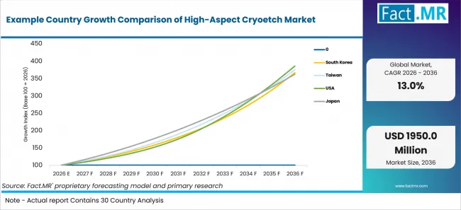
Example Country Growth Comparison Of High Aspect Cryoetch Market | Source: Fact.MR
| COUNTRY | CAGR, 2026 to 2036 |
|---|---|
| USA | 14.5% |
| Taiwan | 14.2% |
| South Korea | 13.9% |
| Japan | 13.7% |
| Singapore | 13.2% |
Source: Fact.MR analysis. Updated Jul 23, 2026
What is driving USA's growth through 2036?
14.5% CAGR, supported by leading-edge logic, high-performance computing, federally supported semiconductor R&D and a large domestic equipment base.
Lam - cryo HAR franchise (Flex/Vantex + Cryo 3.0); Micron ramping high-layer NAND domestically. This environment creates a clear qualification pathway for the High-Aspect Cryoetch Market because buyers must solve the problem of controlling aspect-ratio-dependent etch, sidewall passivation and bottom transport in very deep features at production scale.
What is driving Taiwan's growth through 2036?
14.2% CAGR, supported by leading foundry production, advanced packaging and a dense OSAT and substrate supply chain.
TSMC-led foundry scale, advanced packaging capacity and a dense OSAT and substrate network support Taiwan’s CAGR through 2036. This environment creates a clear qualification pathway for the market because semiconductor manufacturers must improve process control, yield and throughput across leading-edge wafer fabrication and high-density packaging at production scale.
What is driving South Korea's growth through 2036?
13.9% CAGR, supported by high-volume memory, HBM and vertically integrated semiconductor manufacturing.
Samsung/SK hynix - largest HAR etch installed base; multi-tier strategies differ (Samsung 2-tier focus, others evaluate 3-tier). This environment creates a clear qualification pathway for the High-Aspect Cryoetch Market because buyers must solve the problem of controlling aspect-ratio-dependent etch, sidewall passivation and bottom transport in very deep features at production scale.
What is driving Japan's growth through 2036?
13.7% CAGR, reflecting Japan's cryogenic-etch development base and supplier expertise across equipment, materials and process control.
TEL - cryo breakthrough from Miyagi; Kioxia home demand. This environment creates a clear qualification pathway for the High-Aspect Cryoetch Market because buyers must solve the problem of controlling aspect-ratio-dependent etch, sidewall passivation and bottom transport in very deep features at production scale.
What is driving Singapore's growth through 2036?
13.2% CAGR, supported by advanced-packaging R&D, specialty fabs and regional assembly and test operations.
Singapore combines advanced-packaging R&D, specialty fabs and regional assembly and test operations with a 6.8% share of 2026 demand across the six profiled countries. Aspect-ratio-dependent etching: in conventional RIE, etch rate drops as the hole deepens; ion flux and neutral transport starve the feature bottom. The commercial link is the need to solve the problem of controlling aspect-ratio-dependent etch, sidewall passivation and bottom transport in very deep features as capacity and process complexity increase.
Who leads the High-Aspect Cryoetch Market?
Lam Research and Tokyo Electron lead the competitive landscape, followed by Applied Materials and Oxford Instruments as the next tier of challengers.
Lam Research participates through etch, deposition, clean and advanced memory process integration, with relevance determined by its ability to address the challenge of controlling aspect-ratio-dependent etch, sidewall passivation and bottom transport in very deep features. Tokyo Electron participates through etch, clean, deposition and wafer-bonding process equipment. 10 Μm/33 min cryo channel-hole process; HF/PF3 chemistry; −84% GWP. Applied Materials participates through deposition, etch, materials engineering and integrated process modules, with relevance determined by its ability to address the challenge of controlling aspect-ratio-dependent etch, sidewall passivation and bottom transport in very deep features. Oxford Instruments participates through plasma etch, deposition and materials processing, with relevance determined by its ability to address the challenge of controlling aspect-ratio-dependent etch, sidewall passivation and bottom transport in very deep features.
SPTS (KLA) holds a more specialized role through specialized semiconductor equipment, particularly where custom integration and service coverage affect qualification. Hitachi High-Tech holds a more specialized role through CD-SEM and semiconductor inspection, particularly where custom integration and service coverage affect qualification.
Competition is expected to center on repeatable process performance, integration with adjacent modules, installed-base service and documented capability to address the challenge of controlling aspect-ratio-dependent etch, sidewall passivation and bottom transport in very deep features. Buyers are likely to compare accuracy, defect prevention, throughput, recipe stability and the completeness of the delivered process cell.
Which companies are the key providers?
Key companies include Lam Research; Tokyo Electron; Applied Materials; Oxford Instruments; SPTS (KLA); Hitachi High-Tech.
- Lam Research
- Tokyo Electron
- Applied Materials
- Oxford Instruments
- SPTS (KLA)
- Hitachi High-Tech
Bibliography
- Tokyo Electron Limited. (2023, June 9). Tokyo Electron develops memory channel hole etch technology that enables ultra-fast 10-μm-deep etching for 3D NAND flash with over 400 layers and an 84% reduction of global warming potential.
- Kihara, Y., Tomura, M., Sakamoto, W., Honda, M., & Kojima, M. (2023). Beyond 10 μm depth ultra-high speed etch process with 84% lower carbon footprint for memory channel hole of 3D NAND flash over 400 layers. In 2023 Symposium on VLSI Technology and Circuits. IEEE.
- Lam Research Corporation. (2024, July 31). Lam Research introduces Lam Cryo™ 3.0 cryogenic etch technology to accelerate scaling of 3D NAND for the AI era.
- Singh, H. (2024, July 31). Lam Cryo 3.0: What you need to know. Lam Research Corporation.
This Report Addresses
- The report provides strategic intelligence on High-Aspect Cryoetch Market across Feature Type and Aspect Ratio Class choices that shape purchasing decisions.
- Segment analysis covers Memory channel holes as the share leader within the 2026 market structure.
- Regional outlook evaluates South Korea and Taiwan alongside USA and Japan, while Singapore complete the growth comparison.
- Competitive analysis profiles Lam Research and Tokyo Electron alongside Applied Materials and Oxford Instruments, followed by additional active providers.
- Use-case assessment covers the categories and applications that shape demand in the High-Aspect Cryoetch Market across the forecast period.
What does the High-Aspect Cryoetch Market cover?
The market covers equipment and process systems configured to address the challenge of controlling aspect-ratio-dependent etch, sidewall passivation and bottom transport in very deep features.
High-aspect cryoetch is the physics-defined equipment segment for etching features with extreme depth-to-width ratios (typically >40:1, heading beyond 100:1) at cryogenic wafer temperatures - 3D NAND channel holes and staircases today, with DRAM capacitor and advanced logic HAR structures adjacent. It is distinct from the NAND-specific market view: this file covers the enabling physics, reactor engineering, and cross-device applicability of cryogenic HAR etching.
Commercial value includes cryogenic etch chambers, RF power delivery, low-temperature control, gas handling, wafer transport, endpoint control and service integration. Finished devices, package value and unrelated lithography or deposition equipment are excluded.
What is included in the scope?
The scope includes systems used by memory manufacturers and the other end-user groups listed in the segmentation.
The market is segmented by Feature Type, including Memory channel holes, Through-silicon vias, Deep trenches, MEMS structures, Capacitor structures; Aspect Ratio Class, including 40-60:1, 60-90:1, 90-120:1, >120:1, <40:1; Process Control, including Profile/bow control, Etch rate uniformity, Selectivity control, Sidewall smoothness, Depth uniformity; Substrate, including Silicon, Silicon oxide/nitride stacks, Glass, Compound semiconductors, Novel substrates; End User, including Memory manufacturers, Foundries, IDMs, MEMS manufacturers, R&D institutes.
Cryogenic gas delivery, temperature-control, wafer handling, endpoint, clean and chamber-control modules are included only when delivered with the configured etch platform.
What is excluded from the scope?
The scope excludes unrelated semiconductor equipment, standalone materials and components sold independently of the configured system.
It also excludes facility construction, cleanroom infrastructure, the value of processed wafers or packages, and adjacent process steps that are not part of the defined equipment category.
How Was the Analysis Built?
Fact.MR is of the opinion that this assessment combines structured market analysis with a review of public information and industry evidence relevant to the market.
- Market Assessment: The analysis considers demand patterns, supply conditions, segment mix, country activity, company participation, and adoption trends.
- Evidence Review: Public company disclosures, government and regulatory publications, trade information, technical literature, and industry records inform the assessment.
- Validation and Updates: Findings are cross-checked against available market indicators and reviewed when material market developments emerge.
Segmentation
What is the report's scope and coverage?
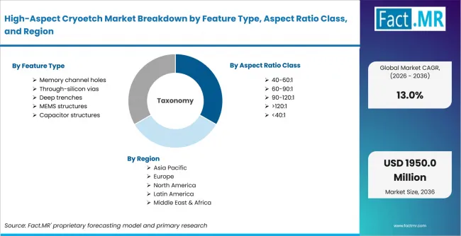
High Aspect Cryoetch Market Breakdown By Feature Type, Aspect Ratio Class, And Region | Source: Fact.MR
| Attribute | Details |
|---|---|
| Quantitative Units | USD 572.0 million in 2026 to USD 1,950.0 million by 2036 at a 13.0% CAGR |
| Market Definition | High-aspect cryoetch is the physics-defined equipment segment for etching features with extreme depth-to-width ratios (typically >40:1, heading beyond 100:1) at cryogenic wafer temperatures - 3D NAND channel holes and staircases today, with DRAM capacitor and advanced logic HAR structures adjacent. It is distinct from the NAND-specific market view: this file covers the enabling physics, reactor engineering, and cross-device applicability of cryogenic HAR etching. |
| Feature Type | Memory channel holes; Through-silicon vias; Deep trenches; MEMS structures; Capacitor structures |
| Aspect Ratio Class | 40-60:1; 60-90:1; 90-120:1; >120:1; <40:1 |
| Process Control | Profile/bow control; Etch rate uniformity; Selectivity control; Sidewall smoothness; Depth uniformity |
| Substrate | Silicon; Silicon oxide/nitride stacks; Glass; Compound semiconductors; Novel substrates |
| End User | Memory manufacturers; Foundries; IDMs; MEMS manufacturers; R&D institutes |
| Regions Covered | North America; Latin America; Europe; East Asia; South Asia & Oceania; Middle East & Africa |
| Countries Covered | South Korea; Taiwan; USA; Japan; Singapore |
| Key Companies Profiled | Lam Research; Tokyo Electron; Applied Materials; Oxford Instruments; SPTS (KLA); Hitachi High-Tech |
| Forecast Period | 2026 to 2036 |
| Approach | Hybrid top-down and bottom-up approach using demand indicators across Feature Type; Aspect Ratio Class; Process Control; Substrate; End User; country-level growth; company participation and adoption trends |
Source: Fact.MR analysis. Updated Jul 23, 2026
How is the market segmented?
-
By Feature Type
- Memory channel holes
- Through-silicon vias
- Deep trenches
- MEMS structures
- Capacitor structures
-
By Aspect Ratio Class
- 40-60:1
- 60-90:1
- 90-120:1
- >120:1
- <40:1
-
By Process Control
- Profile/bow control
- Etch rate uniformity
- Selectivity control
- Sidewall smoothness
- Depth uniformity
-
By Substrate
- Silicon
- Silicon oxide/nitride stacks
- Glass
- Compound semiconductors
- Novel substrates
-
By End User
- Memory manufacturers
- Foundries
- IDMs
- MEMS manufacturers
- R&D institutes
-
By Region
- North America
- USA
- Latin America
- Other regional markets assessed at aggregate level
- Europe
- Other regional markets assessed at aggregate level
- East Asia
- South Korea
- Taiwan
- Taiwan
- Japan
- China
- South Asia & Oceania
- Singapore
- Middle East & Africa
- Other regional markets assessed at aggregate level
- North America
Frequently Asked Questions
Which Feature Type leads the High-Aspect Cryoetch Market?
Which Aspect Ratio Class leads the High-Aspect Cryoetch Market?
Which Process Control leads the High-Aspect Cryoetch Market?
Which Substrate leads the High-Aspect Cryoetch Market?
Which End User leads the High-Aspect Cryoetch Market?
What CAGR is projected for USA in the High-Aspect Cryoetch Market?
What CAGR is projected for Taiwan in the High-Aspect Cryoetch Market?
What CAGR is projected for South Korea in the High-Aspect Cryoetch Market?
What CAGR is projected for Japan in the High-Aspect Cryoetch Market?
What CAGR is projected for Singapore in the High-Aspect Cryoetch Market?
What is the primary driver of the High-Aspect Cryoetch Market?
What is the main restraint in the High-Aspect Cryoetch Market?
Who worked on this report


Preview the report firsthand - request a free sample
Free SampleGet the brochure for pricing and purchase details
Download PDF