- Market Value (2025): USD 352.0 Mn
- Estimated Value (2026): from USD 402.0 Mn
- Forecast Value (2036): USD 1520.0 Mn
- CAGR (2026-2036):14.2%
What is the Copper Hybrid Interfaces Market forecast to be worth by 2036?
USD 402.0 million in 2026 to USD 1,520.0 million by 2036, at a 14.2% CAGR.
- The Copper Hybrid Interfaces Market crossed a valuation of USD 352.0 million in 2025, supported by demand from Memory manufacturers serving Cu bond pads workflows that require forming low-resistance copper-to-copper connections while preserving dielectric bond integrity, copper recess and oxide-free surfaces.
- Demand is projected to increase from USD 402.0 million in 2026 to USD 1,520.0 million by 2036.
- The market is forecast to record a 14.2% CAGR from 2026 to 2036 as two-phase bond formation, dishing spec and recess failure mode remain central purchase reasons.
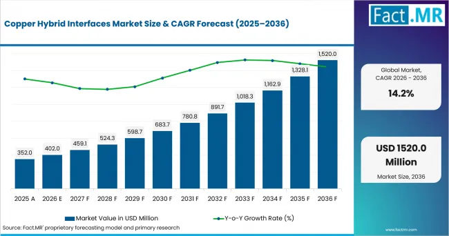
Copper Hybrid Interfaces Market Value Analysis | Source: Fact.MR
What are the defining numbers behind Copper Hybrid Interfaces Market growth?
USD 1,118.0 million absolute opportunity is expected by 2036.
- Demand Drivers in the Market
- Two-phase bond formation: Demand for tightly sequenced anneal equipment stems from the two-phase physics of the bond itself: room-temperature dielectric bonding - van der Waals plus covalent Si-O-Si bonds after activation - holds the stack together, and only during a 150-400 degrees C anneal do the recessed copper pads expand by CTE mismatch, close the recess gap, and fuse by grain-boundary and surface diffusion into a dense joint. [1][2]
- Dishing spec: CMP tool specifications are tightening around a hard dishing target: BESI typically targets 5 nm dishing or below, since CMP must avoid dielectric erosion that would expose the barrier layer around the pad and prevent bonding, per BESI's Abdilla via Semiconductor Engineering.
- Recess failure mode: A well-documented failure mode is pushing buyers toward tighter recess control: once copper recess exceeds a few nanometers, bonding force transfers onto the surrounding oxide, weakening the Cu-Cu interface and causing incomplete or unreliable bonds, an effect compounded in chiplet-to-wafer flows by chiplet-to-chiplet pad-height variation. [3]
- Oxidation is the central metallurgical risk: Copper oxidation is emerging as the central metallurgical risk shaping equipment choice: TEM/EELS analysis on FIB lamella shows a thin copper-oxide interfacial layer at the Cu-Cu plane that shows up electrically as elevated contact resistance or an open circuit even with intact dielectric bonding, and NYCU researchers confirm the thermal budget needed to drive copper diffusion also risks warpage and BEOL degradation. [4][1]
- Key Segments Analyzed
- By Interface Layer: Cu bond pads are projected to hold 33.0% share in 2026, supported by a clear process advantage: Copper bond pads carry the electrical connection across the hybrid interface, so their recess, oxide state and local planarity directly determine contact resistance. A mechanically bonded stack can therefore pass visual inspection while still containing electrically open copper contacts.
- By Deposition Method: PVD deposition is projected to hold 48.3% share in 2026, supported by a clear process advantage: PVD is widely used to form adhesion, barrier and seed layers with tight thickness control before copper plating or pad formation. This makes PVD integration and chamber-to-chamber control important when suppliers qualify repeatable barrier and seed-layer stacks.
- By Pad Pitch: <1 um is projected to hold 41.0% share in 2026, supported by a clear process advantage: Below 1 micrometer, hybrid bonding replaces solder bumps with direct copper contacts and unlocks a step change in interconnect density. The same scaling makes recess, oxidation and overlay errors proportionally more damaging.
- By Application: HBM/DRAM stacks are projected to hold 40.6% share in 2026, supported by a clear process advantage: HBM and DRAM stacks require thousands of short, low-resistance vertical paths and benefit directly from the pitch and electrical performance of copper hybrid interfaces. Repeated layers also magnify any contact-resistance distribution or open defect.
- By End User: Memory manufacturers are projected to hold 33.0% share in 2026, supported by a clear process advantage: Memory manufacturers qualify copper interfaces as part of the complete HBM stack, linking CMP, cleaning, bonding and anneal to final electrical yield. Their high-volume repetition supports dedicated process modules and statistical control.
- Analyst Opinion at Fact.MR
- Shambu Nath Jha, Sr. Consultant at Fact.MR, states, 'Buyers should evaluate the complete copper-to-copper interface rather than treating bond alignment as the only qualification metric. Process review should combine CMP control, surface activation, oxide management, alignment, anneal and electrical-yield evidence on production-representative wafers. Suppliers that document interface resistance, open-defect rates, overlay stability and integration requirements will give engineering and procurement teams a stronger basis for selection.'
- Strategic Implications
- Process ownership must span CMP, activation, cleaning, bond alignment and anneal because electrical opens often originate upstream of the bond chamber.
- Equipment suppliers should document how their systems address the challenge of forming low-resistance copper-to-copper connections while preserving dielectric bond integrity, copper recess and oxide-free surfaces across production-representative wafers, panels, dies or packages.
- Procurement teams should compare CMP and surface-preparation requirements, bond alignment, oxide control, anneal conditions, electrical-yield evidence and service support before selecting a hybrid-bonding platform.
South Korea is projected to record a 15.7% CAGR as high-volume memory, HBM and vertically integrated semiconductor manufacturing supports relevant capital spending; Taiwan is projected to record a 15.5% CAGR as leading foundry production, advanced packaging and a dense OSAT and substrate supply chain supports relevant capital spending; USA is projected to record a 15.7% CAGR as leading-edge logic, high-performance computing, federally supported semiconductor R&D and a large domestic equipment base supports relevant capital spending; Japan is projected to record a 14.9% CAGR as semiconductor equipment, materials, inspection and memory-process expertise supports relevant capital spending; while Singapore is projected to record a 14.4% CAGR as advanced-packaging R&D, specialty fabs and regional assembly and test operations supports relevant capital spending through 2036.
How does the Copper Hybrid Interfaces Market break down by segment?
Cu bond pads leads Interface Layer with a 33.0% share, while PVD deposition accounts for 48.3% of Deposition Method in 2026.
Why do Cu bond pads lead Interface Layer?
Cu bond pads are projected to account for 33.0% share in 2026.
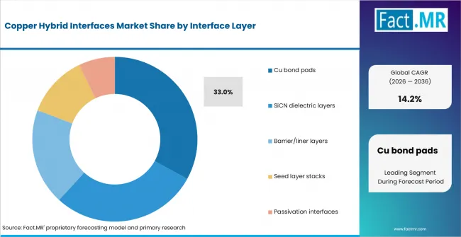
Copper Hybrid Interfaces Market Analysis By Interface Layer | Source: Fact.MR
Copper bond pads carry the electrical connection across the hybrid interface, so their recess, oxide state and local planarity directly determine contact resistance. The dielectric bond can hold the wafers together even when a copper contact remains electrically open. SiCN and other dielectric layers are essential to mechanical bonding, but copper pads are the element that converts the interface into a dense electrical interconnect. TEM/EELS on FIB lamella shows a Cu-oxide interface as a thin interfacial layer at the Cu-Cu plane; electrical signature is elevated contact resistance or open with intact dielectric bonding (failure-analysis reference). NYCU researchers confirmed Cu oxidation is a central challenge because the thermal budget driving Cu diffusion risks warpage and BEOL degradation. [4][1] Copper bond pads remain central because recess, oxide condition and local planarity directly govern whether the interface forms a low-resistance electrical connection.
Why does PVD deposition lead Deposition Method?
PVD deposition is projected to account for 48.3% share in 2026.
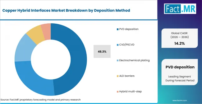
Copper Hybrid Interfaces Market Analysis By Deposition Method | Source: Fact.MR
PVD is widely used to form adhesion, barrier and seed layers with tight thickness control before copper plating or pad formation. Its installed base and integration with vacuum process modules support repeatable interface stacks. CVD and PECVD provide superior conformality for some films, but the dominant copper-pad flow still relies heavily on PVD-defined seed and barrier layers. Barrier exposure can prevent bonding, so PVD-defined seed and barrier layers must be controlled together with CMP and surface preparation. [2]
Why does <1 um lead Pad Pitch?
<1 um is projected to account for 41.0% share in 2026.
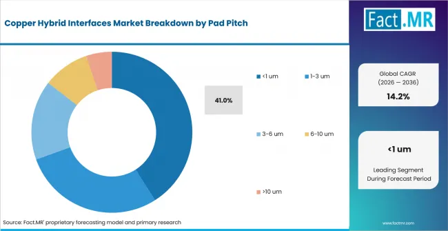
Copper Hybrid Interfaces Market Analysis By Pad Pitch | Source: Fact.MR
Below 1 micrometer, hybrid bonding replaces solder bumps with direct copper contacts and unlocks a step change in interconnect density. The same scaling makes recess, oxidation and overlay errors proportionally more damaging. The 1-3 micrometer range is easier to manufacture and inspect, but it offers less routing density for the most aggressive memory and logic stacks. Roadmaps (imec, CEA-Leti, Sony heritage in CIS) push Cu pad pitch from ~10 µm toward 1 µm and below, driving barrier-less Cu processes and interface-aware anneal profiles. Sub-1 µm pitches raise the value of overlay control, surface preparation and defect inspection because small recess or oxidation errors affect a larger share of each contact.
Why do HBM/DRAM stacks lead Application?
HBM/DRAM stacks are projected to account for 40.6% share in 2026.
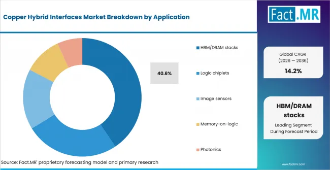
Copper Hybrid Interfaces Market Analysis By Application | Source: Fact.MR
HBM and DRAM stacks require dense, low-resistance vertical interconnects across repeated memory layers. Hybrid bonding supports finer pitch than solder-bump approaches, but it also increases the need for consistent copper recess, surface preparation, alignment and electrical-yield control throughout the stack.
Why do Memory manufacturers lead End User?
Memory manufacturers are projected to account for 33.0% share in 2026.
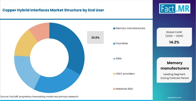
Copper Hybrid Interfaces Market Analysis By End User | Source: Fact.MR
Memory manufacturers qualify copper interfaces as part of the complete HBM stack, linking CMP, cleaning, bonding and anneal to final electrical yield. Their high-volume repetition supports dedicated process modules and statistical control. Foundries require broader design flexibility, whereas memory producers can optimize around standardized vertical interconnect arrays. Memory manufacturers favor hybrid-bonding flows that can repeat the same interface geometry across high-volume HBM and DRAM stacks while linking upstream process control to final electrical yield.
What is accelerating Copper Hybrid Interfaces Market adoption, and what is holding it back?
The strongest accelerator is two-phase bond formation, while the main restraint is that nanometer-scale dishing, oxide growth or trapped contamination can produce high resistance even when gross alignment appears acceptable.
Drivers Impact Analysis
| DRIVER | (~) % IMPACT ON CAGR | GEOGRAPHIC RELEVANCE | IMPACT TIMELINE |
|---|---|---|---|
| Two-phase bond formation | +4.0% | Global leading-edge fabs | Medium term (2-4 years) |
| Dishing spec | +3.3% | Global leading-edge fabs | Medium term (2-4 years) |
| Recess failure mode | +2.7% | Global leading-edge fabs | Short term (<=2 years) |
| Oxidation is the central metallurgical risk | +2.1% | Global leading-edge fabs | Medium term (2-4 years) |
Source: Fact.MR analysis. Updated Jul 22, 2026
- Two-phase bond formation: Room-temperature dielectric bonding (van der Waals + covalent Si-O-Si after activation) holds the stack; during 150-400 °C anneal the recessed Cu pads expand by CTE mismatch, close the recess gap, and fuse by grain-boundary and surface diffusion into a dense joint (mechanism review, citing NYCU 2023 work on Cu oxidation risk). [1][2]
- Dishing specification: We typically look at 5 nm dishing or below, while CMP must avoid dielectric erosion that would expose the barrier layer around the pad and prevent bonding (Besi's Abdilla via Semiconductor Engineering).
- Recess failure mode: If Cu recess exceeds a few nm, bonding force transfers to surrounding oxide, weakening the Cu-Cu interface and causing incomplete/unreliable bonds; chiplet-to-chiplet pad-height variation compounds this in C2W (SMTA 2025, §7). [3]
- Oxidation is the central metallurgical risk: TEM/EELS on FIB lamella shows a Cu-oxide interface as a thin interfacial layer at the Cu-Cu plane; electrical signature is elevated contact resistance or open with intact dielectric bonding (failure-analysis reference). Copper oxidation raises contact resistance and can leave electrical opens even when the dielectric interface remains bonded. [1][4]
Opportunity Impact Analysis
| OPPORTUNITY | (~) % IMPACT ON CAGR | GEOGRAPHIC RELEVANCE | IMPACT TIMELINE |
|---|---|---|---|
| Pitch scaling below 1 µm | +2.4% | Global leading-edge fabs | Medium term (2-4 years) |
| Barrier/adhesion engineering | +1.8% | Global leading-edge fabs | Medium term (2-4 years) |
| Low-temperature anneal chemistry | +1.4% | Global leading-edge fabs | Medium term (2-4 years) |
Source: Fact.MR analysis. Updated Jul 22, 2026
- Pitch scaling below 1 µm: Roadmaps (imec, CEA-Leti, Sony heritage in CIS) push Cu pad pitch from ~10 µm toward 1 µm and below, driving barrier-less Cu processes and interface-aware anneal profiles.
- Barrier/adhesion engineering: Barrier exposure can prevent bonding, so seed and barrier layers must be controlled together with CMP, cleaning and surface preparation. [2]
- Low-temperature anneal chemistry: Water-vapor-plasma dielectric activation (Adeia patents) and protective-layer workflows (SMTA) both aim to cut the thermal budget that oxidizes Cu.
Restraints Impact Analysis
| RESTRAINT | (~) % IMPACT ON CAGR | GEOGRAPHIC RELEVANCE | IMPACT TIMELINE |
|---|---|---|---|
| Primary qualification constraint | -2.1% | Global leading-edge fabs | Medium term (2-4 years) |
| Surface-state degradation | -1.7% | Global leading-edge fabs | Medium term (2-4 years) |
| Buried-defect escape | -1.3% | Global leading-edge fabs | Medium term (2-4 years) |
Source: Fact.MR analysis. Updated Jul 22, 2026
- Primary qualification constraint: Nanometer-scale dishing, oxide growth or trapped contamination can produce high resistance even when gross alignment appears acceptable. [1][2]
- Surface-state degradation: Oxide regrowth, contamination and out-of-window copper recess can prevent the metal surfaces from closing during anneal, creating high-resistance or open contacts. [1][2][4]
- Buried-defect escape: Besi reports a typical target of 5 nm dishing or below, while CMP must avoid dielectric erosion that exposes the barrier layer and prevents bonding. [2]
Which countries are scaling Copper Hybrid Interfaces Market fastest?
Japan is projected to record a 14.9% CAGR in the Copper Hybrid Interfaces Market, supported by its semiconductor equipment, materials, inspection and memory-process expertise.
- Countries differ less by the headline CAGR than by the type of semiconductor work creating demand for the Copper Hybrid Interfaces Market.
- South Korea follows a pathway shaped by high-volume memory, HBM and vertically integrated semiconductor manufacturing. USA takes a different path through leading-edge logic, high-performance computing, federally supported semiconductor R&D and a large domestic equipment base.
- Taiwan remains aligned through its combination of device production, equipment development and advanced packaging investment.
- Japan develops through semiconductor equipment, materials, inspection and memory-process expertise, while Singapore relies on advanced-packaging R&D, specialty fabs and regional assembly and test operations.
- Comparable growth rates can reflect different adoption paths because each country has a different mix of memory, logic, foundry, OSAT, equipment and materials capabilities.
The full report compares the five named country markets within the wider regional coverage of North America, Latin America, Europe, East Asia, South Asia & Oceania, and the Middle East & Africa.
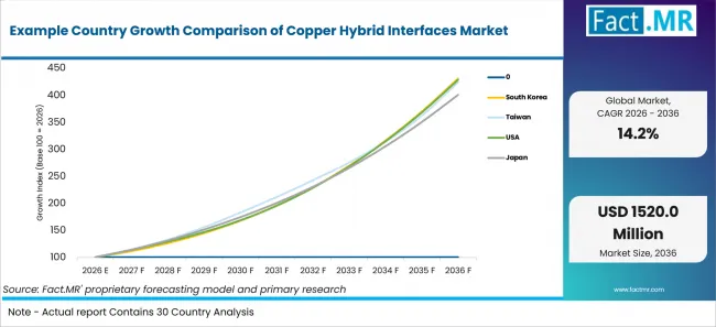
Example Country Growth Comparison Of Copper Hybrid Interfaces Market | Source: Fact.MR
| COUNTRY | CAGR, 2026 to 2036 |
|---|---|
| South Korea | 15.7% |
| USA | 15.7% |
| Taiwan | 15.5% |
| Japan | 14.9% |
| Singapore | 14.4% |
Source: Fact.MR analysis. Updated Jul 22, 2026
What is driving South Korea's growth through 2036?
15.7% CAGR, supported by high-volume memory, HBM and vertically integrated semiconductor manufacturing.
South Korea's memory and HBM manufacturing base creates demand for copper hybrid interfaces that can scale fine-pitch stacking while maintaining overlay, oxidation and electrical-yield control.
What is driving USA's growth through 2036?
15.7% CAGR, supported by leading-edge logic, high-performance computing, federally supported semiconductor R&D and a large domestic equipment base.
The USA combines leading-edge logic, high-performance computing, semiconductor R&D and a large equipment base, supporting qualification of die-to-wafer and wafer-to-wafer hybrid-bonding processes.
What is driving Taiwan's growth through 2036?
15.5% CAGR, supported by leading foundry production, advanced packaging and a dense OSAT and substrate supply chain.
Taiwan's foundry and OSAT ecosystem supports production qualification of copper hybrid interfaces, where pad planarity, surface preparation and high-volume process repeatability are central purchasing criteria.
What is driving Japan's growth through 2036?
14.9% CAGR, supported by semiconductor equipment, materials, inspection and memory-process expertise.
Japan's equipment, materials and inspection ecosystem supports qualification of copper hybrid interfaces where surface preparation, overlay control and low-temperature annealing must be coordinated across the production flow.
What is driving Singapore's growth through 2036?
14.4% CAGR, supported by advanced-packaging R&D, specialty fabs and regional assembly and test operations.
Singapore's advanced-packaging R&D, specialty fabs and regional assembly and test operations support demand for tightly controlled copper-interface preparation, bonding and inspection processes.
Who leads the Copper Hybrid Interfaces Market?
Applied Materials and Lam Research lead the competitive landscape, followed by Tokyo Electron and ASM International as the next tier of challengers.
Applied Materials participates through hybrid-bonding equipment and integrated materials-engineering capabilities for direct copper-to-copper interconnects. [5] Lam Research participates through copper damascene, deposition, etch and clean technologies used in advanced-memory and hybrid-bonding process flows. [6] Tokyo Electron participates through the Synapse wafer-bonding platform, which supports fusion and Cu hybrid bonding with integrated cleaning, plasma processing and high-accuracy alignment. [7] ASM International participates through ALD, surface preparation and interface-engineering capabilities used in advanced packaging and hybrid-bonding process development. [8]
Entegris supports advanced packaging through CMP, materials delivery, filtration and contamination-control solutions that address surface variation and residual contamination at hybrid-bonding interfaces. [9] Resonac participates as an adjacent semiconductor-packaging materials supplier through temporary bonding films and debonding processes rather than direct copper-to-copper hybrid-bonding equipment. [10]
Competition is expected to center on repeatable process performance, integration with adjacent modules, installed-base service and documented electrical-yield evidence. Buyers are likely to compare interface-resistance control, alignment accuracy, contamination management, throughput, recipe stability and integration with cleaning, CMP and inspection modules.
Which companies are the key providers?
Key companies include Applied Materials; Lam Research; Tokyo Electron; ASM International; Entegris; Resonac.
- Applied Materials
- Lam Research
- Tokyo Electron
- ASM International
- Entegris
- Resonac
Bibliography
- [1] PatSnap. (2026). Hybrid Bonding in 3D IC Packaging: Cu-to-Cu Explained. https://www.patsnap.com/de/resources/blog/articles/hybrid-bonding-in-3d-ic-packaging-cu-to-cu-explained/
- [2] Semiconductor Engineering. (2026). Making Hybrid Bonding Better. https://semiengineering.com/making-hybrid-bonding-better/
- [3] NHanced Semi. (2025). The Future of Electronics Packaging Is Chiplet. https://nhanced-semi.com/2025/09/30/future-of-electronics-chiplet-architecture/
- [4] NineScrolls. (2026). Wafer Bonding Technologies for 3D Integration: From Fusion Bonding to Hybrid Bonding. https://ninescrolls.com/insights/wafer-bonding-technologies-for-3d-integration
- [5] Applied Materials. (n.d.). Hybrid Bonding. https://www.appliedmaterials.com/us/en/semiconductor/markets-and-inflections/heterogeneous-integration/hybrid-bonding.html
- [6] Lam Research. (n.d.). Advanced Memory Solutions. https://www.lamresearch.com/products/our-solutions/advanced-memory-solutions/
- [7] Tokyo Electron. (n.d.). Synapse and Ulucus Series. https://www.tel.com/product/synapse-ulucus.html
- [8] ASM. (n.d.). Our Company. https://www.asm.com/our-company
- [9] Entegris. (n.d.). Advanced Packaging Interface Integrity. https://www.entegris.com/en/home/resources/industry-insights/interface-integrity.html
- [10] Resonac. (2024). Resonac Develops Temporary Bonding Film and New Debonding Process for Advanced Semiconductor Packages. https://eu.resonac.com/0919_24/
This Report Addresses
- The report provides strategic intelligence on Copper Hybrid Interfaces Market across Interface Layer and Deposition Method choices that shape purchasing decisions.
- Segment analysis covers Cu bond pads as the share leader within the 2026 market structure.
- Regional outlook evaluates South Korea and Taiwan alongside USA and Japan, while Singapore completes the growth comparison.
- Competitive analysis profiles Applied Materials and Lam Research alongside Tokyo Electron and ASM International, followed by additional active providers.
- Use-case assessment covers the categories and applications that shape demand in the Copper Hybrid Interfaces Market across the forecast period.
What does the Copper Hybrid Interfaces Market cover?
The market covers equipment and process systems configured to address the challenge of forming low-resistance copper-to-copper connections while preserving dielectric bond integrity, copper recess and oxide-free surfaces.
Copper hybrid interfaces denotes the materials-and-equipment stack that forms the Cu-Cu half of a hybrid bond: CMP (dishing control), barrier/seed and plating for bond pads, surface activation, and the anneal furnaces that fuse recessed Cu pads into a void-free metallic joint - plus the inspection that verifies the interface. The market is defined by pad pitches already below 10 µm (vs. tens-of-µm solder-bump limits) and roadmaps toward sub-µm.
Commercial value arises from the complete configured system, including process control, handling, software and integrated modules required for repeatable operation. Finished semiconductor devices, package value and unrelated parent-market equipment are excluded.
What is included in the scope?
The scope includes systems used by memory manufacturers and the other end-user groups listed in the segmentation.
The market is segmented by Interface Layer, including Cu bond pads, SiCN dielectric layers, Barrier/liner layers, Seed layer stacks, Passivation interfaces; Deposition Method, including PVD deposition, CVD/PECVD, Electrochemical plating, ALD barriers, Hybrid multi-step; Pad Pitch, including <1 um, 1-3 um, 3-6 um, 6-10 um, >10 um; Application, including HBM/DRAM stacks, Logic chiplets, Image sensors, Memory-on-logic, Photonics; End User, including Memory manufacturers, Foundries, IDMs, OSAT providers, Materials R&D.
Integrated handling, metrology, cleaning, activation, process-control or support modules are included when delivered as part of the configured market system.
What is excluded from the scope?
The scope excludes unrelated semiconductor equipment, standalone materials and components sold independently of the configured system.
It also excludes facility construction, cleanroom infrastructure, the value of processed wafers or packages, and adjacent process steps that are not part of the defined equipment category.
How Was the Analysis Built?
Fact.MR is of the opinion that this assessment combines structured market analysis with a review of public information and industry evidence relevant to the market.
- Market Assessment: The analysis considers demand patterns, supply conditions, segment mix, country activity, company participation, and adoption trends.
- Evidence Review: Public company disclosures, government and regulatory publications, trade information, technical literature, and industry records inform the assessment.
- Validation and Updates: Findings are cross-checked against available market indicators and reviewed when material market developments emerge.
Segmentation
What is the report's scope and coverage?
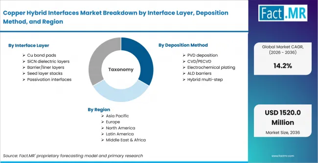
Copper Hybrid Interfaces Market Breakdown By Interface Layer, Deposition Method, And Region | Source: Fact.MR
| Attribute | Details |
|---|---|
| Quantitative Units | USD 402.0 million in 2026 to USD 1,520.0 million by 2036 at a 14.2% CAGR |
| Market Definition | Copper hybrid interfaces denotes the materials-and-equipment stack that forms the Cu-Cu half of a hybrid bond: CMP (dishing control), barrier/seed and plating for bond pads, surface activation, and the anneal furnaces that fuse recessed Cu pads into a void-free metallic joint - plus the inspection that verifies the interface. The market is defined by pad pitches already below 10 µm (vs. tens-of-µm solder-bump limits) and roadmaps toward sub-µm. |
| Interface Layer | Cu bond pads; SiCN dielectric layers; Barrier/liner layers; Seed layer stacks; Passivation interfaces |
| Deposition Method | PVD deposition; CVD/PECVD; Electrochemical plating; ALD barriers; Hybrid multi-step |
| Pad Pitch | <1 um; 1-3 um; 3-6 um; 6-10 um; >10 um |
| Application | HBM/DRAM stacks; Logic chiplets; Image sensors; Memory-on-logic; Photonics |
| End User | Memory manufacturers; Foundries; IDMs; OSAT providers; Materials R&D |
| Regions Covered | North America; Latin America; Europe; East Asia; South Asia & Oceania; Middle East & Africa |
| Countries Covered | South Korea; Taiwan; USA; Japan; Singapore |
| Key Companies Profiled | Applied Materials; Lam Research; Tokyo Electron; ASM International; Entegris; Resonac |
| Forecast Period | 2026 to 2036 |
| Approach | Hybrid top-down and bottom-up approach using demand indicators across Interface Layer; Deposition Method; Pad Pitch; Application; End User; country-level growth; company participation and adoption trends |
Source: Fact.MR analysis. Updated Jul 22, 2026
How is the market segmented?
-
By Interface Layer:
- Cu bond pads
- SiCN dielectric layers
- Barrier/liner layers
- Seed layer stacks
- Passivation interfaces
-
By Deposition Method:
- PVD deposition
- CVD/PECVD
- Electrochemical plating
- ALD barriers
- Hybrid multi-step
-
By Pad Pitch:
- <1 um
- 1-3 um
- 3-6 um
- 6-10 um
- >10 um
-
By Application:
- HBM/DRAM stacks
- Logic chiplets
- Image sensors
- Memory-on-logic
- Photonics
-
By End User:
- Memory manufacturers
- Foundries
- IDMs
- OSAT providers
- Materials R&D
-
By Region:
- North America
- Latin America
- Europe
- East Asia
- South Asia & Oceania
- Middle East & Africa
Frequently Asked Questions
Which Interface Layer leads the Copper Hybrid Interfaces Market?
Which Deposition Method leads the Copper Hybrid Interfaces Market?
Which Pad Pitch leads the Copper Hybrid Interfaces Market?
Which Application leads the Copper Hybrid Interfaces Market?
Which End User leads the Copper Hybrid Interfaces Market?
What CAGR is projected for South Korea in the Copper Hybrid Interfaces Market?
What CAGR is projected for USA in the Copper Hybrid Interfaces Market?
What CAGR is projected for Taiwan in the Copper Hybrid Interfaces Market?
What CAGR is projected for China in the Copper Hybrid Interfaces Market?
What CAGR is projected for Japan in the Copper Hybrid Interfaces Market?
What CAGR is projected for Singapore in the Copper Hybrid Interfaces Market?
What is the primary driver of the Copper Hybrid Interfaces Market?
What is the main restraint in the Copper Hybrid Interfaces Market?
Who worked on this report


Preview the report firsthand - request a free sample
Free SampleGet the brochure for pricing and purchase details
Download PDF