- Market Value (2025): USD 295.3 Mn
- Estimated Value (2026): USD 342.0 Mn
- Forecast Value (2036): USD 1480.0 Mn
- CAGR (2026-2036): 15.8%
What is the Queue-Time Hybrid Bonders Market forecast to be worth by 2036?
USD 342.0 million in 2026 to USD 1,480.0 million by 2036, at a 15.8% CAGR.
- The Queue-Time Hybrid Bonders Market crossed a valuation of USD 295.3 million in 2025, supported by demand from Memory manufacturers serving HBM/DRAM stacking workflows that require keeping plasma-activated dielectric and copper surfaces chemically ready while dies or wafers wait to be aligned.
- Demand is projected to increase from USD 342.0 million in 2026 to USD 1,480.0 million by 2036.
- The market is forecast to record a 15.8% CAGR from 2026 to 2036 as particle-controlled queue window, activated-surface decay and collective die-to-wafer flow remain central purchase reasons.
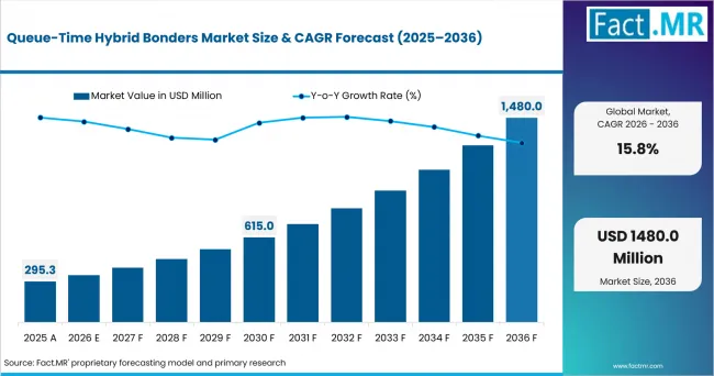
Queue Time Hybrid Bonders Market Value Analysis | Source: Fact.MR
What are the defining numbers behind Queue-Time Hybrid Bonders Market growth?
USD 1,138.0 million absolute opportunity is expected by 2036.
- Demand Drivers in the Market
- Particle-controlled queue window: Fabs are pushing bond-tool specifications toward tighter particle and atmosphere control because the interval between surface preparation and bond contact is itself a yield variable, not idle time; Semiconductor Engineering's review of hybrid bonding process flow confirms that surfaces are aligned and bonded within a short window after preparation, with the bond front then propagating at room temperature. [1]
- Activated-surface decay: Demand for atmosphere-controlled, in-bonder handling is rising because activated silicon surfaces react with air immediately; academic work on surface activation shows that bonding in a controlled nitrogen atmosphere preserves the surface reactivity that a longer queue time would otherwise destroy. [2]
- Collective die-to-wafer flow: Because die-to-wafer flows carry a structurally worse queue-time penalty than wafer-to-wafer bonding - each die waits while earlier dies are placed - buyers are shifting toward collective D2W (coD2W) architectures that place dies on a temporary carrier and bond them to the target wafer in a single step, collapsing the effective per-die queue time. [3]
- Cluster-integrated process sequence: Equipment vendors are answering this pressure by coupling plasma activation and megasonic/wet clean modules directly to the bond chamber, turning queue time into a robot-transfer interval measured in seconds rather than a lot-transfer delay measured in minutes to hours - a design shift Semiconductor Engineering ties to EV Group's and SUSS's differentiation on particle control and stability.
- Key Segments Analyzed
- By Bonder Configuration: Wafer-to-wafer bonders are projected to hold 34.0% share in 2026, supported by a clear process advantage: Wafer-to-wafer bonding brings the full wafer pair into contact in one coordinated event, so activated surfaces do not accumulate a die-by-die waiting penalty. That architecture is naturally compatible with cluster-integrated preparation and controlled mini-environments.
- By Queue-Time Control: Integrated vacuum transfer is projected to hold 48.1% share in 2026, supported by a clear process advantage: Integrated vacuum transfer keeps activated surfaces inside a controlled transfer chain from clean or plasma treatment to bond contact. The queue window becomes a measured robot handoff instead of an uncontrolled lot move through room air.
- By Bond Pitch: <1 um pitch is projected to hold 41.3% share in 2026, supported by a clear process advantage: At pitches below 1 micrometer, particles, copper oxide, pad recess and overlay error consume a larger fraction of the available contact margin. Queue-time control therefore becomes more valuable as interconnect density rises.
- By Application: HBM/DRAM stacking is projected to hold 37.9% share in 2026, supported by a clear process advantage: HBM and DRAM stacks multiply the number of bonded interfaces and place a high value on low-resistance, repeatable connections across every die in the stack. A queue-time excursion at one layer can impair the economics of the completed stack.
- By End User: Memory manufacturers are projected to hold 30.4% share in 2026, supported by a clear process advantage: Memory manufacturers are the earliest high-volume owners of hybrid-bonding recipes for HBM and vertically integrated memory. They control the full chain from wafer preparation through stack qualification, so the cost of queue-time drift appears directly in yield and throughput.
- Analyst Opinion at Fact.MR
- Shambhu Nath Jha, Sr. Consultant at Fact.MR, states, 'Buyers should evaluate the complete process sequence around keeping plasma-activated dielectric and copper surfaces chemically ready while dies or wafers wait to be aligned. Technical review should focus on repeatability, integration, defect control and production throughput rather than a single headline specification. Suppliers that connect tool performance to measurable yield and qualification results are likely to build trust faster.'
- Strategic Implications
- Buyers should compare the complete activation-to-contact sequence, including atmosphere, robot handoffs and queue-time traceability, rather than judging the bonder only by placement accuracy.
- Equipment suppliers should document how their systems address the challenge of keeping plasma-activated dielectric and copper surfaces chemically ready while dies or wafers wait to be aligned across production-representative wafers, panels, dies or packages.
- Procurement teams can compare process capability, integration burden, service coverage and qualification evidence before prioritizing nominal throughput or a single accuracy claim.
South Korea is projected to record a 17.4% CAGR as high-volume memory, HBM and vertically integrated semiconductor manufacturing supports relevant capital spending; Taiwan is projected to record a 17.0% CAGR as leading foundry production, advanced packaging and a dense OSAT and substrate supply chain supports relevant capital spending; USA is projected to record a 17.2% CAGR as leading-edge logic, high-performance computing, federally supported semiconductor R&D and a large domestic equipment base supports relevant capital spending; Japan is projected to record a 16.4% CAGR as semiconductor equipment, materials, inspection and memory-process expertise supports relevant capital spending; while Singapore is projected to record a 15.9% CAGR as advanced-packaging R&D, specialty fabs and regional assembly and test operations supports relevant capital spending through 2036.
How does the Queue-Time Hybrid Bonders Market break down by segment?
Wafer-to-wafer bonders leads Bonder Configuration with a 34.0% share, while Integrated vacuum transfer accounts for 48.1% of Queue-Time Control in 2026.
Why do Wafer-to-wafer bonders lead Bonder Configuration?
Wafer-to-wafer bonders are projected to account for 34.0% share in 2026.
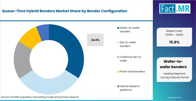
Queue Time Hybrid Bonders Market Analysis By Bonder Configuration | Source: Fact.MR
Wafer-to-wafer bonding brings the full wafer pair into contact in one coordinated event, so activated surfaces do not accumulate a die-by-die waiting penalty. That architecture is naturally compatible with cluster-integrated preparation and controlled mini-environments. Die-to-wafer bonding offers known-good-die flexibility, but sequential placement creates a longer and more variable time-to-contact unless the flow is converted to collective D2W. BIS added China-wide controls on advanced-packaging semiconductor manufacturing equipment (SME) alongside HBM controls; advanced hybrid-bonding equipment for China-bound advanced packaging falls inside the tightened regime, which directly affects where queue-time-optimized D2W bonders can be shipped without licenses. [5][6] Buyers therefore tend to treat wafer-to-wafer bonders as the practical choice when qualification must balance process capability, repeatability and production economics.
Why does Integrated vacuum transfer lead Queue-Time Control?
Integrated vacuum transfer is projected to account for 48.1% share in 2026.
Integrated vacuum transfer keeps activated surfaces inside a controlled transfer chain from clean or plasma treatment to bond contact. The queue window becomes a measured robot handoff instead of an uncontrolled lot move through room air. Inert-ambient handling reduces oxidation and moisture exposure, but separate modules and additional handoffs leave more opportunity for delay and particle adders. Tool vendors are collapsing the queue window by coupling plasma activation and megasonic/wet clean modules directly to the bond chamber, so the queue time becomes a robot-transfer time (seconds) rather than a lot-transfer time (minutes to hours). Semiconductor Engineering quotes both EV Group and SUSS on particle control and stability as the differentiators in this integrated regime. Buyers therefore tend to treat integrated vacuum transfer as the practical choice when qualification must balance process capability, repeatability and production economics.
Why does <1 um pitch lead Bond Pitch?
<1 um pitch is projected to account for 41.3% share in 2026.
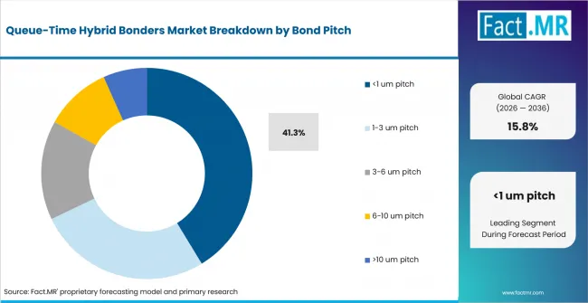
Queue Time Hybrid Bonders Market Analysis By Bond Pitch | Source: Fact.MR
At pitches below 1 micrometer, particles, copper oxide, pad recess and overlay error consume a larger fraction of the available contact margin. Queue-time control therefore becomes more valuable as interconnect density rises. The 1-3 micrometer class provides more geometric margin and can tolerate a less tightly integrated preparation-to-bond sequence. Semiconductor Engineering's review of hybrid bonding process flow notes that after surface preparation, following a short queue time (longer for die-to-wafer processes), the two wafers are aligned (using IR light) and brought into intimate contact, and that the bond front then propagates at room temperature. The article also quotes EV Group on in-situ process monitoring, air-flow management, and mini-environments to control particles during the queue/bond sequence - particle control during the waiting window is a yield variable, not a cosmetic one. [1] Buyers therefore tend to treat <1 um pitch as the practical choice when qualification must balance process capability, repeatability and production economics.
Why does HBM/DRAM stacking lead Application?
HBM/DRAM stacking is projected to account for 37.9% share in 2026.
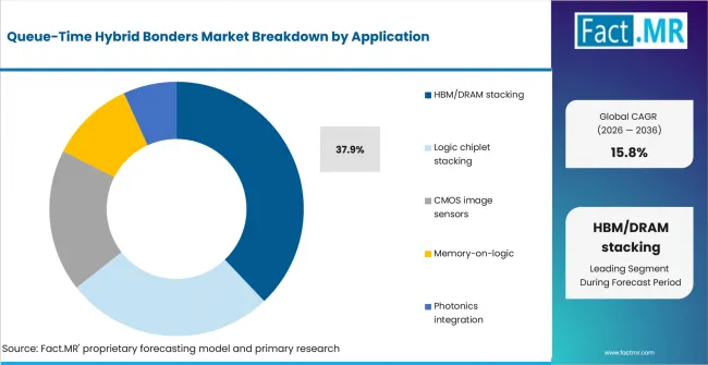
Queue Time Hybrid Bonders Market Analysis By Application | Source: Fact.MR
HBM and DRAM stacks multiply the number of bonded interfaces and place a high value on low-resistance, repeatable connections across every die in the stack. A queue-time excursion at one layer can impair the economics of the completed stack. Logic chiplet assembly is also demanding, but memory stacking combines high interface count with high-volume repetition, making time-to-bond control a more immediate production issue. Semiconductor Engineering notes face-to-back bonding processes are now available to stack more than two wafers - each additional layer multiplies the penalty of any queue-time-induced surface degradation, pushing queue-time control from a nicety to an architecture decision. Buyers therefore tend to treat HBM/DRAM stacking as the practical choice when qualification must balance process capability, repeatability and production economics.
Why do Memory manufacturers lead End User?
Memory manufacturers are projected to account for 30.4% share in 2026.
Memory manufacturers are the earliest high-volume owners of hybrid-bonding recipes for HBM and vertically integrated memory. They control the full chain from wafer preparation through stack qualification, so the cost of queue-time drift appears directly in yield and throughput. Foundries serve a broader device mix and may prioritize flexibility, whereas memory producers can standardize the sequence around repeated stack architectures. Academic work on surface activation shows that activated silicon surfaces react immediately when exposed to air, reducing bond strength, and that bonding in a controlled nitrogen atmosphere preserves surface reactivity - direct evidence that the environment during the queue window (O2, H2O exposure) degrades the activated surface and motivates in-bonder atmosphere control. [2] Buyers therefore tend to treat memory manufacturers as the practical choice when qualification must balance process capability, repeatability and production economics.
What is accelerating Queue-Time Hybrid Bonders Market adoption, and what is holding it back?
The strongest accelerator is particle-controlled queue window, while the main restraint is that long qualification cycles arise because surface chemistry, CMP condition, ambient exposure and placement throughput must be tuned as one process window.
Drivers Impact Analysis
| DRIVER | (~) % IMPACT ON CAGR | GEOGRAPHIC RELEVANCE | IMPACT TIMELINE |
|---|---|---|---|
| Particle-controlled queue window | +4.4% | Global leading-edge fabs | Medium term (2-4 years) |
| Activated-surface decay | +3.6% | Global leading-edge fabs | Medium term (2-4 years) |
| Collective die-to-wafer flow | +3.0% | Global leading-edge fabs | Short term (<=2 years) |
| Cluster-integrated process sequence | +2.4% | Global leading-edge fabs | Medium term (2-4 years) |
Source: Fact.MR analysis. Updated Jul 22, 2026
- Particle-controlled queue window: Semiconductor Engineering's review of hybrid bonding process flow notes that after surface preparation, following a short queue time (longer for die-to-wafer processes), the two wafers are aligned (using IR light) and brought into intimate contact, and that the bond front then propagates at room temperature. [1]
- Activated-surface decay: Academic work on surface activation shows that activated silicon surfaces react immediately when exposed to air, reducing bond strength, and that bonding in a controlled nitrogen atmosphere preserves surface reactivity - direct evidence that the environment during the queue window (O2, H2O exposure) degrades the activated surface and motivates in-bonder atmosphere control. [2]
- Collective die-to-wafer flow: For die-to-wafer (D2W) flows the queue-time problem is structurally worse than wafer-to-wafer: each die is activated/cleaned and then must wait while preceding dies are placed. This is the core argument for collective D2W (coD2W), in which dies are first placed on a temporary carrier and bonded to the target wafer in a single wafer-level step, collapsing the effective per-die queue time. [3]
- Cluster-integrated process sequence: Tool vendors are collapsing the queue window by coupling plasma activation and megasonic/wet clean modules directly to the bond chamber, so the queue time becomes a robot-transfer time (seconds) rather than a lot-transfer time (minutes to hours). Semiconductor Engineering quotes both EV Group and SUSS on particle control and stability as the differentiators in this integrated regime.
Opportunity Impact Analysis
| OPPORTUNITY | (~) % IMPACT ON CAGR | GEOGRAPHIC RELEVANCE | IMPACT TIMELINE |
|---|---|---|---|
| Collective D2W and face-to-back stacking | +2.7% | Global leading-edge fabs | Short term (<=2 years) |
| Copper recess/dishing specs tighten the window | +2.1% | Global leading-edge fabs | Medium term (2-4 years) |
| CHIPS Act / NAPMP | +1.6% | USA | Medium term (2-4 years) |
Source: Fact.MR analysis. Updated Jul 22, 2026
- Collective D2W and face-to-back stacking: Semiconductor Engineering notes face-to-back bonding processes are now available to stack more than two wafers - each additional layer multiplies the penalty of any queue-time-induced surface degradation, pushing queue-time control from a nicety to an architecture decision.
- Copper recess/dishing specs tighten the window: BESI (quoted in the same review) looks for up to 5 nm copper dishing from CMP; a recessed Cu pad that sits exposed to atmosphere during a long queue oxidizes, and copper-oxide interfacial layers show up later as elevated contact resistance or opens (see failure-analysis evidence below). [4]
- CHIPS Act / NAPMP: The US National Advanced Packaging Manufacturing Program's second NOFO (up to $1.6B) explicitly funds equipment, tools, processes, and process integration for advanced packaging including hybrid bonding (W2W, D2W) - a direct demand-side policy driver for US-installed bonding capacity. [7]
Restraints Impact Analysis
| RESTRAINT | (~) % IMPACT ON CAGR | GEOGRAPHIC RELEVANCE | IMPACT TIMELINE |
|---|---|---|---|
| Primary qualification constraint | -2.4% | Global leading-edge fabs | Medium term (2-4 years) |
| Contamination and defect risk | -1.9% | Global leading-edge fabs | Medium term (2-4 years) |
| Surface-state degradation | -1.4% | Global leading-edge fabs | Medium term (2-4 years) |
Source: Fact.MR analysis. Updated Jul 22, 2026
- Primary qualification constraint: Long qualification cycles arise because surface chemistry, CMP condition, ambient exposure and placement throughput must be tuned as one process window. [1]
- Contamination and defect risk: The article also quotes EV Group on in-situ process monitoring, air-flow management, and mini-environments to control particles during the queue/bond sequence - particle control during the waiting window is a yield variable, not a cosmetic one. [1]
- Surface-state degradation: Academic work on surface activation shows that activated silicon surfaces react immediately when exposed to air, reducing bond strength, and that bonding in a controlled nitrogen atmosphere preserves surface reactivity - direct evidence that the environment during the queue window (O2, H2O exposure) degrades the activated surface and motivates in-bonder atmosphere control. [2]
Which countries are scaling Queue-Time Hybrid Bonders Market fastest?
In USA, Queue Time Hybrid Bonders Market is projected to advance at 17.2% CAGR, supported by leading-edge logic, high-performance computing, federally supported semiconductor R&D and a large domestic equipment base.
- Countries differ less by the headline CAGR than by the type of semiconductor work creating demand for the Queue-Time Hybrid Bonders Market.
- South Korea follows a pathway shaped by high-volume memory, HBM and vertically integrated semiconductor manufacturing. USA takes a different path through leading-edge logic, high-performance computing, federally supported semiconductor R&D and a large domestic equipment base.
- Taiwan remain aligned through distinct combinations of device production, equipment development and advanced packaging investment.
- Japan develops through semiconductor equipment, materials, inspection and memory-process expertise, while Singapore relies on advanced-packaging R&D, specialty fabs and regional assembly and test operations.
- Markets with similar CAGRs can follow different development paths because installed fabs, device mix, local equipment capability, export controls and qualification cycles differ.
The full report compares the named country markets within the wider regional coverage of North America, Latin America, Europe, East Asia, South Asia & Oceania, and the Middle East & Africa.
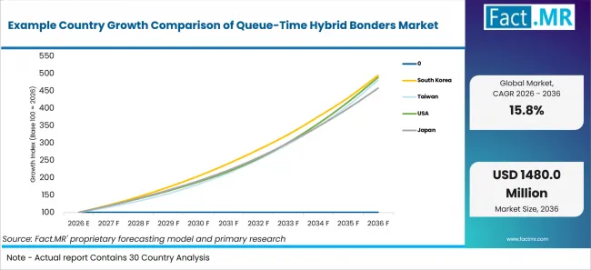
Example Country Growth Comparison Of Queue Time Hybrid Bonders Market | Source: Fact.MR
| COUNTRY | CAGR, 2026 to 2036 |
|---|---|
| South Korea | 17.4% |
| USA | 17.2% |
| Taiwan | 17.0% |
| Japan | 16.4% |
| Singapore | 15.9% |
Source: Fact.MR analysis. Updated Jul 22, 2026
What is driving South Korea's growth through 2036?
17.4% CAGR, supported by high-volume memory, HBM and vertically integrated semiconductor manufacturing.
South Korea combines high-volume memory, HBM and vertically integrated semiconductor manufacturing with a 43.0% share of 2026 demand across the six profiled countries. Tool vendors are collapsing the queue window by coupling plasma activation and megasonic/wet clean modules directly to the bond chamber, so the queue time becomes a robot-transfer time (seconds) rather than a lot-transfer time (minutes to hours). The commercial link is the need to solve the problem of keeping plasma-activated dielectric and copper surfaces chemically ready while dies or wafers wait to be aligned as capacity and process complexity increase.
What is driving USA's growth through 2036?
17.2% CAGR, supported by leading-edge logic, high-performance computing, federally supported semiconductor R&D and a large domestic equipment base.
USA combines leading-edge logic, high-performance computing, federally supported semiconductor R&D and a large domestic equipment base with a 12.9% share of 2026 demand across the six profiled countries. The US National Advanced Packaging Manufacturing Program's second NOFO (up to $1.6B) explicitly funds equipment, tools, processes, and process integration for advanced packaging including hybrid bonding (W2W, D2W) - a direct demand-side policy driver for US-installed bonding capacity. [7] The commercial link is the need to solve the problem of keeping plasma-activated dielectric and copper surfaces chemically ready while dies or wafers wait to be aligned as capacity and process complexity increase.
What is driving Taiwan's growth through 2036?
17.0% CAGR, supported by leading foundry production, advanced packaging and a dense OSAT and substrate supply chain.
Taiwan combines leading foundry production, advanced packaging and a dense OSAT and substrate supply chain with a 21.5% share of 2026 demand across the six profiled countries. BESI (quoted in the same review) looks for up to 5 nm copper dishing from CMP; a recessed Cu pad that sits exposed to atmosphere during a long queue oxidizes, and copper-oxide interfacial layers show up later as elevated contact resistance or opens (see failure-analysis evidence below). [4] The commercial link is the need to solve the problem of keeping plasma-activated dielectric and copper surfaces chemically ready while dies or wafers wait to be aligned as capacity and process complexity increase.
What is driving Japan's growth through 2036?
16.4% CAGR, supported by semiconductor equipment, materials, inspection and memory-process expertise.
Tokyo Electron integrates its Synapse bonding line with in-house plasma activation/clean; TEL also pairs bonding with its cryogenic etch franchise for NAND CMOS-under-array hybrid-bonded flows (peripheral CMOS wafer hybrid-bonded to the memory array, noted by Semiconductor Engineering). [8] This environment creates a clear qualification pathway for the Queue-Time Hybrid Bonders Market because buyers must solve the problem of keeping plasma-activated dielectric and copper surfaces chemically ready while dies or wafers wait to be aligned at production scale.
What is driving Singapore's growth through 2036?
15.9% CAGR, supported by advanced-packaging R&D, specialty fabs and regional assembly and test operations.
Singapore combines advanced-packaging R&D, specialty fabs and regional assembly and test operations with a 5.9% share of 2026 demand across the six profiled countries. For die-to-wafer (D2W) flows the queue-time problem is structurally worse than wafer-to-wafer: each die is activated/cleaned and then must wait while preceding dies are placed. [3] The commercial link is the need to solve the problem of keeping plasma-activated dielectric and copper surfaces chemically ready while dies or wafers wait to be aligned as capacity and process complexity increase.
Who leads the Queue-Time Hybrid Bonders Market?
EV Group and SUSS MicroTec lead the competitive landscape, followed by BESI and Applied Materials as the next tier of challengers.
EV Group participates through wafer bonding, activation and cluster-integrated process control. In-situ process monitoring, mini-environments, air-flow management, and distortion/feedback loops from metrology into the bonder (quoted via Semiconductor Engineering). SUSS MicroTec participates through wafer alignment, bonding and advanced-packaging lithography. Alignment <100 nm, in some cases <50 nm, with repeatability bond-to-bond emphasized (Thomas Schmidt, quoted in Semiconductor Engineering). BESI participates through high-accuracy die placement and hybrid-bonding assembly. Up to 5 nm dishing specs, Chameo Ultra Plus D2W platform, co-development with imec on overlay/residual-error modeling (pedestal-induced die scaling errors of ~80 nm documented). Applied Materials participates through deposition, etch, materials engineering and integrated process modules, with relevance determined by its ability to address the challenge of keeping plasma-activated dielectric and copper surfaces chemically ready while dies or wafers wait to be aligned.
Tokyo Electron holds a more specialized role through etch, clean, deposition and wafer-bonding process equipment, particularly where custom integration and service coverage affect qualification. Kulicke & Soffa holds a more specialized role through advanced die attach and packaging assembly, particularly where custom integration and service coverage affect qualification.
Competition is expected to center on repeatable process performance, integration with adjacent modules, installed-base service and documented capability to address the challenge of keeping plasma-activated dielectric and copper surfaces chemically ready while dies or wafers wait to be aligned. Buyers are likely to compare accuracy, defect prevention, throughput, recipe stability and the completeness of the delivered process cell.
Which companies are the key providers?
Key companies include EV Group; SUSS MicroTec; BESI; Applied Materials; Tokyo Electron; Kulicke & Soffa.
- EV Group
- SUSS MicroTec
- BESI
- Applied Materials
- Tokyo Electron
- Kulicke & Soffa
Bibliography
- [1] Semiconductor Engineering. (n.d.). Making Hybrid Bonding Better.
- [2] Athena. (n.d.). Uvn2 Paper.
- [3] IMAPS. (n.d.). 128385 Overlay Analysis And Optimization For High Accuracy Hybrid D2W Bonding.
- [4] Ninescrolls. (n.d.). Hybrid Bonding Failure Analysis.
- [5] U.S. Bureau of Industry and Security. (n.d.). Commerce Strengthens Export Controls to Restrict China's Capability to Produce Advanced Semiconductors for Military Applications.
- [6] Congressional Research Service / Congress.gov. (n.d.). R48642.4.
- [7] Performance.gov / U.S. Department of Commerce. (n.d.). Fy2024 Q3 Doc Progress Advance U.S. Semiconductor Manufacturing.
- [8] Semiconductor Engineering. (n.d.). Cryogenic Etch A Key Enabler Of 3D Nand.
This Report Addresses
- The report provides strategic intelligence on Queue-Time Hybrid Bonders Market across Bonder Configuration and Queue-Time Control choices that shape purchasing decisions.
- Segment analysis covers Wafer-to-wafer bonders as the share leader within the 2026 market structure.
- Regional outlook evaluates South Korea and Taiwan alongside USA and Japan, while Singapore completes the growth comparison.
- Competitive analysis profiles EV Group and SUSS MicroTec alongside BESI and Applied Materials, followed by additional active providers.
- Use-case assessment covers the categories and applications that shape demand in the Queue-Time Hybrid Bonders Market across the forecast period.
What does the Queue-Time Hybrid Bonders Market cover?
The market covers equipment and process systems configured to address the challenge of keeping plasma-activated dielectric and copper surfaces chemically ready while dies or wafers wait to be aligned.
Queue time in hybrid bonding is the maximum allowable elapsed time between surface preparation (plasma activation / final clean) and the moment the two bonding surfaces are brought into intimate contact. Queue-time hybrid bonders are bonders engineered to shrink, control, or relax this window - typically through integrated pre-bond modules (activation, cleaning, DI rinse, drying inside the bonder or in a directly coupled cluster), controlled atmospheres (N2 or vacuum mini-environments), and high-throughput architectures (collective die-to-wafer, coD2W) that limit how long an activated surface waits before bonding.
Commercial value arises from the complete configured system, including process control, handling, software and integrated modules required for repeatable operation. Finished semiconductor devices, package value and unrelated parent-market equipment are excluded.
What is included in the scope?
The scope includes systems used by memory manufacturers and the other end-user groups listed in the segmentation.
The market is segmented by Bonder Configuration, including Wafer-to-wafer bonders, Die-to-wafer bonders, Collective die-to-wafer, Panel-level bonders, Hybrid research platforms; Queue-Time Control, including Integrated vacuum transfer, Inert-ambient handling, Cluster-linked activation, Ambient-controlled staging, Timed-release scheduling; Bond Pitch, including <1 um pitch, 1-3 um pitch, 3-6 um pitch, 6-10 um pitch, >10 um pitch; Application, including HBM/DRAM stacking, Logic chiplet stacking, CMOS image sensors, Memory-on-logic, Photonics integration; End User, including Memory manufacturers, Foundries, OSAT providers, IDMs, R&D institutes.
Integrated handling, metrology, cleaning, activation, process-control or support modules are included when delivered as part of the configured market system.
What is excluded from the scope?
The scope excludes unrelated semiconductor equipment, standalone materials and components sold independently of the configured system.
It also excludes facility construction, cleanroom infrastructure, the value of processed wafers or packages, and adjacent process steps that are not part of the defined equipment category.
How Was the Analysis Built?
Fact.MR is of the opinion that this assessment combines structured market analysis with a review of public information and industry evidence relevant to the market.
- Market Assessment: The analysis considers demand patterns, supply conditions, segment mix, country activity, company participation, and adoption trends.
- Evidence Review: Public company disclosures, government and regulatory publications, trade information, technical literature, and industry records inform the assessment.
- Validation and Updates: Findings are cross-checked against available market indicators and reviewed when material market developments emerge.
Segmentation
What is the report's scope and coverage?
| Attribute | Details |
|---|---|
| Quantitative Units | USD 342.0 million in 2026 to USD 1,480.0 million by 2036 at a 15.8% CAGR |
| Market Definition | Queue time in hybrid bonding is the maximum allowable elapsed time between surface preparation (plasma activation / final clean) and the moment the two bonding surfaces are brought into intimate contact. |
| Bonder Configuration | Wafer-to-wafer bonders; Die-to-wafer bonders; Collective die-to-wafer; Panel-level bonders; Hybrid research platforms |
| Queue-Time Control | Integrated vacuum transfer; Inert-ambient handling; Cluster-linked activation; Ambient-controlled staging; Timed-release scheduling |
| Bond Pitch | <1 um pitch; 1-3 um pitch; 3-6 um pitch; 6-10 um pitch; >10 um pitch |
| Application | HBM/DRAM stacking; Logic chiplet stacking; CMOS image sensors; Memory-on-logic; Photonics integration |
| End User | Memory manufacturers; Foundries; OSAT providers; IDMs; R&D institutes |
| Regions Covered | North America; Latin America; Europe; East Asia; South Asia & Oceania; Middle East & Africa |
| Countries Covered | South Korea; Taiwan; USA; Japan; Singapore |
| Key Companies Profiled | EV Group; SUSS MicroTec; BESI; Applied Materials; Tokyo Electron; Kulicke & Soffa |
| Forecast Period | 2026 to 2036 |
| Approach | Hybrid top-down and bottom-up approach using demand indicators across Bonder Configuration; Queue-Time Control; Bond Pitch; Application; End User; country-level growth; company participation and adoption trends |
Source: Fact.MR analysis. Updated Jul 22, 2026
How is the market segmented?
-
By Bonder Configuration
- Wafer-to-wafer bonders
- Die-to-wafer bonders
- Collective die-to-wafer
- Panel-level bonders
- Hybrid research platforms
-
By Queue-Time Control
- Integrated vacuum transfer
- Inert-ambient handling
- Cluster-linked activation
- Ambient-controlled staging
- Timed-release scheduling
-
By Bond Pitch
- <1 um pitch
- 1-3 um pitch
- 3-6 um pitch
- 6-10 um pitch
- >10 um pitch
-
By Application
- HBM/DRAM stacking
- Logic chiplet stacking
- CMOS image sensors
- Memory-on-logic
- Photonics integration
-
By End User
- Memory manufacturers
- Foundries
- OSAT providers
- IDMs
- R&D institutes
-
By Region
- North America
- USA
- Latin America
- Other regional markets assessed at aggregate level
- Europe
- Other regional markets assessed at aggregate level
- East Asia
- South Korea
- Taiwan
- Japan
- South Asia & Oceania
- Singapore
- Middle East & Africa
- Other regional markets assessed at aggregate level
- North America
Frequently Asked Questions
Which Bonder Configuration leads the Queue-Time Hybrid Bonders Market?
Which Queue-Time Control leads the Queue-Time Hybrid Bonders Market?
Which Bond Pitch leads the Queue-Time Hybrid Bonders Market?
Which Application leads the Queue-Time Hybrid Bonders Market?
Which End User leads the Queue-Time Hybrid Bonders Market?
What CAGR is projected for South Korea in the Queue-Time Hybrid Bonders Market?
What CAGR is projected for USA in the Queue-Time Hybrid Bonders Market?
What CAGR is projected for Taiwan in the Queue-Time Hybrid Bonders Market?
What CAGR is projected for Japan in the Queue-Time Hybrid Bonders Market?
What CAGR is projected for Singapore in the Queue-Time Hybrid Bonders Market?
What is the primary driver of the Queue-Time Hybrid Bonders Market?
What is the main restraint in the Queue-Time Hybrid Bonders Market?
Who worked on this report


Preview the report firsthand - request a free sample
Free SampleGet the brochure for pricing and purchase details
Download PDF