- Market Value (2025): USD 316.3 Mn
- Estimated Value (2026): USD 358.0 Mn
- Forecast Value (2036): USD 1240.0 Mn
- CAGR (2026-2036):13.2%
What is the Die Placement Metrology Market forecast to be worth by 2036?
USD 358.0 million in 2026 to USD 1,240.0 million by 2036, at a 13.2% CAGR.
- The Die Placement Metrology Market crossed a valuation of USD 316.3 million in 2025, supported by demand from OSAT providers serving 2.5D interposer packages workflows that require separating placement error from die deformation, tool-stage error, substrate distortion and post-bond movement.
- Demand is projected to increase from USD 358.0 million in 2026 to USD 1,240.0 million by 2036.
- The market is forecast to record a 13.2% CAGR from 2026 to 2036 as accuracy classes, hybrid-bond requirements and error decomposition (the core of the metrology problem) remain central purchase reasons.
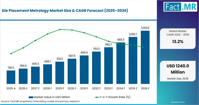
Die Placement Metrology Market Value Analysis | Source: Fact.MR
What are the defining numbers behind Die Placement Metrology Market growth?
USD 882.0 million absolute opportunity is expected by 2036.
- Demand Drivers in the Market
- Accuracy classes: Demand is stratifying by accuracy class as bonders themselves tighten their claims: R&D and prototyping die bonders now deliver reproducible sub-micron placement accuracy, automatic production flip-chip bonders advertise plus-or-minus 0.3 micrometer post-bond accuracy with leveling adjusted within 1 microradian, and university advanced-packaging lines specify plus-or-minus 0.5 micrometer X/Y and plus-or-minus 0.15 degree theta - each tier requiring metrology precise enough to verify it.
- Hybrid-bond requirements: Hybrid bonding is pulling metrology specs below 100 nm, and in some cases below 50 nm, with repeatability required bond to bond, while die-to-wafer machine-capability testing on a BESI Chameo Ultra Plus at imec demonstrated capability well below 200 nm at 3-sigma and under 200 nm residual worst-corner error on real test vehicles - benchmarks that buyers now specify against directly.
- Error decomposition (the core of the metrology problem): Because imec/BESI work has decomposed die-to-wafer placement error into correctable (X/Y/theta) versus non-correctable residuals - roughly 80 nm of die-corner scaling error from pedestal bending plus roughly 80 nm from dielectric/thickness mismatch, summing to about 110 nm when strong SiCN-SiCN bonding locks strain in - metrology tools that measure the full intra-die distortion field, rather than fiducial centroids alone, are increasingly the ones buyers specify.
- Thermal drift quantification: In thermocompression bonding at 250-400 degrees C, CTE mismatch drives positional drift beyond plus-or-minus 1-2 micrometer tolerances, and thermal radiation degrades vision-based measurement while mechanical stages drift with conducted heat, pushing demand toward metrology with built-in thermal compensation models and real-time correction.
- Key Segments Analyzed
- By Metrology Technique: Optical microscopy metrology is projected to hold 30.0% share in 2026, supported by a clear process advantage: Optical microscopy provides rapid, non-contact measurement of visible alignment marks over a wide field and fits naturally beside placement equipment. It supports frequent sampling without the acquisition time or shielding required by X-ray methods.
- By Measurement Stage: Post-placement is projected to hold 41.5% share in 2026, supported by a clear process advantage: Post-placement measurement isolates placement error before bonding heat, pressure or cure can move the die again. That timing allows the assembly cell to correct the next placement or reject a die while rework remains possible.
- By Accuracy Class: <0.5 um is projected to hold 40.2% share in 2026, supported by a clear process advantage: Accuracy below 0.5 micrometers provides margin for fine-pitch chiplets and high-density interposer connections after tool, mark and substrate uncertainties are combined. It also supports feedback rather than simple pass-fail inspection.
- By Package Type: 2.5D interposer packages are projected to hold 47.2% share in 2026, supported by a clear process advantage: A 2.5D interposer places several dies across a large, finely patterned routing surface, so local placement errors must be controlled without losing global package registration. The cost of a misplaced die rises because it can compromise an expensive interposer and neighboring chiplets.
- By End User: OSAT providers are projected to hold 29.5% share in 2026, supported by a clear process advantage: OSAT providers run diverse package formats and need metrology that can be reconfigured across customers while feeding placement equipment in production time. They also carry the assembly yield risk after receiving expensive known-good dies.
- Analyst Opinion at Fact.MR
- Shambhu Nath Jha, Sr. Consultant at Fact.MR, states, 'Buyers should evaluate the complete process sequence around separating placement error from die deformation, tool-stage error, substrate distortion and post-bond movement. Technical review should focus on repeatability, integration, defect control and production throughput rather than a single headline specification. Suppliers that connect tool performance to measurable yield and qualification results are likely to build trust faster.'
- Strategic Implications
- The useful specification is not an isolated best-case accuracy number; it is traceable pre- and post-bond error across the intended package and temperature window.
- Equipment suppliers should document how their systems address the challenge of separating placement error from die deformation, tool-stage error, substrate distortion and post-bond movement across production-representative wafers, panels, dies or packages.
- Procurement teams can compare process capability, integration burden, service coverage and qualification evidence before prioritizing nominal throughput or a single accuracy claim.
Taiwan is projected to record a 14.8% CAGR as leading foundry production, advanced packaging and a dense OSAT and substrate supply chain supports relevant capital spending; Malaysia is projected to record a 14.0% CAGR as large-scale outsourced assembly, test and package manufacturing supports relevant capital spending; South Korea is projected to record a 13.8% CAGR as high-volume memory, HBM and vertically integrated semiconductor manufacturing supports relevant capital spending; USA is projected to record a 14.7% CAGR as leading-edge logic, high-performance computing, federally supported semiconductor R&D and a large domestic equipment base supports relevant capital spending; while Japan is projected to record a 13.5% CAGR as semiconductor equipment, materials, inspection and memory-process expertise supports relevant capital spending through 2036.
How does the Die Placement Metrology Market break down by segment?
Optical microscopy metrology leads Metrology Technique with a 30.0% share, while Post-placement accounts for 41.5% of Measurement Stage in 2026.
Why does Optical microscopy metrology lead Metrology Technique?
Optical microscopy metrology is projected to account for 30.0% share in 2026.
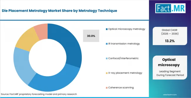
Die Placement Metrology Market Analysis By Metrology Technique | Source: Fact.MR
Optical microscopy provides rapid, non-contact measurement of visible alignment marks over a wide field and fits naturally beside placement equipment. It supports frequent sampling without the acquisition time or shielding required by X-ray methods. Infrared transmission is essential when marks are buried or obscured, but it depends more strongly on substrate transparency and material stack. Imec/BESI decomposed D2W placement error into correctable (X/Y/θ) vs non-correctable residuals: an ~80 nm die-corner scaling error caused by pedestal bending (tensile strain) plus ~80 nm from dielectric/thickness mismatch; with strong SiCN-SiCN bonding, strain locks in, summing to ~110 nm. Metrology must therefore measure intra-die distortion fields, rather than fiducial centroids alone. Buyers therefore tend to treat optical microscopy metrology as the practical choice when qualification must balance process capability, repeatability and production economics.
Why does Post-placement lead Measurement Stage?
Post-placement is projected to account for 41.5% share in 2026.
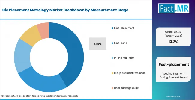
Die Placement Metrology Market Analysis By Measurement Stage | Source: Fact.MR
Post-placement measurement isolates placement error before bonding heat, pressure or cure can move the die again. That timing allows the assembly cell to correct the next placement or reject a die while rework remains possible. Post-bond metrology measures the final condition but cannot always distinguish placement error from movement created during bonding. Buyers therefore tend to treat post-placement as the practical choice when qualification must balance process capability, repeatability and production economics.
Why does <0.5 um lead Accuracy Class?
<0.5 um is projected to account for 40.2% share in 2026.
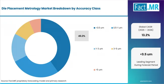
Die Placement Metrology Market Analysis By Accuracy Class | Source: Fact.MR
Accuracy below 0.5 micrometers provides margin for fine-pitch chiplets and high-density interposer connections after tool, mark and substrate uncertainties are combined. It also supports feedback rather than simple pass-fail inspection. The 0.5-1 micrometer class is adequate for many packages but becomes restrictive as pad pitch and overlay budgets tighten. W2W alignment must be even better than 100 nm, sometimes even 50 nm, and repeatable bond-to-bond (SUSS, via Semiconductor Engineering); D2W machine capability well below 200 nm @3σ on BESI Chameo Ultra Plus at imec, with <200 nm residual worst-corner error on real D2W test vehicles. Buyers therefore tend to treat <0.5 um as the practical choice when qualification must balance process capability, repeatability and production economics.
Why do 2.5D interposer packages lead Package Type?
2.5D interposer packages are projected to account for 47.2% share in 2026.
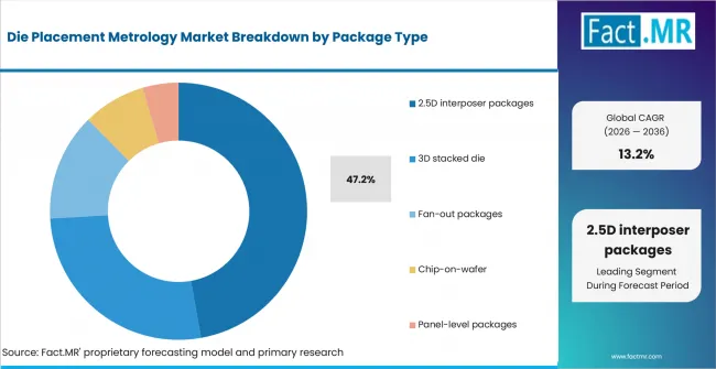
Die Placement Metrology Market Analysis By Package Type | Source: Fact.MR
A 2.5D interposer places several dies across a large, finely patterned routing surface, so local placement errors must be controlled without losing global package registration. The cost of a misplaced die rises because it can compromise an expensive interposer and neighboring chiplets. Three-dimensional stacks add depth and buried interfaces, but 2.5D interposers currently combine broad package area with high placement count. In TCB at 250-400 °C, CTE mismatch drives positional drift exceeding ±1-2 µm tolerances; thermal radiation degrades vision-based measurement, and mechanical stages drift with conducted heat - requiring thermal compensation models and real-time correction. Buyers therefore tend to treat 2.5D interposer packages as the practical choice when qualification must balance process capability, repeatability and production economics.
Why do OSAT providers lead End User?
OSAT providers are projected to account for 29.5% share in 2026.
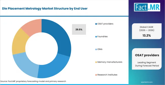
Die Placement Metrology Market Analysis By End User | Source: Fact.MR
OSAT providers run diverse package formats and need metrology that can be reconfigured across customers while feeding placement equipment in production time. They also carry the assembly yield risk after receiving expensive known-good dies. Foundries can integrate metrology with upstream process data, whereas OSATs require broader compatibility with incoming products and bonders. X-ray CT/laminography resolves die shift and alignment inside finished stacks: nano-CT with <100 nm voxels visualized 20 µm micro-bumps in an HBM stack (Nvidia GV100, 8-layer DRAM) and 1.5 µm hybrid Cu bonds at 9 µm pitch in an AMD 5800X3D - i.e., post-bond placement verification without cross-section. Buyers therefore tend to treat OSAT providers as the practical choice when qualification must balance process capability, repeatability and production economics.
What is accelerating Die Placement Metrology Market adoption, and what is holding it back?
The strongest accelerator is accuracy classes, while the main restraint is that sub-micron measurement can become the line bottleneck when field of view, optical access and calibration are not designed into the assembly cell.
Drivers Impact Analysis
| DRIVER | (~) % IMPACT ON CAGR | GEOGRAPHIC RELEVANCE | IMPACT TIMELINE |
|---|---|---|---|
| Accuracy classes | +3.7% | Global leading-edge fabs | Short term (<=2 years) |
| Hybrid-bond requirements | +3.0% | Global leading-edge fabs | Medium term (2-4 years) |
| Error decomposition (the core of the metrology problem) | +2.5% | Global leading-edge fabs | Medium term (2-4 years) |
| Thermal drift quantification | +2.0% | Global leading-edge fabs | Medium term (2-4 years) |
Source: Fact.MR analysis. Updated Jul 22, 2026
- Accuracy classes: R&D/prototyping die bonders deliver reproducible sub-micron placement accuracy (Finetech FINEPLACER sigma); automatic production flip-chip bonders advertise ±0.3 µm post-bond accuracy with leveling adjusted within 1 µradian (PicoTech); university advanced-packaging lines specify ±0.5 µm X/Y and ±0.15° theta.
- Hybrid-bond requirements: W2W alignment must be even better than 100 nm, sometimes even 50 nm, and repeatable bond-to-bond (SUSS, via Semiconductor Engineering); D2W machine capability well below 200 nm @3σ on BESI Chameo Ultra Plus at imec, with <200 nm residual worst-corner error on real D2W test vehicles.
- Error decomposition (the core of the metrology problem): Imec/BESI decomposed D2W placement error into correctable (X/Y/θ) vs non-correctable residuals: an ~80 nm die-corner scaling error caused by pedestal bending (tensile strain) plus ~80 nm from dielectric/thickness mismatch; with strong SiCN-SiCN bonding, strain locks in, summing to ~110 nm. Metrology must therefore measure intra-die distortion fields, rather than fiducial centroids alone.
- Thermal drift quantification: In TCB at 250-400 °C, CTE mismatch drives positional drift exceeding ±1-2 µm tolerances; thermal radiation degrades vision-based measurement, and mechanical stages drift with conducted heat - requiring thermal compensation models and real-time correction.
Opportunity Impact Analysis
| OPPORTUNITY | (~) % IMPACT ON CAGR | GEOGRAPHIC RELEVANCE | IMPACT TIMELINE |
|---|---|---|---|
| APC loops with litho scanners | +2.2% | Global leading-edge fabs | Medium term (2-4 years) |
| IR through-silicon alignment | +1.7% | Global leading-edge fabs | Medium term (2-4 years) |
| Split-axis bonder architectures | +1.3% | Global leading-edge fabs | Medium term (2-4 years) |
Source: Fact.MR analysis. Updated Jul 22, 2026
- APC loops with litho scanners: EV Group describes feedback loops between bonders and metrology/lithography tools - die placement metrology is becoming part of fab-wide APC, with incoming-wafer distortion maps forwarded to the bonder.
- IR through-silicon alignment: EVG SmartView face-to-face alignment (<200 nm 3σ) removes the need for IR-transparent substrates or backside marks - expanding measurable stacks.
Restraints Impact Analysis
| RESTRAINT | (~) % IMPACT ON CAGR | GEOGRAPHIC RELEVANCE | IMPACT TIMELINE |
|---|---|---|---|
| Primary qualification constraint | -2.0% | Global leading-edge fabs | Medium term (2-4 years) |
| Process-window sensitivity | -1.6% | Global leading-edge fabs | Medium term (2-4 years) |
| Buried-defect escape | -1.2% | Global leading-edge fabs | Medium term (2-4 years) |
Source: Fact.MR analysis. Updated Jul 22, 2026
- Primary qualification constraint: Sub-micron measurement can become the line bottleneck when field of view, optical access and calibration are not designed into the assembly cell.
- Process-window sensitivity: In TCB at 250-400 °C, CTE mismatch drives positional drift exceeding ±1-2 µm tolerances; thermal radiation degrades vision-based measurement, and mechanical stages drift with conducted heat - requiring thermal compensation models and real-time correction.
Which countries are scaling Die Placement Metrology Market fastest?
For Die Placement Metrology Market, South Korea's 13.8% CAGR reflects high-volume memory, HBM and vertically integrated semiconductor manufacturing.
- Countries differ less by the headline CAGR than by the type of semiconductor work creating demand for the Die Placement Metrology Market.
- China follows a pathway shaped by rapid domestic capacity build-out, local-equipment substitution and tighter access to controlled foreign tools. Taiwan takes a different path through leading foundry production, advanced packaging and a dense OSAT and substrate supply chain.
- USA and Malaysia remain aligned through distinct combinations of device production, equipment development and advanced packaging investment.
- South Korea develops through high-volume memory, HBM and vertically integrated semiconductor manufacturing, while Japan relies on semiconductor equipment, materials, inspection and memory-process expertise.
- Markets with similar CAGRs can follow different development paths because installed fabs, device mix, local equipment capability, export controls and qualification cycles differ.
The full report compares the six named country markets within the wider regional coverage of North America, Latin America, Europe, East Asia, South Asia & Oceania, and the Middle East & Africa.
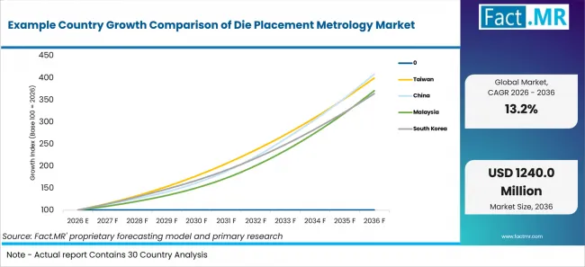
Example Country Growth Comparison Of Die Placement Metrology Market | Source: Fact.MR
| COUNTRY | CAGR, 2026 to 2036 |
|---|---|
| Taiwan | 14.8% |
| USA | 14.7% |
| Malaysia | 14.0% |
| South Korea | 13.8% |
| Japan | 13.5% |
Source: Fact.MR analysis. Updated Jul 22, 2026
What is driving Taiwan's growth through 2036?
14.8% CAGR, supported by leading foundry production, advanced packaging and a dense OSAT and substrate supply chain.
Taiwan combines leading foundry production, advanced packaging and a dense OSAT and substrate supply chain with a 37.9% share of 2026 demand across the six profiled countries. EVG SmartView face-to-face alignment (<200 nm 3σ) removes the need for IR-transparent substrates or backside marks - expanding measurable stacks. The commercial link is the need to solve the problem of separating placement error from die deformation, tool-stage error, substrate distortion and post-bond movement as capacity and process complexity increase.
What is driving USA's growth through 2036?
14.7% CAGR, supported by leading-edge logic, high-performance computing, federally supported semiconductor R&D and a large domestic equipment base.
K&S TC bonder split-axis; KLA/Onto extend wafer-overlay platforms to advanced packaging. This environment creates a clear qualification pathway for the Die Placement Metrology Market because buyers must solve the problem of separating placement error from die deformation, tool-stage error, substrate distortion and post-bond movement at production scale.
What is driving Malaysia's growth through 2036?
14.0% CAGR, supported by large-scale outsourced assembly, test and package manufacturing.
What is driving South Korea's growth through 2036?
13.8% CAGR, supported by high-volume memory, HBM and vertically integrated semiconductor manufacturing.
South Korea combines high-volume memory, HBM and vertically integrated semiconductor manufacturing with a 12.4% share of 2026 demand across the six profiled countries. The commercial link is the need to solve the problem of separating placement error from die deformation, tool-stage error, substrate distortion and post-bond movement as capacity and process complexity increase.
What is driving Japan's growth through 2036?
13.5% CAGR, supported by semiconductor equipment, materials, inspection and memory-process expertise.
TEL/Synapse integrated alignment; strong captive demand from HBM. This environment creates a clear qualification pathway for the Die Placement Metrology Market because buyers must solve the problem of separating placement error from die deformation, tool-stage error, substrate distortion and post-bond movement at production scale.
Which companies are the key providers?
Key companies include KLA; Onto Innovation; Camtek; Bruker; Nordson Test & Inspection; Zeiss.
- KLA
- Onto Innovation
- Camtek
- Bruker
- Nordson Test & Inspection
- Zeiss
Bibliography
- Finetech. (n.d.). Fineplacer Sigma.
- Picotech. (n.d.). Automatic Sub Micron Flip Chip Bonding.
- IMAPS. (n.d.). 128385 Overlay Analysis And Optimization For High Accuracy Hybrid D2W Bonding.
- Eureka. (n.d.). Report How To Align Die In Termocompression Bonding For Precision.
- Ieeetv. (n.d.). Metrology For Hybrid Bonds Microbumps And Tsvs In Advanced Packaging Are X Ray Methods Up To The Task.
- Nccavs Usergroups. (n.d.). Pag2010 7Pabo Rv.
- ASM International. (n.d.). High Resolution 3D X Ray Inspection For Advanced Packaging Insights From Hbm Micro Bump Analysis.
This Report Addresses
- The report provides strategic intelligence on Die Placement Metrology Market across Metrology Technique and Measurement Stage choices that shape purchasing decisions.
- Segment analysis covers Optical microscopy metrology as the share leader within the 2026 market structure.
- Regional outlook evaluates Taiwan and China along side Malaysia and South Korea, while USA and Japan complete the growth comparison.
- Competitive analysis profiles KLA and Onto Innovation alongside Camtek and Bruker, followed by additional active providers.
- Use-case assessment covers the categories and applications that shape demand in the Die Placement Metrology Market across the forecast period.
What does the Die Placement Metrology Market cover?
The market covers equipment and process systems configured to address the challenge of separating placement error from die deformation, tool-stage error, substrate distortion and post-bond movement.
Die placement metrology covers the measurement systems - in-bonder vision/IR systems, standalone post-bond overlay tools, and software APC loops - that quantify die-to-substrate placement error (X, Y, θ, Z-height/tilt, intra-die scaling and distortion) for flip-chip, thermocompression, and hybrid bonding. Distinct from general wafer overlay metrology, it must work on opaque, warped, sometimes IR-blocked assemblies and feed corrections back to bonders.
Commercial value arises from the complete configured system, including process control, handling, software and integrated modules required for repeatable operation. Finished semiconductor devices, package value and unrelated parent-market equipment are excluded.
What is included in the scope?
The scope includes systems used by osat providers and the other end-user groups listed in the segmentation.
The market is segmented by Metrology Technique, including Optical microscopy metrology, IR transmission metrology, Confocal/interferometric, X-ray placement metrology, Coherence scanning; Measurement Stage, including Post-placement, Post-bond, In-line real-time, Pre-placement reference, Final package audit; Accuracy Class, including <0.5 um, 0.5-1 um, 1-3 um, 3-5 um, >5 um; Package Type, including 2.5D interposer packages, 3D stacked die, Fan-out packages, Chip-on-wafer, Panel-level packages; End User, including OSAT providers, Foundries, IDMs, Memory manufacturers, Research institutes.
Integrated handling, metrology, cleaning, activation, process-control or support modules are included when delivered as part of the configured market system.
What is excluded from the scope?
The scope excludes unrelated semiconductor equipment, standalone materials and components sold independently of the configured system.
It also excludes facility construction, cleanroom infrastructure, the value of processed wafers or packages, and adjacent process steps that are not part of the defined equipment category.
How Was the Analysis Built?
Fact.MR is of the opinion that this assessment combines structured market analysis with a review of public information and industry evidence relevant to the market.
- Market Assessment: The analysis considers demand patterns, supply conditions, segment mix, country activity, company participation, and adoption trends.
- Evidence Review: Public company disclosures, government and regulatory publications, trade information, technical literature, and industry records inform the assessment.
- Validation and Updates: Findings are cross-checked against available market indicators and reviewed when material market developments emerge.
Segmentation
What is the report's scope and coverage?
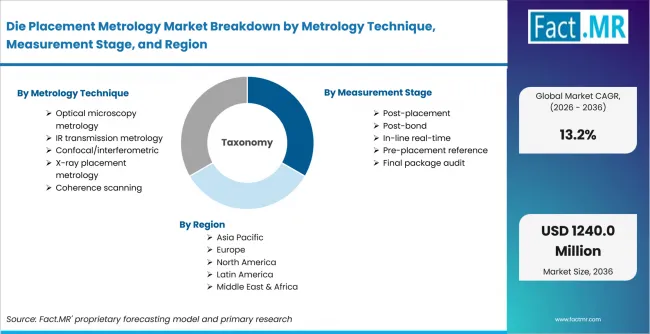
Die Placement Metrology Market Breakdown By Metrology Technique, Measurement Stage, And Region | Source: Fact.MR
| Attribute | Details |
|---|---|
| Quantitative Units | USD 358.0 million in 2026 to USD 1,240.0 million by 2036 at a 13.2% CAGR |
| Market Definition | Die placement metrology covers the measurement systems - in-bonder vision/IR systems, standalone post-bond overlay tools, and software APC loops - that quantify die-to-substrate placement error (X, Y, θ, Z-height/tilt, intra-die scaling and distortion) for flip-chip, thermocompression, and hybrid bonding. Distinct from general wafer overlay metrology, it must work on opaque, warped, sometimes IR-blocked assemblies and feed corrections back to bonders. |
| Metrology Technique | Optical microscopy metrology; IR transmission metrology; Confocal/interferometric; X-ray placement metrology; Coherence scanning |
| Measurement Stage | Post-placement; Post-bond; In-line real-time; Pre-placement reference; Final package audit |
| Accuracy Class | <0.5 um; 0.5-1 um; 1-3 um; 3-5 um; >5 um |
| Package Type | 2.5D interposer packages; 3D stacked die; Fan-out packages; Chip-on-wafer; Panel-level packages |
| End User | OSAT providers; Foundries; IDMs; Memory manufacturers; Research institutes |
| Regions Covered | North America; Latin America; Europe; East Asia; South Asia & Oceania; Middle East & Africa |
| Countries Covered | Taiwan; Malaysia; South Korea; USA; Japan |
| Key Companies Profiled | KLA; Onto Innovation; Camtek; Bruker; Nordson Test & Inspection; Zeiss |
| Forecast Period | 2026 to 2036 |
| Approach | Hybrid top-down and bottom-up approach using demand indicators across Metrology Technique; Measurement Stage; Accuracy Class; Package Type; End User; country-level growth; company participation and adoption trends |
Source: Fact.MR analysis. Updated Jul 22, 2026
How is the market segmented?
-
By Metrology Technique
- Optical microscopy metrology
- IR transmission metrology
- Confocal/interferometric
- X-ray placement metrology
- Coherence scanning
-
By Measurement Stage
- Post-placement
- Post-bond
- In-line real-time
- Pre-placement reference
- Final package audit
-
By Accuracy Class
- <0.5 um
- 0.5-1 um
- 1-3 um
- 3-5 um
- >5 um
-
By Package Type
- 2.5D interposer packages
- 3D stacked die
- Fan-out packages
- Chip-on-wafer
- Panel-level packages
-
By End User
- OSAT providers
- Foundries
- IDMs
- Memory manufacturers
- Research institutes
-
By Region
- North America
- USA
- Latin America
- Other regional markets assessed at aggregate level
- Europe
- Other regional markets assessed at aggregate level
- East Asia
- Taiwan
- South Korea
- Japan
- South Asia & Oceania
- Malaysia
- Middle East & Africa
- Other regional markets assessed at aggregate level
- North America
Frequently Asked Questions
Which Metrology Technique leads the Die Placement Metrology Market?
Which Measurement Stage leads the Die Placement Metrology Market?
Which Accuracy Class leads the Die Placement Metrology Market?
Which Package Type leads the Die Placement Metrology Market?
Which End User leads the Die Placement Metrology Market?
What CAGR is projected for Taiwan in the Die Placement Metrology Market?
What CAGR is projected for USA in the Die Placement Metrology Market?
What CAGR is projected for Malaysia in the Die Placement Metrology Market?
What CAGR is projected for South Korea in the Die Placement Metrology Market?
What CAGR is projected for Japan in the Die Placement Metrology Market?
What is the primary driver of the Die Placement Metrology Market?
What is the main restraint in the Die Placement Metrology Market?
Who worked on this report


Preview the report firsthand - request a free sample
Free SampleGet the brochure for pricing and purchase details
Download PDF