- Market Value (2025): USD 1.4 Bn
- Estimated Value (2026): USD 1.5 Bn
- Forecast Value (2036): USD 3.3 Bn
- CAGR (2026-2036): 8.2%
What is the Focused Ion Beam Market forecast to be worth by 2036?
USD 1.5 billion in 2026 to USD 3.3 billion by 2036 at 8.2% CAGR.
- The focused ion beam market crossed a valuation of USD 1.4 billion in 2025 as semiconductor labs kept funding cross-sectioning and sample-preparation work.
- Demand is projected to increase from USD 1.5 billion in 2026 to USD 3.3 billion by 2036 as failure review requires more precise milling.
- The market is forecast to record 8.2% CAGR from 2026 to 2036 owing to dense device structures and wider use of dual-beam platforms.
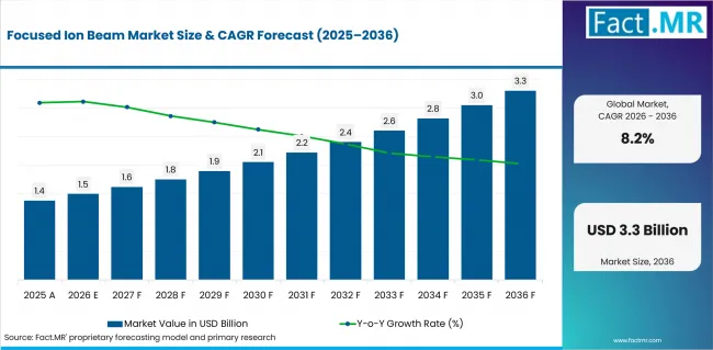
Focused Ion Beam Market Value Analysis | Source: Fact.MR
What are the defining numbers behind Focused Ion Beam Market growth?
USD 1.8 billion absolute opportunity by 2036, led by Ga+ Focused Ion Beam Systems and Semiconductor Failure Analysis alongside Semiconductor Manufacturers and Gallium Ion Source demand.
- Demand Drivers in the Market
- Semiconductor failure analysis requires milling accuracy that can expose buried defects without damaging the nearby structure. This makes FIB tools useful before imaging and circuit-edit decisions.
- Ga+ focused ion beam systems remain familiar to labs that need stable beam control and repeatable sample-preparation routines. Buyers approve these systems faster when training and service steps are clear.
- Materials science users need controlled cross-sectioning for metals and advanced device structures. This demand is selective, yet it supports orders outside high-volume semiconductor fabs.
- Direct sales channels matter when FIB purchases require demonstrations and installation planning. Suppliers that explain ownership cost and service response are better placed during procurement.
- Key Segments Analyzed
- By Product Type: Ga+ Focused Ion Beam Systems are expected to hold 36.7% share in 2026 since established workflows support buyer confidence.
- By Application: Semiconductor Failure Analysis is projected to account for 31.2% share in 2026 as chipmakers need cross-sectioning before defect review.
- By End User: Semiconductor Manufacturers are anticipated to capture 31.4% share in 2026 since device makers need FIB tools for process troubleshooting.
- By Distribution Channel: Direct Sales are estimated to represent 30.1% share in 2026 due to the need for demos and post-sale service planning.
- By Ion Source: Gallium Ion Source is forecast to hold 43.4% share in 2026 where routine milling depends on known beam behavior.
- Analyst Opinion at Fact.MR
- Shambhu Nath Jha, Senior Analyst at Fact.MR, states, “Focused ion beam suppliers need to prove more than tool precision. Buyers want evidence that the system can support failure analysis and service continuity after installation.”
- Strategic Implications
- Fab teams can link FIB selection with defect review before comparing quotes. This helps buyers check defects before approving production.
- Equipment providers can show how accurate milling improves imaging and film analysis. Clear performance proof can support later coating or filling processes.
- Investors need to separate direct FIB demand from packaging-related use. 3D semiconductor packaging matters when cross-sectioning helps improve yield or package reliability.
The USA is expected to record a 10.7% CAGR from 2026 to 2036 with fab qualification work and service-led purchasing. Japan is projected to record a 9.9% CAGR as reliability checks and compact lab workflows support demand. Germany is anticipated to grow at 9.1% through industrial research and semiconductor process validation. South Korea is estimated to post an 8.2% CAGR driven by memory users that need FIB support for defect review. Taiwan is forecast at 7.4% on the back of foundry activity and advanced device development. Canada is projected to reach 6.6% where research demand requires flexible sample-preparation tools. Singapore is expected to reach 5.7% with specialty fabs and compact technical support networks.
How does the Focused Ion Beam Market break down by segment?
Ga+ Focused Ion Beam Systems are expected to lead Product Type at 36.7% share in 2026. Semiconductor Failure Analysis is projected to lead Application at 31.2% share in 2026.
Which product type dominates?
Ga+ Focused Ion Beam Systems are projected to account for 36.7% share in 2026.
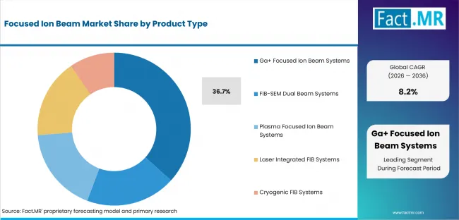
Focused Ion Beam Market Analysis By Product Type | Source: Fact.MR
Ga+ Focused Ion Beam Systems remain the leading product type because many laboratories already understand their performance and maintenance needs. Single Beam FIB Systems and High Current Ga+ FIB Systems serve buyers with different throughput requirements. FIB-SEM Dual Beam Systems attract users that prefer milling and imaging within the same platform.
What leads the Application segment?
Semiconductor Failure Analysis is expected to hold 31.2% share in 2026.
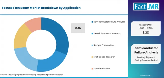
Focused Ion Beam Market Analysis By Application | Source: Fact.MR
Buried defects often need to be exposed before engineers can identify the cause of device failure. This requirement supports the use of FIB systems in Semiconductor Failure Analysis. Device Debugging and Circuit Edit support targeted changes to circuit features, while Materials Science Research creates demand where precise sample preparation is more important than processing speed.
How does End User shape demand?
Semiconductor Manufacturers are anticipated to lead with 31.4% share in 2026.
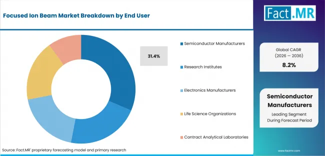
Focused Ion Beam Market Analysis By End User | Source: Fact.MR
Yield improvement places Semiconductor Manufacturers at the center of FIB demand. These companies use nanoscale milling to inspect defects and improve production processes. Integrated Device Manufacturers and Foundries rely on similar workflows for device qualification. Research Institutes also purchase FIB systems, although flexibility, training and experimental use have a greater influence on their buying decisions.
What supports Direct Sales within Distribution Channel?
Direct Sales are estimated to represent 30.1% share in 2026.
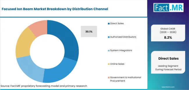
Focused Ion Beam Market Analysis By Distribution Channel | Source: Fact.MR
FIB systems usually require technical demonstrations and application testing before customers approve a purchase. As a result, Direct Sales remain the preferred channel. OEM Sales and Key Account Sales support large customers with established supplier relationships. Authorized Distributors become more important in markets where local installation, maintenance and technical support influence buyer confidence.
Why does Gallium Ion Source lead Ion Source?
Gallium Ion Source is forecast to hold 43.4% share in 2026.
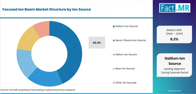
Focused Ion Beam Market Analysis By Ion Source | Source: Fact.MR
Many laboratories continue to select Gallium Ion Sources because their milling performance is well understood. Liquid Metal Ion Sources and High Brightness Ga Sources meet applications that require stronger resolution or beam stability. In comparison, Xenon Plasma Ion Sources are better suited to high-current milling where larger material areas need to be removed quickly.
What is accelerating Focused Ion Beam Market adoption, and what is holding it back?
Demand will rise with failure analysis and trusted Ga+ systems. High costs and long approval periods may limit adoption.
Drivers Impact Analysis
| DRIVER | QUALITATIVE RELEVANCE | GEOGRAPHIC RELEVANCE | IMPACT TIMELINE |
|---|---|---|---|
| Semiconductor failure analysis demand | High | USA, Japan, Taiwan | Short term (<= 2 years) |
| Ga+ workflow familiarity | High | USA, Germany, South Korea | Short term (<= 2 years) |
| Dual-beam milling and imaging | High | Semiconductor and research hubs | Medium term (2-4 years) |
| Materials research sample preparation | Moderate | Japan, Canada, Singapore | Medium term (2-4 years) |
| Direct sales and service support | Moderate | North America and East Asia | Long term (>= 4 years) |
Source: Fact.MR analysis. Updated Jul 29, 2026
- Semiconductor failure analysis demand: Device teams are expected to use FIB tools when buried defects must be exposed before imaging. This need supports repeat spending where yield learning depends on physical evidence.
- Ga+ workflow familiarity: Existing method knowledge reduces training risk for laboratories that already use gallium-based milling. Suppliers gain preference when familiar workflows come with dependable maintenance support.
- Dual-beam milling and imaging: Dual-beam platforms are expected to shorten review steps by combining material removal with immediate image feedback. This helps buyers justify the system when lab throughput is a concern.
- Materials research sample preparation: Research users need precise sectioning for complex materials and nanoscale structures. This creates selective demand outside semiconductor manufacturing when tool flexibility is more important than volume output.
- Direct sales and service support: High-value FIB purchases usually require demonstrations and service planning before approval. Direct supplier contact is expected to reduce purchase risk where uptime and application support decide acceptance.
Opportunity Impact Analysis
| OPPORTUNITY | QUALITATIVE RELEVANCE | GEOGRAPHIC RELEVANCE | IMPACT TIMELINE |
|---|---|---|---|
| FIB-SEM workflow integration | Moderate | USA and Japan | Medium term (2-4 years) |
| Advanced packaging failure review | Moderate | Taiwan and South Korea | Medium term (2-4 years) |
| Cryo FIB sample preparation | Moderate | Canada and research institutes | Long term (>= 4 years) |
| Local application support programs | Selective | Singapore and specialty fabs | Long term (>= 4 years) |
Source: Fact.MR analysis. Updated Jul 29, 2026
- FIB-SEM workflow integration: Suppliers that connect milling evidence with semiconductor metrology equipment can make tool approval easier. Buyers value platforms that reduce handoff delays between preparation and measurement.
- Advanced packaging failure review: Packaging teams need cross-section evidence when assembly defects appear after wafer processing. FIB systems are expected to gain value when they shorten the path from defect discovery to root-cause review.
- Cryo FIB sample preparation: Cryogenic workflows create opportunity where soft or beam-sensitive materials must be protected during milling. This route supports electron microscope use when prepared samples move into high-resolution imaging.
- Local application support programs: Smaller fabs and research labs are expected to approve purchases faster when training and troubleshooting are nearby. Service depth can decide whether a trial becomes a system order.
Restraints Impact Analysis
| RESTRAINT | QUALITATIVE RELEVANCE | GEOGRAPHIC RELEVANCE | IMPACT TIMELINE |
|---|---|---|---|
| High system and service cost | Moderate | Global | Short term (<= 2 years) |
| Long qualification and training cycle | Moderate | Semiconductor labs | Short term (<= 2 years) |
| Beam damage and preparation risk | Selective | Materials research users | Medium term (2-4 years) |
| Limited local support coverage | Selective | Canada, Singapore and smaller markets | Long term (>= 4 years) |
Source: Fact.MR analysis. Updated Jul 29, 2026
- High system and service cost: Focused ion beam platforms require large capital budgets and ongoing maintenance support. Smaller labs are expected to delay purchases when utilization is uncertain.
- Long qualification and training cycle: FIB tools need skilled operators and validated methods before routine use. Buyers may slow approvals when workflow transfer or application training takes too long.
- Beam damage and preparation risk: Sensitive samples can be affected when milling settings are not controlled carefully. This risk pushes buyers to ask for proof of preparation quality before expanding usage.
- Limited local support coverage: Service availability can become a barrier in markets with fewer installed systems. Procurement teams are expected to review response time and spare-part access before approving orders.
Which countries are scaling Focused Ion Beam Market fastest?
The country comparison is defined by a narrow growth spread. The total gap between the USA and Singapore is only 0.9 percentage points. The USA and Japan form the upper pair. Germany and South Korea remain close to the global rate. Taiwan follows through foundry demand. Canada and Singapore record steadier growth through research labs and specialty semiconductor activity.
- The USA records the highest listed CAGR as fab qualification work increases the need for failure analysis platforms. Service-led purchasing gives suppliers a clearer route to approval.
- Japan remains close to the USA through reliability-focused procurement and compact laboratory workflows. Buyers place more weight on proof that systems can support repeat sample preparation.
- Germany tracks the global pace through industrial research and semiconductor validation. Suppliers must show application depth before wider approvals.
- South Korea holds a measured position through memory manufacturing and equipment service needs. Tool acceptance depends on stable milling and fast support.
- Taiwan follows through foundry scale and advanced device development. Demand is expected to move where FIB systems shorten failure review and support process transfer.
- Canada and Singapore remain below the upper group where demand is more selective. Research institutes and specialty fabs are likely to prioritize flexibility and local support.
Comparable CAGRs can produce different market entry conditions across these countries. Deployment timing depends on application evidence and local service depth. Commercial readiness reflects buyer confidence in milling accuracy and uptime.
The full report provides country-level CAGR analysis across North America; Latin America; Europe; East Asia; South Asia; Oceania; and the Middle East and Africa.
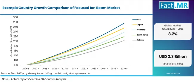
Example Country Growth Comparison Of Focused Ion Beam Market | Source: Fact.MR
| Country | CAGR (2026-2036) |
|---|---|
| USA | 10.7% |
| Japan | 9.9% |
| Germany | 9.1% |
| South Korea | 8.2% |
| Taiwan | 7.4% |
| Canada | 6.6% |
| Singapore | 5.7% |
Source: Fact.MR analysis. Updated Jul 29, 2026
What supports USA adoption?
10.7% CAGR, supported by fab qualification work and service-led purchasing.
USA buyers evaluate application proof before approving new FIB tools. Local demand is expected to grow where failure analysis teams need fast cross-section evidence before process decisions. Suppliers that show installation planning and maintenance response are better placed during high-value purchases.
How is Japan building demand?
9.9% CAGR, driven by reliability checks and compact lab workflows.
Japan’s compact laboratory base places more weight on repeatable preparation quality. Buyers are expected to favor systems that combine stable milling with dependable training support. Service clarity reduces disruption because smaller workspaces leave less room for workflow errors.
What keeps Germany aligned with the global rate?
9.1% CAGR, backed by industrial research and semiconductor validation.
Germany’s industrial research base keeps FIB approval tied to measured performance. Focused ion beam systems are expected to gain preference when suppliers prove sample-preparation accuracy and operator training. Procurement teams are likely to ask for service accountability before approval.
How is South Korea developing demand?
8.2% CAGR, supported by memory manufacturing and equipment service needs.
South Korea’s memory users need dependable FIB workflows for defect review and process learning. Equipment acceptance is expected to depend on milling stability and technical support. Clear fit with existing fab routines can shorten evaluation time.
What shapes Taiwan’s adoption route?
7.4% CAGR, driven by foundry activity and advanced device development.
Taiwan’s foundry activity creates demand for fast physical evidence during failure review. Suppliers can gain acceptance when FIB systems shorten troubleshooting cycles. The best route is expected to combine sample-preparation proof with support for process transfer.
How does Canada perform?
6.6% CAGR, led by research demand and service coverage needs.
Canada’s research demand is selective due to its spread-out user base. Buyers are expected to prioritize flexible sample-preparation capability and reliable service coverage. Purchase timing may depend on whether the system can serve more than one lab workflow.
What supports Singapore’s growth?
5.7% CAGR, backed by specialty fabs and compact technical support networks.
Singapore’s compact semiconductor cluster gives suppliers a practical support route. Specialty fabs and laboratories are likely to favor FIB systems that support stable recipes and efficient changeovers. Training access can help smaller teams approve tools with less risk.
Who leads the Focused Ion Beam Market?
Thermo Fisher Scientific and Carl Zeiss AG show the direct relevance. Hitachi High-Tech Corporation and JEOL Ltd. strengthen the wider FIB-SEM and electron microscopy landscape.
Thermo Fisher Scientific supports focused ion beam demand through dual-beam and sample-preparation platforms. Carl Zeiss AG contributes FIB-SEM capability for materials and semiconductor research. Hitachi High-Tech Corporation and JEOL Ltd. add electron microscopy depth that supports imaging-led analysis. TESCAN GROUP; Raith GmbH broaden the provider field through ion-beam and research-tool experience.
From 2026 to 2036, competition will depend on beam stability and technical support. Providers that support precise milling before imaging may gain stronger demand from semiconductor and nanotechnology users.
Which companies are the key providers?
Companies include Thermo Fisher Scientific; Carl Zeiss AG; Hitachi High-Tech Corporation; JEOL Ltd.; TESCAN GROUP; and Raith GmbH.
- Thermo Fisher Scientific
- Carl Zeiss AG
- Hitachi High-Tech Corporation
- JEOL Ltd.
- TESCAN GROUP
- Raith GmbH
Bibliography
- U.S. Department of Commerce. (2025, January 16). U.S. Department of Commerce announces $1.4 billion in final awards to support the next generation of U.S. semiconductor advanced packaging.
- Singapore Economic Development Board. (2025, March 7). Singapore semiconductor companies, including start-ups, can access new S$500 million national fabrication facility by 2027.
- Innovation, Science and Economic Development Canada. (2025, November 28). Canada invests in the semiconductor sector in partnership with IBM Canada and C2MI.
- Thermo Fisher Scientific Inc. (2025, October 6). Faster time to data in the fab with multi-ion species plasma FIB.
- TESCAN Group. (2025, September 1). AMBER X 2 wins 2025 R&D 100 Award for plasma FIB-SEM innovation.
This Report Answers
- The report provides strategic intelligence on the Focused Ion Beam Market across Product Type and Application choices that shape FIB purchasing and lab deployment.
- Segment analysis covers Ga+ Focused Ion Beam Systems and Semiconductor Failure Analysis as the share leaders within the 2026 market.
- Country outlook evaluates the USA and Japan alongside Germany and South Korea. Taiwan, Canada and Singapore complete the growth comparison across the profiled markets.
- Competitive analysis profiles Thermo Fisher Scientific and Carl Zeiss AG alongside Hitachi High-Tech Corporation and JEOL Ltd. TESCAN GROUP; Raith GmbH complete the provider set.
- Application assessment covers semiconductor failure analysis and sample preparation. Circuit edit, materials research and the integrated circuit market complete the adjacent use-case view.
What does the Focused Ion Beam Market cover?
Focused ion beam systems are used for controlled milling and sample preparation where nanoscale accuracy determines review quality.
The Focused Ion Beam Market covers equipment used in semiconductor failure analysis and device debugging. Coverage extends to FIB-SEM dual-beam tools and plasma FIB systems where milling and imaging support the same workflow. Life science and cryo-electron microscopy use cases are included when ion-beam sample preparation is required.
The market differs from general electron microscopy since commercial value comes from ion-beam milling and controlled material removal. General imaging-only equipment remains outside the boundary. Unrelated wet processing and broad lab instruments are excluded unless they directly support FIB sample preparation.
What is included in the scope?
Focused ion beam systems are used across semiconductor manufacturers and foundries. Research institutes and materials testing laboratories are included.
The scope includes Product Type and Application alongside End User, Distribution Channel and Ion Source. Coverage spans Ga+ systems and dual-beam platforms. Plasma FIB systems and cryogenic FIB variants are included. The scope also includes circuit edit and TEM lamella preparation when purchase decisions depend on focused ion beam capability.
What is excluded from the scope?
General laboratory equipment and unrelated semiconductor processing tools remain outside the scope of this market.
The scope excludes systems that do not use focused ion beam capability for milling or sample preparation. Standalone SEM systems are excluded unless demand is tied to FIB-SEM workflows. General deposition and packaging spending remain outside the scope unless directly tied to focused ion beam qualification or use.
How Was the Analysis Built?
The analysis draws on 120+ sources, 35+ company portfolios, 25+ countries, and more than 20 industry interviews.
- Primary Research: Primary research includes discussions with manufacturers, service providers, technology developers, distributors, end users, procurement teams, and subject-matter experts. These conversations examine purchasing priorities, product adoption, operational challenges, approval requirements, competitive positioning, and the factors that influence wider market acceptance.
- Desk Research: Desk research covers government statistics, regulatory publications, company filings, trade data, technical studies, industry associations, standards, public policy, and other authoritative sources. Every source used in the analysis is documented in the bibliography.
- Market Sizing and Forecasting: Market estimates combine historical performance, demand indicators, pricing and volume trends, segment shares, company participation, country-level growth, adoption patterns, investment activity, and barriers to market expansion.
- Data Validation and Update Cycle: Findings are validated by comparing primary interviews with public data, company activity, regulatory changes, trade patterns, and industry developments. Regular updates review new product launches, capacity changes, partnerships, approvals, procurement trends, and shifts in commercial adoption.
Segmentation
What is the report’s scope and coverage?
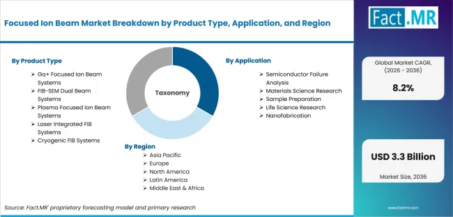
Focused Ion Beam Market Breakdown By Product Type, Application, And Region | Source: Fact.MR
| Attribute | Details |
|---|---|
| Quantitative Units | USD billion in 2026 to USD billion by 2036 at CAGR |
| Market Definition | Focused ion beam systems used for site-specific milling, cross-sectioning, circuit edit, sample preparation and nanoscale imaging support |
| Product Type | Ga+ Focused Ion Beam Systems; Single Beam FIB Systems; High Current Ga+ FIB Systems; FIB-SEM Dual Beam Systems; Gallium FIB-SEM Systems; Plasma FIB-SEM Systems; Plasma Focused Ion Beam Systems; Xenon Plasma FIB Systems; Oxygen Plasma FIB Systems; Laser Integrated FIB Systems; Femtosecond Laser FIB Systems; Nanosecond Laser FIB Systems; Cryogenic FIB Systems; Cryo FIB Milling Systems; Cryo FIB-SEM Systems |
| Application | Semiconductor Failure Analysis; Device Debugging; Circuit Edit; Materials Science Research; Microstructure Analysis; Nanomaterial Characterization; Sample Preparation; TEM Lamella Preparation; Cross-Section Preparation; Life Science Research; Cryo-Electron Microscopy; Biological Sample Milling; Nanofabrication; Prototype Fabrication; Nanopatterning |
| End User | Semiconductor Manufacturers; Integrated Device Manufacturers; Foundries; Research Institutes; Government Laboratories; Academic Institutions; Electronics Manufacturers; Microelectronics Companies; Advanced Packaging Companies; Life Science Organizations; Biotechnology Companies; Pharmaceutical Research Centers; Contract Analytical Laboratories; Materials Testing Laboratories; Commercial Research Service Providers |
| Distribution Channel | Direct Sales; OEM Sales; Key Account Sales; Authorized Distributors; Regional Distributors; Value-Added Resellers; System Integrators; Research Equipment Integrators; Semiconductor Equipment Integrators; Online Sales; Manufacturer Portals; B2B E-Commerce Platforms; Government & Institutional Procurement; Public Research Tenders; Academic Procurement Programs |
| Ion Source | Gallium Ion Source; Liquid Metal Ion Source; High Brightness Ga Source; Xenon Plasma Ion Source; High Current Xenon Source; Large Area Milling Source; Helium Ion Source; High Resolution Imaging; Surface Analysis Source; Neon Ion Source; Nanofabrication Source; High Precision Milling Source; Other Ion Sources; Oxygen Ion Source; Argon Ion Source |
| Regions Covered | North America; Latin America; Europe; East Asia; South Asia and Oceania; Middle East and Africa |
| Countries Covered | USA; Japan; Germany; South Korea; Taiwan; Canada; Singapore |
| Key Companies Profiled | Thermo Fisher Scientific; Carl Zeiss AG; Hitachi High-Tech Corporation; JEOL Ltd.; TESCAN GROUP; Raith GmbH |
| Forecast Period | 2026 to 2036 |
| Approach | Hybrid top-down and bottom-up approach using semiconductor equipment demand; failure analysis workloads; FIB-SEM adoption; sample-preparation requirements; ion-source selection; direct sales activity; service coverage; country adoption patterns and company portfolio review |
Source: Fact.MR analysis. Updated Jul 29, 2026
How is the market segmented?
-
By Product Type:
- Ga+ Focused Ion Beam Systems
- Single Beam FIB Systems
- High Current Ga+ FIB Systems
- FIB-SEM Dual Beam Systems
- Gallium FIB-SEM Systems
- Plasma FIB-SEM Systems
- Plasma Focused Ion Beam Systems
- Xenon Plasma FIB Systems
- Oxygen Plasma FIB Systems
- Laser Integrated FIB Systems
- Femtosecond Laser FIB Systems
- Nanosecond Laser FIB Systems
- Cryogenic FIB Systems
- Cryo FIB Milling Systems
- Cryo FIB-SEM Systems
-
By Application:
- Semiconductor Failure Analysis
- Device Debugging
- Circuit Edit
- Materials Science Research
- Microstructure Analysis
- Nanomaterial Characterization
- Sample Preparation
- TEM Lamella Preparation
- Cross-Section Preparation
- Life Science Research
- Cryo-Electron Microscopy
- Biological Sample Milling
- Nanofabrication
- Prototype Fabrication
- Nanopatterning
-
By End User:
- Semiconductor Manufacturers
- Integrated Device Manufacturers
- Foundries
- Research Institutes
- Government Laboratories
- Academic Institutions
- Electronics Manufacturers
- Microelectronics Companies
- Advanced Packaging Companies
- Life Science Organizations
- Biotechnology Companies
- Pharmaceutical Research Centers
- Contract Analytical Laboratories
- Materials Testing Laboratories
- Commercial Research Service Providers
-
By Distribution Channel:
- Direct Sales
- OEM Sales
- Key Account Sales
- Authorized Distributors
- Regional Distributors
- Value-Added Resellers
- System Integrators
- Research Equipment Integrators
- Semiconductor Equipment Integrators
- Online Sales
- Manufacturer Portals
- B2B E-Commerce Platforms
- Government & Institutional Procurement
- Public Research Tenders
- Academic Procurement Programs
-
By Ion Source:
- Gallium Ion Source
- Liquid Metal Ion Source
- High Brightness Ga Source
- Xenon Plasma Ion Source
- High Current Xenon Source
- Large Area Milling Source
- Helium Ion Source
- High Resolution Imaging
- Surface Analysis Source
- Neon Ion Source
- Nanofabrication Source
- High Precision Milling Source
- Other Ion Sources
- Oxygen Ion Source
- Argon Ion Source
-
By Region:
- North America
- Latin America
- Europe
- East Asia
- South Asia and Oceania
- Middle East and Africa
Frequently Asked Questions
Which Product Type leads the market?
Which Application leads the market?
Which End User leads the market?
Which Distribution Channel leads the market?
Which Ion Source leads the market?
Which country records the highest listed CAGR?
What is the primary driver in this market?
What is the main restraint?
Why do Semiconductor Manufacturers lead demand?
Who worked on this report


Preview the report firsthand - request a free sample
Free SampleGet the brochure for pricing and purchase details
Download PDF