- Market Value (2025): USD 774.6 Mn
- Estimated Value (2026): USD 880.0 Mn
- Forecast Value (2036): USD 3150.0 Mn
- CAGR (2026-2036): 13.6%
What is the GAA Epitaxy Systems Market forecast to be worth by 2036?
USD 880.0 million in 2026 to USD 3,150.0 million by 2036, at a 13.6% CAGR.
- The GAA Epitaxy Systems Market crossed a valuation of USD 774.6 million in 2025, supported by demand from Foundries serving 2 nm class workflows that require growing highly uniform Si/SiGe nanosheet stacks and selective source-drain structures with abrupt interfaces and minimal defects.
- Demand is projected to increase from USD 880.0 million in 2026 to USD 3,150.0 million by 2036.
- The market is forecast to record a 13.6% CAGR from 2026 to 2036 as the two epi modules in gaa, equipment-criticality list (tel) and why sige s/d epi matters electrically remain central purchase reasons.
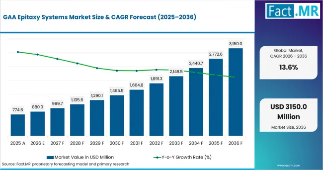
Gaa Epitaxy Systems Market Value Analysis | Source: Fact.MR
What are the defining numbers behind GAA Epitaxy Systems Market growth?
USD 2,270.0 million absolute opportunity is expected by 2036.
- Demand Drivers in the Market
- The two epi modules in GAA: Demand for GAA epitaxy tools is anchored in two distinct process modules: stacked nanosheet formation, where a SiGe/Si stack is epitaxially grown on the silicon substrate with high-precision per-layer thickness control, and source/drain formation, where n-type or p-type epitaxial layers are selectively grown on either side of the exposed nanosheet ends after inner-spacer formation, each module requiring dedicated tool capability.
- Equipment-criticality list (TEL): Toolmaker requirement documents are making epitaxy the named first module in the GAA flow: Tokyo Electron's own investor-relations deck lists defect-free, uniform SiGe/Si epitaxy for the mold stack alongside low-k inner-spacer deposition, highly selective SiGe etch for channel release, collapse-free drying, and conformal work-function-metal/dipole films, putting epitaxy quality at the top of the equipment-criticality list.
- Why SiGe S/D epi matters electrically: Demand for precision SiGe source/drain epitaxy is grounded in a measurable electrical payoff: selective SiGe growth in recessed S/D cavities induces compressive strain that boosts hole mobility by a documented 40-100% across MIT/IIT Bombay study data, with in-situ boron doping at 1-3x10^20 per cubic centimeter combining strain and conductivity gains in p-type nanosheet FETs.
- Critical-thickness constraint: Equipment precision requirements are tightening because SiGe must stay below critical thickness to avoid misfit dislocations and strain relaxation, a constraint that is getting harder to meet as nanosheet architectures limit S/D volume by inner-spacer dimensions and nanosheet pitch, a problem IBM patents specifically address through dislocation-free pseudomorphic growth across the full S/D volume.
- Key Segments Analyzed
- By Epitaxy Process: SiGe superlattice growth is projected to hold 33.0% share in 2026, supported by a clear process advantage: SiGe superlattice growth creates the alternating channel and sacrificial layers that define stacked nanosheets. Thickness, germanium fraction and interface abruptness are repeated many times, making epitaxy a structural device-forming step rather than a simple film deposition.
- By Reactor Type: Single-wafer reactors are projected to hold 42.6% share in 2026, supported by a clear process advantage: Single-wafer reactors provide rapid recipe transitions and tight control of temperature, composition and interface timing for complex multilayer stacks. They also isolate a process excursion to one wafer and support cluster integration with pre-clean.
- By Node Application: 2 nm class is projected to hold 41.4% share in 2026, supported by a clear process advantage: The 2 nanometer class is positioned as the next broad expansion of GAA logic and requires multiple selective epitaxy steps per wafer. Its expected foundry and IDM ramps create the largest near-term tool qualification and capacity workload in the market estimates.
- By Material System: SiGe alloys are projected to hold 44.1% share in 2026, supported by a clear process advantage: SiGe alloys provide strain engineering and selective etch contrast between sacrificial and silicon channel layers. Precise germanium composition is therefore central to both device performance and later nanosheet release.
- By End User: Foundries are projected to hold 31.2% share in 2026, supported by a clear process advantage: Foundries must offer GAA nodes across multiple customer designs and therefore invest heavily in reactor matching, process windows and yield learning. Epitaxy uniformity becomes part of a platform promise rather than a single internal product recipe.
- Analyst Opinion at Fact.MR
- Shambhu Nath Jha, Sr. Consultant at Fact.MR, states, 'Buyers should evaluate the complete process sequence around growing highly uniform Si/SiGe nanosheet stacks and selective source-drain structures with abrupt interfaces and minimal defects. Technical review should focus on repeatability, integration, defect control and production throughput rather than a single headline specification. Suppliers that connect tool performance to measurable yield and qualification results are likely to build trust faster.'
- Strategic Implications
- Fabs should evaluate composition control, thickness uniformity, selectivity, in-situ cleaning and integration with spacer and etch modules.
- Equipment suppliers should document how their systems address the challenge of growing highly uniform Si/SiGe nanosheet stacks and selective source-drain structures with abrupt interfaces and minimal defects across production-representative wafers, panels, dies or packages.
- Procurement teams should assess epitaxial thickness and composition uniformity, stress control, defect density, in-situ metrology, wafer throughput and reactor-service support.
Taiwan is projected to record a 15.0% CAGR as leading foundry production, advanced packaging and a dense OSAT and substrate supply chain supports relevant capital spending; USA is projected to record a 15.1% CAGR as leading-edge logic, high-performance computing, federally supported semiconductor R&D and a large domestic equipment base supports relevant capital spending; South Korea is projected to record a 14.5% CAGR as high-volume memory, HBM and vertically integrated semiconductor manufacturing supports relevant capital spending; Israel is projected to record a 13.0% CAGR as advanced logic manufacturing and process-control R&D supports relevant capital spending; Japan is projected to record a 13.7% CAGR as semiconductor equipment, materials, inspection and memory-process expertise supports relevant capital spending; while Ireland is projected to record a 12.6% CAGR as European logic manufacturing and process-development investment supports relevant capital spending through 2036.
How does the GAA Epitaxy Systems Market break down by segment?
SiGe superlattice growth leads Epitaxy Process with a 33.0% share, while Single-wafer reactors accounts for 42.6% of Reactor Type in 2026.
Why does SiGe superlattice growth lead Epitaxy Process?
SiGe superlattice growth is projected to account for 33.0% share in 2026.
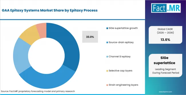
Gaa Epitaxy Systems Market Analysis By Epitaxy Process | Source: Fact.MR
SiGe superlattice growth creates the alternating channel and sacrificial layers that define stacked nanosheets. Thickness, germanium fraction and interface abruptness are repeated many times, making epitaxy a structural device-forming step rather than a simple film deposition. Source-drain epitaxy is also critical for strain and resistance, but the superlattice determines the nanosheet stack itself. (1) Stacked nanosheet formation: a stack of SiGe and Si are epitaxially grown on the Si substrate; the thickness of each layer can be controlled with high precision. (2) Source/drain: n-type or p-type source/drain epitaxial layers are selectively formed on either sides of the exposed nanosheet ends after inner-spacer formation.
Why do Single-wafer reactors lead Reactor Type?
Single-wafer reactors are projected to account for 42.6% share in 2026.
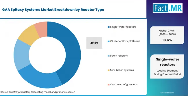
Gaa Epitaxy Systems Market Analysis By Reactor Type | Source: Fact.MR
Single-wafer reactors provide rapid recipe transitions and tight control of temperature, composition and interface timing for complex multilayer stacks. They also isolate a process excursion to one wafer and support cluster integration with pre-clean. Batch systems can improve throughput, but wafer-to-wafer matching and abrupt transitions are harder for demanding GAA sequences. Each architectural step adds buried/stacked epi modules (dielectric wall + stacked n/p sheets), growing epi reactor content per wafer. Buyers therefore tend to treat single-wafer reactors as the practical choice when qualification must balance process capability, repeatability and production economics.
Why does 2 nm class lead Node Application?
2 nm class is projected to account for 41.4% share in 2026.
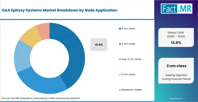
Gaa Epitaxy Systems Market Analysis By Node Application | Source: Fact.MR
The 2 nm class uses GAA nanosheet structures, tighter pitches and thinner process layers, leaving very little room for thickness variation, surface damage or overlay error. Precise measurement is therefore central to channel control, gate formation and interconnect alignment. Older nodes remain important for mature production, but they do not require the same level of process sensitivity or measurement density. Key 2 nm process requirements include uniform nanosheet formation, accurate critical-dimension control, low-defect wafer thinning, tight overlay and stable backside integration.
Why do SiGe alloys lead Material System?
SiGe alloys are projected to account for 44.1% share in 2026.
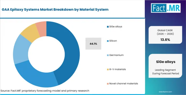
Gaa Epitaxy Systems Market Analysis By Material System | Source: Fact.MR
SiGe alloys provide strain engineering and selective etch contrast between sacrificial and silicon channel layers. Precise germanium composition is therefore central to both device performance and later nanosheet release. Pure silicon remains the channel material in many flows, but it does not provide the same sacrificial-layer selectivity or strain range by itself. GAA module requirements from a toolmaker's IR deck: SiGe/Si: Defect free, Uniform EPI (mold stack); inner spacer dep (low-k, k<5); highly selective SiGe etch for channel release; collapse-free drying; conformal WFM/dipole films. Epitaxy quality is the first-named module in the GAA flow.
Why do Foundries lead End User?
Foundries are projected to account for 31.2% share in 2026.
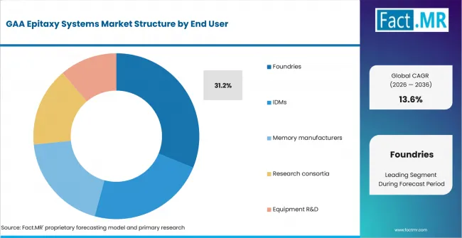
Gaa Epitaxy Systems Market Analysis By End User | Source: Fact.MR
Foundries must offer GAA nodes across multiple customer designs and therefore invest heavily in reactor matching, process windows and yield learning. Epitaxy uniformity becomes part of a platform promise rather than a single internal product recipe. IDMs can co-optimize one architecture more deeply, while foundries need a larger qualified capacity base and broader design tolerance. GlobalFoundries' SG 2015 patent family: delta-layer doping inside embedded stressors to co-optimize strain and resistance (Patsnap patent landscape).
What is accelerating GAA Epitaxy Systems Market adoption, and what is holding it back?
The strongest accelerator is the two epi modules in GAA, while the main restraint is that defects or composition drift in one epitaxial layer propagate through the stacked channel and cannot be repaired later in the flow.
Drivers Impact Analysis
| DRIVER | (~) % IMPACT ON CAGR | GEOGRAPHIC RELEVANCE | IMPACT TIMELINE |
|---|---|---|---|
| The two epi modules in GAA | +3.8% | Global leading-edge fabs | Medium term (2-4 years) |
| Equipment-criticality list (TEL) | +3.1% | Global leading-edge fabs | Medium term (2-4 years) |
| Why SiGe S/D epi matters electrically | +2.6% | Global leading-edge fabs | Medium term (2-4 years) |
| Critical-thickness constraint | +2.0% | Global leading-edge fabs | Medium term (2-4 years) |
Source: Fact.MR analysis. Updated Jul 23, 2026
- The two epi modules in GAA: (1) Stacked nanosheet formation: a stack of SiGe and Si are epitaxially grown on the Si substrate; the thickness of each layer can be controlled with high precision. (2) Source/drain: n-type or p-type source/drain epitaxial layers are selectively formed on either sides of the exposed nanosheet ends after inner-spacer formation.
- Equipment-criticality list (TEL): GAA module requirements from a toolmaker's IR deck: SiGe/Si: Defect free, Uniform EPI (mold stack); inner spacer dep (low-k, k<5); highly selective SiGe etch for channel release; collapse-free drying; conformal WFM/dipole films. Epitaxy quality is the first-named module in the GAA flow.
- Why SiGe S/D epi matters electrically: Selective SiGe growth in recessed S/D cavities induces compressive strain that modifies the valence band, boosting hole mobility (documented gains of 40-100% across MIT/IIT Bombay study data) and drive current in p-type nanosheet FETs; in-situ boron doping at 1-3×10²⁰ cm⁻³ combines strain + conductivity.
- Critical-thickness constraint: SiGe must stay below critical thickness to avoid misfit dislocations and strain relaxation - increasingly hard in nanosheet architectures where S/D volume is limited by inner-spacer dimensions and nanosheet pitch. IBM patents address dislocation-free pseudomorphic growth across the full S/D volume.
Opportunity Impact Analysis
| OPPORTUNITY | (~) % IMPACT ON CAGR | GEOGRAPHIC RELEVANCE | IMPACT TIMELINE |
|---|---|---|---|
| Superlattice discipline | +2.3% | Global leading-edge fabs | Medium term (2-4 years) |
| Delta-layer doping | +1.8% | Global leading-edge fabs | Medium term (2-4 years) |
| Ge-channel extension | +1.4% | Global leading-edge fabs | Medium term (2-4 years) |
Source: Fact.MR analysis. Updated Jul 23, 2026
- Superlattice discipline: Alternating Si/SiGe stacks with angstrom-level thickness repeatability and abrupt interfaces - the channel-release etch selectivity depends directly on epi interface quality (MDPI; TEL).
- Delta-layer doping: GlobalFoundries' SG 2015 patent family: delta-layer doping inside embedded stressors to co-optimize strain and resistance (Patsnap patent landscape).
- Ge-channel extension: KTH (2020) demonstrated selective in-situ-doped SiGe epi on bulk Ge for p+/n junctions - pointing toward Ge/III-V channel GAA successors.
Restraints Impact Analysis
| RESTRAINT | (~) % IMPACT ON CAGR | GEOGRAPHIC RELEVANCE | IMPACT TIMELINE |
|---|---|---|---|
| Primary qualification constraint | -2.0% | Global leading-edge fabs | Medium term (2-4 years) |
| Critical-thickness and dislocation risk | -1.6% | Global leading-edge fabs | Medium term (2-4 years) |
| Export-control and licensing exposure | -1.2% | USA | Short term (<=2 years) |
Source: Fact.MR analysis. Updated Jul 23, 2026
- Primary qualification constraint: Defects or composition drift in one epitaxial layer propagate through the stacked channel and cannot be repaired later in the flow.
- Critical-thickness and dislocation risk: SiGe must stay below critical thickness to avoid misfit dislocations and strain relaxation - increasingly hard in nanosheet architectures where S/D volume is limited by inner-spacer dimensions and nanosheet pitch. IBM patents address dislocation-free pseudomorphic growth across the full S/D volume.
Which countries are scaling GAA Epitaxy Systems Market fastest?
Japan is projected to record a 13.7% CAGR for GAA Epitaxy Systems Market as semiconductor equipment, materials, inspection and memory-process expertise.
- Countries differ less by the headline CAGR than by the type of semiconductor work creating demand for the GAA Epitaxy Systems Market.
- USA demand reflects logic-node development, domestic equipment capability and epitaxy R&D, while Taiwan demand is driven by foundry process ramps, advanced packaging links and local material qualification.
- South Korea pairs memory and logic production with foundry investment, while Japan supplies materials, reactors and process-development expertise.
- Israel develops through advanced logic manufacturing and process-control R&D, while Ireland relies on European logic manufacturing and process-development investment.
- National demand varies with GAA node roadmaps, epitaxy capacity, precursor access, domestic equipment capability and qualification lead times.
Country analysis frames the six profiled markets against North America, Latin America, Europe, East Asia, South Asia & Oceania, and the Middle East & Africa.
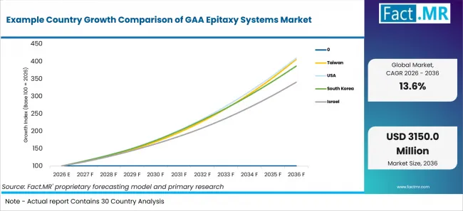
Example Country Growth Comparison Of Gaa Epitaxy Systems Market | Source: Fact.MR
| COUNTRY | CAGR, 2026 to 2036 |
|---|---|
| USA | 15.1% |
| Taiwan | 15.0% |
| South Korea | 14.5% |
| Japan | 13.7% |
| Israel | 13.0% |
| Ireland | 12.6% |
Source: Fact.MR analysis. Updated Jul 23, 2026
What is driving USA's growth through 2036?
15.1% CAGR, supported by leading-edge logic, high-performance computing, federally supported semiconductor R&D and a large domestic equipment base.
Applied Materials brings Centura epitaxy experience and process integration work across GAA epitaxy and inner-spacer formation, while IBM Research Albany contributes nanosheet device research and patent development. Together, these capabilities create a clear qualification pathway for the GAA Epitaxy Systems Market, where semiconductor manufacturers must grow highly uniform Si/SiGe nanosheet stacks and selective source-drain structures with sharp interfaces, tight composition control and very low defect levels at production scale.
What is driving Taiwan's growth through 2036?
15.0% CAGR, shaped by Taiwan's foundry-led process development and epitaxy qualification ecosystem.
Samsung (3 nm GAA/MBCFET first), TSMC (2 nm nanosheet) - the demand side. This environment creates a clear qualification pathway for the GAA Epitaxy Systems Market because buyers must solve the problem of growing highly uniform Si/SiGe nanosheet stacks and selective source-drain structures with abrupt interfaces and minimal defects at production scale.
What is driving South Korea's growth through 2036?
14.5% CAGR, supported by high-volume memory, HBM and vertically integrated semiconductor manufacturing.
Samsung Electronics and SK hynix operate large memory fabrication bases, with strong positions in HBM, advanced DRAM and high-layer NAND. Their vertically integrated structure connects chip design, wafer processing and advanced packaging, which speeds process qualification across new memory generations. This environment creates a clear growth pathway because semiconductor manufacturers must improve uniformity, yield and throughput while handling deeper structures, thinner layers and tighter process limits at production scale.
What is driving Japan's growth through 2036?
13.7% CAGR, underpinned by Japan's equipment, materials and epitaxy-process expertise.
TEL (GAA module portfolio incl. epi-adjacent steps); TEL Miyagi process R&D. This environment creates a clear qualification pathway for the GAA Epitaxy Systems Market because buyers must solve the problem of growing highly uniform Si/SiGe nanosheet stacks and selective source-drain structures with abrupt interfaces and minimal defects at production scale.
What is driving Israel's growth through 2036?
13.0% CAGR, supported by advanced logic manufacturing and process-control R&D.
Israel combines advanced logic-chip manufacturing with strong process-control research. In stacked nanosheet formation, alternating SiGe and silicon layers are grown epitaxially on a silicon substrate, with each layer requiring precise thickness control. This creates a clear commercial need for systems that produce highly uniform Si/SiGe stacks and selective source-drain structures with sharp interfaces, low defect levels, and stable performance as manufacturing capacity and process complexity increase.
What is driving Ireland's growth through 2036?
12.6% CAGR, supported by European logic manufacturing and process-development investment.
Ireland combines European logic manufacturing and process-development investment with a 7.7% share of 2026 demand across the six profiled countries. GAA module requirements from a toolmaker's IR deck: SiGe/Si: Defect free, Uniform EPI (mold stack); inner spacer dep (low-k, k<5); highly selective SiGe etch for channel release; collapse-free drying; conformal WFM/dipole films. The commercial link is the need to solve the problem of growing highly uniform Si/SiGe nanosheet stacks and selective source-drain structures with abrupt interfaces and minimal defects as capacity and process complexity increase.
Who leads the GAA Epitaxy Systems Market?
GAA epitaxy competition centers on reactor architecture, precursor control, in-situ process measurement and the ability to qualify strained or selective epitaxy at advanced nodes.
Applied Materials participates through deposition, etch, materials engineering and integrated process modules. Integrated GAA modules (epi + selective etch + inner spacer). ASM International participates through epitaxy and atomic-layer process equipment. Selective epi for Si/SiGe stacks and S/D; co-optimized with ALD for inner spacers. Tokyo Electron participates through etch, clean, deposition and wafer-bonding process equipment. Published GAA module requirements (defect-free uniform epi first). Lam Research participates through etch, deposition, clean and advanced memory process integration, with relevance determined by its ability to address the challenge of growing highly uniform Si/SiGe nanosheet stacks and selective source-drain structures with abrupt interfaces and minimal defects.
AIXTRON holds a more specialized role through compound-semiconductor and advanced epitaxy systems, particularly where custom integration and service coverage affect qualification. Veeco holds a more specialized role through epitaxy and thin-film process equipment, particularly where custom integration and service coverage affect qualification.
Competition is expected to center on repeatable process performance, integration with adjacent modules, installed-base service and documented capability to address the challenge of growing highly uniform Si/SiGe nanosheet stacks and selective source-drain structures with abrupt interfaces and minimal defects. Buyers are likely to compare accuracy, defect prevention, throughput, recipe stability and the completeness of the delivered process cell.
Which companies are the key providers?
Key companies include Applied Materials; ASM International; Tokyo Electron; Lam Research; AIXTRON; Veeco.
- Applied Materials
- ASM International
- Tokyo Electron
- Lam Research
- AIXTRON
- Veeco
Bibliography
- Applied Materials, Inc. (2025, October 7). Applied Materials unveils next-gen chipmaking products to supercharge AI performance.
- ASM International N.V. (2025). Annual report 2025.
- ASM International N.V. (2025). ASM 3Q25 investor presentation.
- Imec. (2025, November 10–13). ICSI/ISTDM 2025: International Conference on Si Epitaxy and Heterostructures/International Si Technology and Device Meeting.
This Report Addresses
- The report provides strategic intelligence on GAA Epitaxy Systems Market across Epitaxy Process and Reactor Type choices that shape purchasing decisions.
- Segment analysis covers SiGe superlattice growth as the share leader within the 2026 market structure.
- Regional analysis contrasts Taiwan and USA with South Korea and Israel, then evaluates Japan and Ireland through their roles in GAA epitaxy materials, reactors and process development.
- Competitive analysis profiles Applied Materials and ASM International alongside Tokyo Electron and Lam Research, followed by additional active providers.
- Use-case assessment covers the categories and applications that shape demand in the GAA Epitaxy Systems Market across the forecast period.
What does the GAA Epitaxy Systems Market cover?
The market covers equipment and process systems configured to address the challenge of growing highly uniform Si/SiGe nanosheet stacks and selective source-drain structures with abrupt interfaces and minimal defects.
GAA epitaxy systems are selective epitaxial growth (SEG) reactors - reduced-pressure CVD platforms - that grow the Si/SiGe superlattice nanosheet stacks and the raised source/drain (Si:P for nFET, SiGe:B for pFET) of gate-all-around transistors. The segment is defined by defect-free growth on exposed crystal facets, atomic-level thickness control of the sacrificial SiGe vs channel Si layers, and in-situ doping uniformity across 300 mm wafers.
Commercial value includes GAA epitaxy reactors, precursor delivery, temperature and pressure control, wafer handling, in-situ monitoring and service integration. Finished devices, packaging value and unrelated wafer-fab equipment are excluded.
What is included in the scope?
The scope includes systems used by foundries and the other end-user groups listed in the segmentation.
The market is segmented by Epitaxy Process, including SiGe superlattice growth, Source-drain epitaxy, Channel Si epitaxy, Selective cap layers, Strain engineering layers; Reactor Type, including Single-wafer reactors, Cluster epitaxy platforms, Batch reactors, Mini-batch systems, Custom configurations; Node Application, including 2 nm class, 3 nm class, Sub-2 nm class, 5 nm class, Research nodes; Material System, including SiGe alloys, Silicon, Germanium, III-V materials, Novel channel materials; End User, including Foundries, IDMs, Memory manufacturers, Research consortia, Equipment R&D.
Precursor conditioning, gas delivery, wafer transfer, in-situ metrology and reactor-control modules are included only when delivered with the configured epitaxy platform.
What is excluded from the scope?
The scope excludes unrelated semiconductor equipment, standalone materials and components sold independently of the configured system.
It also excludes facility construction, cleanroom infrastructure, the value of processed wafers or packages, and adjacent process steps that are not part of the defined equipment category.
How Was the Analysis Built?
Fact.MR is of the opinion that this assessment combines structured market analysis with a review of public information and industry evidence relevant to the market.
- Market Assessment: The analysis considers demand patterns, supply conditions, segment mix, country activity, company participation, and adoption trends.
- Evidence Review: Public company disclosures, government and regulatory publications, trade information, technical literature, and industry records inform the assessment.
- Validation and Updates: Findings are cross-checked against available market indicators and reviewed when material market developments emerge.
Segmentation
What is the report's scope and coverage?
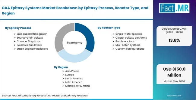
Gaa Epitaxy Systems Market Breakdown By Epitaxy Process, Reactor Type, And Region | Source: Fact.MR
| Attribute | Details |
|---|---|
| Quantitative Units | USD 880.0 million in 2026 to USD 3,150.0 million by 2036 at a 13.6% CAGR |
| Market Definition | GAA epitaxy systems are selective epitaxial growth (SEG) reactors - reduced-pressure CVD platforms - that grow the Si/SiGe superlattice nanosheet stacks and the raised source/drain (Si:P for nFET, SiGe:B for pFET) of gate-all-around transistors. The segment is defined by defect-free growth on exposed crystal facets, atomic-level thickness control of the sacrificial SiGe vs channel Si layers, and in-situ doping uniformity across 300 mm wafers. |
| Epitaxy Process | SiGe superlattice growth; Source-drain epitaxy; Channel Si epitaxy; Selective cap layers; Strain engineering layers |
| Reactor Type | Single-wafer reactors; Cluster epitaxy platforms; Batch reactors; Mini-batch systems; Custom configurations |
| Node Application | 2 nm class; 3 nm class; Sub-2 nm class; 5 nm class; Research nodes |
| Material System | SiGe alloys; Silicon; Germanium; III-V materials; Novel channel materials |
| End User | Foundries; IDMs; Memory manufacturers; Research consortia; Equipment R&D |
| Regions Covered | North America; Latin America; Europe; East Asia; South Asia & Oceania; Middle East & Africa |
| Countries Covered | Taiwan; USA; South Korea; Israel; Japan; Ireland |
| Key Companies Profiled | Applied Materials; ASM International; Tokyo Electron; Lam Research; AIXTRON; Veeco |
| Forecast Period | 2026 to 2036 |
| Approach | Hybrid top-down and bottom-up approach using demand indicators across Epitaxy Process; Reactor Type; Node Application; Material System; End User; country-level growth; company participation and adoption trends |
Source: Fact.MR analysis. Updated Jul 23, 2026
How is the market segmented?
-
By Epitaxy Process:
- SiGe superlattice growth
- Source-drain epitaxy
- Channel Si epitaxy
- Selective cap layers
- Strain engineering layers
-
By Reactor Type:
- Single-wafer reactors
- Cluster epitaxy platforms
- Batch reactors
- Mini-batch systems
- Custom configurations
-
By Node Application:
- 2 nm class
- 3 nm class
- Sub-2 nm class
- 5 nm class
- Research nodes
-
By Material System:
- SiGe alloys
- Silicon
- Germanium
- III-V materials
- Novel channel materials
-
By End User:
- Foundries
- IDMs
- Memory manufacturers
- Research consortia
- Equipment R&D
-
By Region:
- North America
- Latin America
- Europe
- East Asia
- South Asia & Oceania
- Middle East & Africa
Frequently Asked Questions
Which Epitaxy Process leads the GAA Epitaxy Systems Market?
Which Reactor Type leads the GAA Epitaxy Systems Market?
Which Node Application leads the GAA Epitaxy Systems Market?
Which Material System leads the GAA Epitaxy Systems Market?
Which End User leads the GAA Epitaxy Systems Market?
What CAGR is projected for USA in the GAA Epitaxy Systems Market?
What CAGR is projected for Taiwan in the GAA Epitaxy Systems Market?
What CAGR is projected for South Korea in the GAA Epitaxy Systems Market?
What CAGR is projected for Japan in the GAA Epitaxy Systems Market?
What CAGR is projected for Israel in the GAA Epitaxy Systems Market?
What CAGR is projected for Ireland in the GAA Epitaxy Systems Market?
What is the primary driver of the GAA Epitaxy Systems Market?
What is the main restraint in the GAA Epitaxy Systems Market?
Who worked on this report


Preview the report firsthand - request a free sample
Free SampleGet the brochure for pricing and purchase details
Download PDF