- Market Value (2025): USD 163.8 Mn
- Estimated Value (2026): USD 192.0 Mn
- Forecast Value (2036): USD 940.0 Mn
- CAGR (2026-2036): 17.2%
What is the Glass Substrate Metallizers Market forecast to be worth by 2036?
USD 192.0 million in 2026 to USD 940.0 million by 2036, at a 17.2% CAGR.
- The Glass Substrate Metallizers Market crossed a valuation of USD 163.8 million in 2025, supported by demand from Substrate manufacturers serving TGV sidewall metallization workflows that require creating adherent, conformal and void-free conductive paths through glass vias and across large, dimensionally stable panels.
- Demand is projected to increase from USD 192.0 million in 2026 to USD 940.0 million by 2036.
- The market is forecast to record a 17.2% CAGR from 2026 to 2036 as tgv metallization stack (production practice), void and interface-defect control and full flow remain central purchase reasons.
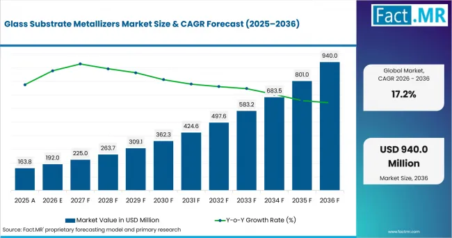
Glass Substrate Metallizers Market Value Analysis | Source: Fact.MR
What are the defining numbers behind Glass Substrate Metallizers Market growth?
USD 748.0 million absolute opportunity is expected by 2036.
- Demand Drivers in the Market
- TGV metallization stack (production practice): Equipment demand is converging on a standard production stack - PVD titanium/copper seed (roughly 30/300 nm) for adhesion and initial conductivity, followed by conformal copper electroplate, with fill strategy set by via size: full superfill below 50 micrometers, conformal coat plus cap plating from 50-100 micrometers, and conformal coat plus paste fill plus cap above 100 micrometers - giving buyers a defined process to specify tools against. [2]
- Void and interface-defect control: Demand for adhesion-focused metallization equipment is driven by a problem organic substrates simply don't have: glass's smoothness inhibits the mechanical anchoring that keeps metal attached, making adhesion-layer and seed-coverage quality a first-order purchase criterion rather than a secondary spec.
- Full flow: Buyers are qualifying full multi-step metallization lines rather than single tools, running pre-clean, adhesion-layer dip coat and sinter, palladium activation, roughly 400 nm electroless copper, anneal, dry-film lithography, 15-20 micrometer electrolytic copper, strip and anneal, then differential etch - a long, tightly sequenced flow that favors vendors who can deliver more of it as an integrated line. [3]
- PVD lineage for deep features: Demand for advanced sputtering architectures is rising as via aspect ratios deepen: PVD for via/barrier/seed coverage has evolved from diode to long-throw to collimated to ionized-metal plasma to self-ionized plasma sputtering, and measured tantalum step coverage on 10x60 micrometer vias ranges from 8.6% to 23.5% at bottom corners depending on power settings - directly shaping which PVD architecture a glass-via line needs. [4]
- Key Segments Analyzed
- By Metallization Method: PVD sputtering is projected to hold 33.0% share in 2026, supported by a clear process advantage: PVD sputtering establishes the adhesion, barrier and seed layers needed to initiate reliable plating on an electrically insulating glass surface. It gives precise film control over the panel face and via entrances.
- By Metal System: Copper is projected to hold 44.5% share in 2026, supported by a clear process advantage: Copper combines low electrical resistance with a mature plating, patterning and redistribution infrastructure. It therefore provides the most practical route from glass vias to high-density package wiring.
- By Feature Type: TGV sidewall metallization is projected to hold 42.8% share in 2026, supported by a clear process advantage: TGV sidewall metallization is the critical continuity step: a discontinuity anywhere along the glass via becomes an open after fill or redistribution. Conformality and adhesion inside the via are harder than coating the planar panel surface.
- By Substrate Format: Panel format is projected to hold 47.6% share in 2026, supported by a clear process advantage: Panel processing spreads equipment and material cost across a larger area and matches the economic promise of glass cores. It also requires exceptional uniformity because thickness, stress and plating current vary across a wide field.
- By End User: Substrate manufacturers are projected to hold 28.9% share in 2026, supported by a clear process advantage: Substrate manufacturers integrate seed deposition, plating, patterning and reliability qualification and therefore capture the direct value of metallization yield. They can also co-optimize the via geometry and metal stack.
- Analyst Opinion at Fact.MR
- Shambhu Nath Jha, Sr. Consultant at Fact.MR, states, 'Buyers should evaluate the complete process sequence around creating adherent, conformal and void-free conductive paths through glass vias and across large, dimensionally stable panels. Technical review should focus on repeatability, integration, defect control and production throughput rather than a single headline specification. Suppliers that connect tool performance to measurable yield and qualification results are likely to build trust faster.'
- Strategic Implications
- Evaluation should couple adhesion, via-fill morphology, panel uniformity and thermal-cycle reliability rather than treating sputter and plating as separate purchases.
- Equipment suppliers should document how their systems address the challenge of creating adherent, conformal and void-free conductive paths through glass vias and across large, dimensionally stable panels across production-representative wafers, panels, dies or packages.
- Procurement teams should compare metallization adhesion, via and trace coverage, copper-stack reliability, panel uniformity, seed-layer control and compatibility with glass-core packaging processes.
Japan is projected to record a 17.7% CAGR; South Korea, 18.0%; Taiwan, 18.4%; Austria, 16.5%; and USA, 18.5% from 2026 to 2036. These country CAGRs are aggregate forecasts. Local semiconductor equipment, materials, memory, foundry, packaging and R&D activity shape demand conditions but do not independently produce the forecast rates.
How does the Glass Substrate Metallizers Market break down by segment?
PVD sputtering leads Metallization Method with a 33.0% share, while Copper accounts for 44.5% of Metal System in 2026.
Why does PVD sputtering lead Metallization Method?
PVD sputtering is projected to account for 33.0% share in 2026.
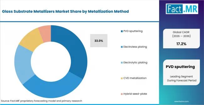
Glass Substrate Metallizers Market Analysis By Metallization Method | Source: Fact.MR
PVD sputtering establishes the adhesion, barrier and seed layers needed to initiate reliable plating on an electrically insulating glass surface. It gives precise film control over the panel face and via entrances. Electroless plating can improve coverage in recessed structures, but bath stability, selectivity and adhesion control add chemical complexity. PVD Ti/Cu seed (30/300 nm) for adhesion + initial conductivity, then conformal Cu electroplate; fill strategy by via size - <50 µm: full superfilling; 50-100 µm: conformal coat + cap plating; >100 µm: conformal coat + paste fill + cap. [2] Buyers therefore tend to treat PVD sputtering as the practical choice when qualification must balance process capability, repeatability and production economics.
Why does Copper lead Metal System?
Copper is projected to account for 44.5% share in 2026.
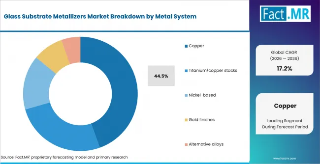
Glass Substrate Metallizers Market Analysis By Metal System | Source: Fact.MR
Copper combines low electrical resistance with a mature plating, patterning and redistribution infrastructure. It therefore provides the most practical route from glass vias to high-density package wiring. Titanium-copper stacks improve adhesion and barrier performance, but copper remains the primary current-carrying material and the largest equipment workload. Unlike an organic substrate it is challenging to metalize a glass surface because the smoothness of glass inhibits mechanical anchoring. Documented solution: a dip-coated metal-oxide adhesion-promotion layer (sol-gel, conformal inside TGVs) enabling electroless Cu directly on glass, then electrolytic build-up (SAP flow), with annealing for adhesion; the metal-oxide layer is differentially etchable, avoiding a separate Ti/Cr etch step. Buyers therefore tend to treat copper as the practical choice when qualification must balance process capability, repeatability and production economics.
Why does TGV sidewall metallization lead Feature Type?
TGV sidewall metallization is projected to account for 42.8% share in 2026.
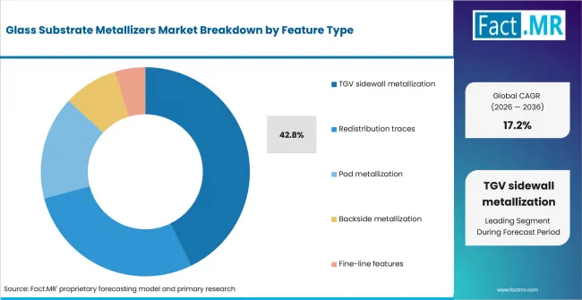
Glass Substrate Metallizers Market Analysis By Feature Type | Source: Fact.MR
TGV sidewall metallization is the critical continuity step: a discontinuity anywhere along the glass via becomes an open after fill or redistribution. Conformality and adhesion inside the via are harder than coating the planar panel surface. Redistribution traces are also important, but they depend on a reliable through-glass connection already being established. Displacing PVD seed for TGV sidewalls (conformality on high-AR glass vias), enabled by metal-oxide adhesion layers (Atotech/MKS VitroCoat-line chemistry documented in IMAPS paper). Buyers therefore tend to treat TGV sidewall metallization as the practical choice when qualification must balance process capability, repeatability and production economics.
Why does Panel format lead Substrate Format?
Panel format is projected to account for 47.6% share in 2026.
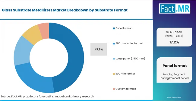
Glass Substrate Metallizers Market Analysis By Substrate Format | Source: Fact.MR
Panel processing spreads equipment and material cost across a larger area and matches the economic promise of glass cores. It also requires exceptional uniformity because thickness, stress and plating current vary across a wide field. A 300 millimeter wafer format is easier to integrate with semiconductor tools, but it gives up part of the panel-level cost advantage. For via/barrier/seed coverage, sputtering evolved from diode to long-throw to collimated to ionized-metal plasma (IMP) to self-ionized plasma (SIP, tens of kW DC); measured Ta step coverage on 10×60 µm vias ranges 8.6-23.5% at bottom corners depending on DC/substrate power - the physics glass-via metallizers inherit. [4] Buyers therefore tend to treat panel format as the practical choice when qualification must balance process capability, repeatability and production economics.
Why do Substrate manufacturers lead End User?
Substrate manufacturers are projected to account for 28.9% share in 2026.
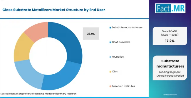
Glass Substrate Metallizers Market Analysis By End User | Source: Fact.MR
Substrate manufacturers integrate seed deposition, plating, patterning and reliability qualification and therefore capture the direct value of metallization yield. They can also co-optimize the via geometry and metal stack. OSATs specify electrical and package requirements, but the metallization toolset sits primarily in the substrate fabrication flow. IEEE EPS/AGC chapter reports fully Cu-filled TGVs maintaining stable electrical characteristics through rigorous thermal cycling, with SeWaRe (stress-warping-reliability) mitigations via substrate design. [5] Buyers therefore tend to treat substrate manufacturers as the practical choice when qualification must balance process capability, repeatability and production economics.
What is accelerating Glass Substrate Metallizers Market adoption, and what is holding it back?
The strongest accelerator is TGV metallization stack (production practice), while the main restraint is that discontinuous seed layers, trapped gas, stress and poor adhesion create latent opens that may appear only after thermal cycling.
Drivers Impact Analysis
| DRIVER | MARKET RELEVANCE | PRIMARY ADOPTION CONTEXT | RELEVANCE HORIZON |
|---|---|---|---|
| TGV metallization stack (production practice) | High | Global leading-edge fabs | 2026 to 2036 |
| Void and interface-defect control | High | Global leading-edge fabs | 2026 to 2036 |
| Full flow | High | Global leading-edge fabs | 2026 to 2036 |
| PVD lineage for deep features | High | Global leading-edge fabs | 2026 to 2036 |
- TGV metallization stack (production practice): PVD Ti/Cu seed (30/300 nm) for adhesion + initial conductivity, then conformal Cu electroplate; fill strategy by via size - <50 µm: full superfilling; 50-100 µm: conformal coat + cap plating; >100 µm: conformal coat + paste fill + cap. [2]
- Void and interface-defect control: Unlike an organic substrate it is challenging to metalize a glass surface because the smoothness of glass inhibits mechanical anchoring.
- Full flow: Pre-clean to adhesion-layer dip coat + sinter to Pd activation to ~400 nm electroless Cu + anneal to dry-film litho to 15-20 µm electrolytic Cu to strip + anneal to differential etch. [3]
- PVD lineage for deep features: For via/barrier/seed coverage, sputtering evolved from diode to long-throw to collimated to ionized-metal plasma (IMP) to self-ionized plasma (SIP, tens of kW DC); measured Ta step coverage on 10×60 µm vias ranges 8.6High at bottom corners depending on DC/substrate power - the physics glass-via metallizers inherit. [4]
Opportunity Impact Analysis
| OPPORTUNITY | MARKET RELEVANCE | PRIMARY ADOPTION CONTEXT | RELEVANCE HORIZON |
|---|---|---|---|
| Electroless-first metallization | High | Global leading-edge fabs | 2026 to 2036 |
| Superfilling chemistry for <50 µm vias | High | Global leading-edge fabs | 2026 to 2036 |
| Panel plating tools | High | South Korea | Short term (<=2 years) |
- Electroless-first metallization: Displacing PVD seed for TGV sidewalls (conformality on high-AR glass vias), enabled by metal-oxide adhesion layers (Atotech/MKS VitroCoat-line chemistry documented in IMAPS paper).
- Superfilling chemistry for <50 µm vias: Organic additive packages (suppressor/accelerator/leveler) tuned for glass vias; full-fill demonstrated reliable under thermal cycling (IEEE/AGC).
- Panel plating tools: (Vertical/horizontal conveyorized, 510×515 mm and 600×600 mm) being qualified as TSMC CoPoS (mid-2026 pilot) and Korean/Intel programs ramp. [6]
Restraints Impact Analysis
| RESTRAINT | MARKET RELEVANCE | PRIMARY ADOPTION CONTEXT | RELEVANCE HORIZON |
|---|---|---|---|
| Primary qualification constraint | High | Global leading-edge fabs | 2026 to 2036 |
| Surface-state degradation | High | Global leading-edge fabs | 2026 to 2036 |
| Alignment and registration risk | High | Global leading-edge fabs | 2026 to 2036 |
- Primary qualification constraint: Discontinuous seed layers, trapped gas, stress and poor adhesion create latent opens that may appear only after thermal cycling.
- Surface-state degradation: Documented solution: a dip-coated metal-oxide adhesion-promotion layer (sol-gel, conformal inside TGVs) enabling electroless Cu directly on glass, then electrolytic build-up (SAP flow), with annealing for adhesion; the metal-oxide layer is differentially etchable, avoiding a separate Ti/Cr etch step.
- Alignment and registration risk: Registration and glass-chemistry compatibility (wet etch attack) are named equipment constraints. [2]
Which countries are scaling Glass Substrate Metallizers Market fastest?
In USA, Glass Substrate Metallizers Market is projected to advance at 18.5% CAGR from 2026 to 2036. Local leading-edge logic, high-performance computing, federally supported semiconductor R&D and a large domestic equipment base.
- Countries differ less by the headline CAGR than by the type of semiconductor work creating demand for the Glass Substrate Metallizers Market.
- China follows a pathway shaped by rapid domestic capacity build-out, local-equipment substitution and tighter access to controlled foreign tools. USA takes a different path through leading-edge logic, high-performance computing, federally supported semiconductor R&D and a large domestic equipment base.
- Taiwan and South Korea remain aligned through distinct combinations of device production, equipment development and advanced packaging investment.
- Japan develops through semiconductor equipment, materials, inspection and memory-process expertise, while Austria relies on European wafer-bonding and substrate-equipment expertise, including a strong advanced-packaging supplier base.
- Country forecasts aggregate demand across fab investment, packaging programs, local equipment capability, trade conditions and qualification timing; these conditions inform rather than independently determine the modeled rates.
Country analysis covers the six profiled markets in the context of North America, Latin America, Europe, East Asia, South Asia & Oceania, and the Middle East & Africa.
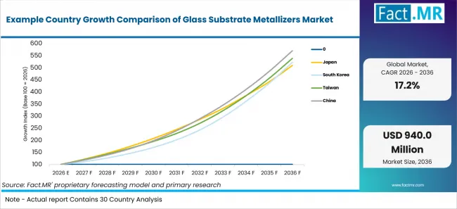
Example Country Growth Comparison Of Glass Substrate Metallizers Market | Source: Fact.MR
| COUNTRY | CAGR, 2026 to 2036 |
|---|---|
| USA | 18.5% |
| Taiwan | 18.4% |
| South Korea | 18.0% |
| Japan | 17.7% |
| Austria | 16.5% |
What is driving USA's growth through 2036?
18.5% CAGR from 2026 to 2036. Local leading-edge logic, high-performance computing, federally supported semiconductor R&D and a large domestic equipment base.
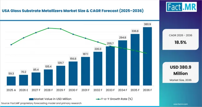
Glass Substrate Metallizers Market Country Value Analysis | Source: Fact.MR
The Arizona research line, Absolics' Covington activity and Georgia Tech's adhesion-layer research give U.S. programs a route to test glass-via metallization and qualification before larger production deployment.
What is driving Taiwan's growth through 2036?
18.4% CAGR from 2026 to 2036. Local leading foundry production, advanced packaging and a dense OSAT and substrate supply chain.
Taiwan's CoPoS activity and the participation of Unimicron and Kinsus position the market around panel metallization, supplier qualification and OSAT integration.
What is driving South Korea's growth through 2036?
18.0% CAGR from 2026 to 2036. Local high-volume memory, HBM and vertically integrated semiconductor manufacturing.
What is driving Japan's growth through 2036?
17.7% CAGR from 2026 to 2036. Local semiconductor equipment, materials, inspection and memory-process expertise.
Japan's glass, plating-chemistry and equipment suppliers support a materials-and-tool ecosystem for panel metallization, with qualification focused on adhesion and via-wall coverage.
What is driving Austria's growth through 2036?
16.5% CAGR from 2026 to 2036. Local European wafer-bonding and substrate-equipment expertise, including a strong advanced-packaging supplier base.
Austria combines European wafer-bonding and substrate-equipment expertise, including a strong advanced-packaging supplier base with a 11.6% share of 2026 demand across the six profiled countries. Unlike an organic substrate it is challenging to metalize a glass surface because the smoothness of glass inhibits mechanical anchoring. The commercial link is the need to solve the problem of creating adherent, conformal and void-free conductive paths through glass vias and across large, dimensionally stable panels as capacity and process complexity increase.
Who leads the Glass Substrate Metallizers Market?
Applied Materials and Atotech (MKS) lead the competitive landscape, followed by Lam Research and Evatec as the next tier of challengers.
Applied Materials participates through deposition, etch, materials engineering and integrated process modules. SIP/IMP PVD heritage; investor in Absolics (JV with SKC). Atotech (MKS) participates through wet metallization and plating chemistry or equipment. Documented glass adhesion promoter + electroless + electrolytic chemistry set (VitroCoat/SigmaTech/CupraTech/Cupracid products cited in IMAPS work). Lam Research participates through etch, deposition, clean and advanced memory process integration, with relevance determined by its ability to address the challenge of creating adherent, conformal and void-free conductive paths through glass vias and across large, dimensionally stable panels. Evatec participates through thin-film deposition and metallization equipment, with relevance determined by its ability to address the challenge of creating adherent, conformal and void-free conductive paths through glass vias and across large, dimensionally stable panels.
Semsysco holds a more specialized role through semiconductor wet-process and metallization systems, particularly where custom integration and service coverage affect qualification. Ulvac holds a more specialized role through vacuum deposition and thin-film equipment, particularly where custom integration and service coverage affect qualification.
Competition is expected to center on repeatable process performance, integration with adjacent modules, installed-base service and documented capability to address the challenge of creating adherent, conformal and void-free conductive paths through glass vias and across large, dimensionally stable panels. Buyers are likely to compare accuracy, defect prevention, throughput, recipe stability and the completeness of the delivered process cell.
Which companies are the key providers?
Key companies include Applied Materials; Atotech (MKS); Lam Research; Evatec; Semsysco; Ulvac.
- Applied Materials
- Atotech (MKS)
- Lam Research
- Evatec
- Semsysco
- Ulvac
Bibliography
- [1] IMAPS. (n.d.). 55855 Using A Metal Oxide Adhesion Layer And Wet Chemical Cu Metallization For Fine Line Pattern Formation On Glass.
- [2] Imapsjmep. (n.d.). 103753.
- [3] Eps. (n.d.). Glass Substrates Adv Substrates Tc Updated Nov25.
- [4] Photoncap. (n.d.). Investment Map 15 Companies In The.
- [5] Koreaherald. (n.d.). Source document.
This Report Addresses
- The report provides strategic intelligence on Glass Substrate Metallizers Market across Metallization Method and Metal System choices that shape purchasing decisions.
- Segment analysis covers PVD sputtering as the share leader within the 2026 market structure.
- Regional outlook evaluates Japan and South Korea alongside Taiwan, while Austria and USA complete the growth comparison.
- Competitive analysis profiles Applied Materials and Atotech (MKS) alongside Lam Research and Evatec, followed by additional active providers.
- Use-case assessment covers the categories and applications that shape demand in the Glass Substrate Metallizers Market across the forecast period.
What does the Glass Substrate Metallizers Market cover?
The market covers equipment and process systems configured to address the challenge of creating adherent, conformal and void-free conductive paths through glass vias and across large, dimensionally stable panels.
Glass substrate metallizers are the PVD (barrier/seed sputtering), electroless plating, electrolytic plating, and adhesion-promotion systems that put copper on and through glass: RDL on ultra-smooth glass faces plus conformal or filled metallization of TGV sidewalls. The segment is defined by the adhesion problem - glass is too smooth for mechanical anchoring, unlike organic substrates.
Commercial value includes PVD sputtering, electroless and electrolytic plating, adhesion promotion, panel handling, inspection, process-control software and integration support. Finished semiconductor devices, package value and unrelated parent-market equipment are excluded.
What is included in the scope?
The scope includes systems used by substrate manufacturers and the other end-user groups listed in the segmentation.
The market is segmented by Metallization Method, including PVD sputtering, Electroless plating, Electrolytic plating, CVD metallization, Hybrid seed-plate; Metal System, including Copper, Titanium/copper stacks, Nickel-based, Gold finishes, Alternative alloys; Feature Type, including TGV sidewall metallization, Redistribution traces, Pad metallization, Backside metallization, Fine-line features; Substrate Format, including Panel format, 300 mm wafer format, Large panel (>500 mm), 200 mm format, Custom formats; End User, including Substrate manufacturers, OSAT providers, Foundries, IDMs, Research institutes.
Panel handling, cleaning, activation, metrology, process-control and support modules are included when supplied as part of a glass-substrate metallization system.
What is excluded from the scope?
The scope excludes unrelated semiconductor equipment, standalone materials and components sold independently of the configured system.
It also excludes facility construction, cleanroom infrastructure, the value of processed wafers or packages, and adjacent process steps that are not part of the defined equipment category.
How Was the Analysis Built?
Fact.MR is of the opinion that this assessment combines structured market analysis with a review of public information and industry evidence relevant to the market.
- Market Assessment: The analysis considers demand patterns, supply conditions, segment mix, country activity, company participation, and adoption trends.
- Evidence Review: Public company disclosures, government and regulatory publications, trade information, technical literature, and industry records inform the assessment.
- Validation and Updates: Findings are cross-checked against available market indicators and reviewed when material market developments emerge.
What is the report's scope and coverage?
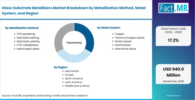
Glass Substrate Metallizers Market Breakdown By Metallization Method, Metal System, And Region | Source: Fact.MR
| Attribute | Details |
|---|---|
| Quantitative Units | USD 192.0 million in 2026 to USD 940.0 million by 2036 at 17.2% CAGR |
| Market Definition | Glass substrate metallizers are the PVD (barrier/seed sputtering), electroless plating, electrolytic plating, and adhesion-promotion systems that put copper on and through glass: RDL on ultra-smooth glass faces plus conformal or filled metallization of TGV sidewalls. The segment is defined by the adhesion problem - glass is too smooth for mechanical anchoring, unlike organic substrates. |
| Metallization Method | PVD sputtering; Electroless plating; Electrolytic plating; CVD metallization; Hybrid seed-plate |
| Metal System | Copper; Titanium/copper stacks; Nickel-based; Gold finishes; Alternative alloys |
| Feature Type | TGV sidewall metallization; Redistribution traces; Pad metallization; Backside metallization; Fine-line features |
| Substrate Format | Panel format; 300 mm wafer format; Large panel (>500 mm); 200 mm format; Custom formats |
| End User | Substrate manufacturers; OSAT providers; Foundries; IDMs; Research institutes |
| Regions Covered | North America; Latin America; Europe; East Asia; South Asia & Oceania; Middle East & Africa |
| Countries Covered | Japan; South Korea; Taiwan; Austria; USA |
| Key Companies Profiled | Applied Materials; Atotech (MKS); Lam Research; Evatec; Semsysco; Ulvac |
| Forecast Period | 2026 to 2036 |
| Approach | Hybrid top-down and bottom-up approach using demand indicators across Metallization Method; Metal System; Feature Type; Substrate Format; End User; country-level growth; company participation and adoption trends |
How is the market segmented?
-
By Metallization Method:
- PVD sputtering
- Electroless plating
- Electrolytic plating
- CVD metallization
- Hybrid seed-plate
-
By Metal System:
- Copper
- Titanium/copper stacks
- Nickel-based
- Gold finishes
- Alternative alloys
-
By Feature Type:
- TGV sidewall metallization
- Redistribution traces
- Pad metallization
- Backside metallization
- Fine-line features
-
By Substrate Format:
- Panel format
- 300 mm wafer format
- Large panel (>500 mm)
- 200 mm format
- Custom formats
-
By End User:
- Substrate manufacturers
- OSAT providers
- Foundries
- IDMs
- Research institutes
-
By Region:
- North America
- Latin America
- Europe
- South Asia & Oceania
- Middle East & Africa