- Market Value (2025): USD 1.5 Bn
- Estimated Value (2026): USD 1.6 Bn
- Forecast Value (2036): USD 3.2 Bn
- CAGR (2026-2036): 7.2%
What is the Bare Die Shipping & Handling and Processing & Storage Market forecast to be worth by 2036?
USD 3.2 billion by 2036.
- The Bare Die Shipping & Handling and Processing & Storage Market reached USD 1.5 billion in 2025.
- Demand is projected to increase from USD 1.6 billion in 2026 to USD 3.2 billion by 2036.
- The market is forecast to record a 7.2% CAGR from 2026 to 2036.
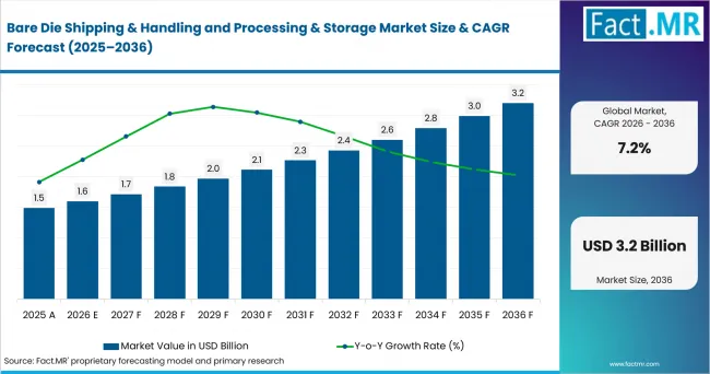
Bare Die Shipping & Handling And Processing & Storage Market Value Analysis | Source: Fact.MR
What are the defining numbers behind Bare Die Shipping & Handling and Processing & Storage Market growth?
An absolute opportunity of USD 1.6 billion is expected between 2026 and 2036.
- Demand Drivers in the Market
- Expansion of semiconductor assembly and advanced packaging is increasing the number of die-level transfer steps requiring protective handling. SEMI projects assembly and packaging equipment sales to rise 9.6% to USD 6.7 billion in 2026 after increasing 20.8% in 2025. Advanced and heterogeneous packaging adds more die placement, inspection and interconnection stages, creating demand for carriers that protect exposed die between processes.
- AI and high-bandwidth-memory architectures are increasing the use of multi-die configurations. SEMI links current back-end equipment expansion to more complex device architectures and heterogeneous packaging. More dies within one package increase the number of pick-and-place movements before final encapsulation, raising the operational value of precise handling and intermediate storage.
- Electrostatic discharge remains a direct risk during bare die handling. The EOS/ESD Association states that ESD can alter semiconductor electrical characteristics and can degrade or destroy a device. Its ANSI/ESD S541 standard defines protective packaging requirements for ESD-sensitive items throughout production, transport and storage. This creates demand for static-dissipative trays, shielding materials and controlled handling procedures.
- Contamination control is becoming more demanding as semiconductor dimensions shrink. The EOS/ESD Association notes that charged surfaces can attract airborne particles and that contamination reaching semiconductor circuitry can cause defects and reduce yield. Bare die remains exposed until packaging, making clean storage and low-contact transport relevant across inspection and assembly operations.
- Semiconductor capacity additions increase the physical volume of wafers and dies moving through production. SEMI projected foundry capacity to reach 12.7 million wafers per month by 2026, while new investment continues across advanced logic and memory. Higher wafer throughput translates into more singulated die requiring controlled handling before packaging or integration.
- Key Segments Analyzed
- Bare Die Handling Systems account for 68.4% of Product in 2026, supported by the need for controlled pickup and transfer of exposed die before packaging.
- Semiconductor Manufacturing holds 41.9% of Application in 2026 as die move through inspection and testing before assembly.
- Semiconductor Foundries account for 77.2% of End Use in 2026, supported by high wafer throughput and growing advanced packaging activity.
- Automated Die Handling Technology represents 57.3% of Technology in 2026 because automated transfer improves precision and repeatability at production scale.
- Integrated Handling Platforms hold 63.8% of Formulation in 2026 as manufacturers combine handling hardware with control systems for die movement and traceability.
- Direct Semiconductor Sales account for 45.6% of Distribution Channel in 2026 because carrier specifications and automation interfaces often require direct technical qualification.
- Analyst Opinion at Fact.MR
- Shambhu Nath Jha, Senior Consultant at Fact.MR, states, “Bare die is handled before the protection provided by a conventional semiconductor package, so each movement creates potential exposure to electrostatic discharge and physical damage. Demand will increasingly favour systems that combine secure die retention with automation compatibility and controlled storage as advanced packaging places more dies within complex assemblies.”
- Strategic Implications
- Suppliers should design handling products around die dimensions, fragility and ESD sensitivity rather than offer one carrier specification across semiconductor applications.
- Automation compatibility will become more important as packaging lines increase throughput. Trays and shipping configurations that work with robotic transfer can reduce manual intervention between process steps.
- Semiconductor customers are likely to give greater weight to traceability. Linking die identity with handling and storage records can support process control when several dies are combined within one package.
- Local supply near semiconductor manufacturing and packaging clusters can reduce replenishment risk for trays, shielding materials and other handling consumables used continuously in production.
How does the Bare Die Shipping & Handling and Processing & Storage Market break down by segment?
The market is segmented by Product, Application, End Use, Technology, Formulation and Distribution Channel.
Why do Bare Die Handling Systems lead Product?
Bare Die Handling Systems are projected to account for a 68.4% share in 2026.
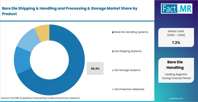
Bare Die Shipping & Handling And Processing & Storage Market Analysis By Product | Source: Fact.MR
Bare die handling systems lead because the die remains mechanically exposed after singulation and before final packaging. Direct contact with active surfaces or edges can damage a component, while uncontrolled movement can affect orientation before inspection or assembly.
Handling systems therefore use controlled pickup and retention methods that allow dies to move between equipment without unnecessary contact. Vacuum pick-and-place systems are suitable where individual dies must be transferred repeatedly, while mechanical systems serve applications requiring stable positioning.
Commercial products illustrate the operating requirement. Entegris offers reusable polymer trays intended to protect bare die during shipping and storage while remaining compatible with manual and automated tool handling. This combination of protection and equipment compatibility supports the segment’s role across semiconductor production.
Why does Semiconductor Manufacturing lead Application?
Semiconductor Manufacturing is projected to account for a 41.9% share in 2026.
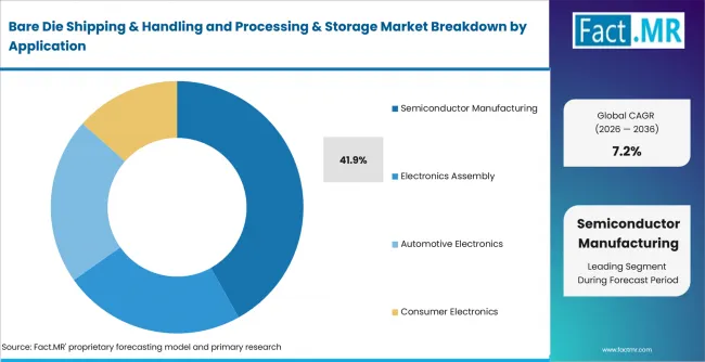
Bare Die Shipping & Handling And Processing & Storage Market Analysis By Application | Source: Fact.MR
Semiconductor manufacturing leads because bare die handling occurs at several points between wafer completion and packaged-device output. Dies may need to move through visual inspection, electrical testing or temporary storage before die attach and subsequent packaging.
Advanced packaging increases the number of these movements. Chiplet and heterogeneous-integration architectures place several semiconductor dies into one package, making accurate handling important for assembly yield.
SEMI projects assembly and packaging equipment sales to reach USD 6.7 billion in 2026, with continued expansion associated with advanced packaging and increasingly complex semiconductor architectures. More packaging activity increases demand for systems that preserve die condition during intermediate processing.
Why do Semiconductor Foundries lead End Use?
Semiconductor Foundries are projected to account for a 77.2% share in 2026.
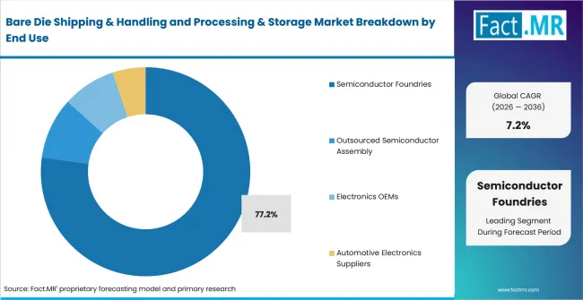
Bare Die Shipping & Handling And Processing & Storage Market Analysis By End Use | Source: Fact.MR
Semiconductor foundries lead because high wafer output creates substantial downstream movement of devices into test and packaging operations. Foundry customers also increasingly use advanced packaging to combine logic and memory dies within higher-performance systems.
Foundry and logic equipment sales are projected by SEMI to reach USD 78.0 billion in 2026, supported by advanced-node capacity for AI and high-performance computing. Rising wafer output increases the volume of devices that must be transported into downstream die-level operations.
The requirement becomes more important when dies move between separate fabrication and assembly sites. Protective trays and storage configurations help maintain device condition during internal transfer or shipment to packaging partners.
Why does Automated Die Handling Technology lead Technology?
Automated Die Handling Technology is projected to account for a 57.3% share in 2026.
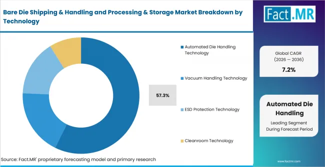
Bare Die Shipping & Handling And Processing & Storage Market Analysis By Technology | Source: Fact.MR
Automated technology leads because semiconductor assembly requires repeatable die placement at production speed. Manual transfer adds variation in positioning and increases physical interaction with ESD-sensitive components.
Robotic pick-and-place equipment can control movement while machine vision verifies die location and orientation. Automation also allows handling data to be connected with production records when individual dies move through several process steps.
Brooks Automation describes semiconductor automation systems that combine material handling with identification and environmental control. Its interface systems support handling and transfer between process stages while reducing contamination exposure, illustrating why automation is increasingly integrated with semiconductor material movement.
Why do Integrated Handling Platforms lead Formulation?
Integrated Handling Platforms are projected to account for a 63.8% share in 2026.
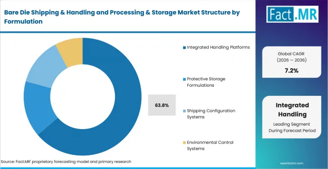
Bare Die Shipping & Handling And Processing & Storage Market Analysis By Formulation | Source: Fact.MR
Integrated platforms lead because die movement cannot be separated completely from identification and storage control in automated manufacturing. A handling system may need to recognize the carrier, retrieve the correct process recipe and transfer the die without changing its orientation.
Hardware-software integration allows movement records to remain connected with manufacturing information. This becomes useful in multi-die packaging, where traceability must be maintained across several components entering the same final assembly.
Semiconductor interface automation already combines handling with material identification and controlled environments. Brooks Automation notes that such systems coordinate movement across semiconductor manufacturing processes while supporting material tracking.
Why does Direct Semiconductor Sales lead Distribution Channel?
Direct Semiconductor Sales are projected to account for a 45.6% share in 2026.
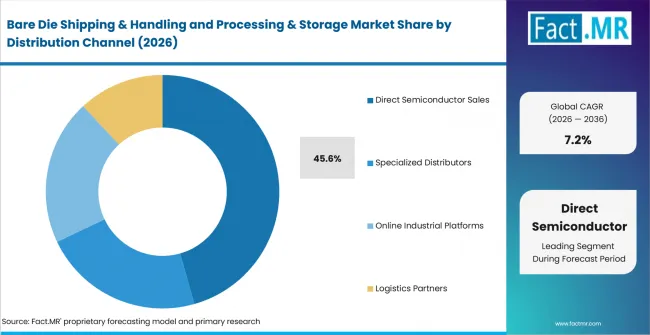
Bare Die Shipping & Handling And Processing & Storage Market Analysis By Distribution Channel | Source: Fact.MR
Direct sales lead because bare die handling products frequently require technical qualification against a semiconductor manufacturer’s equipment and device specifications. Buyers may specify die dimensions, pocket geometry or static-control properties according to the production process.
Automation creates another qualification layer because trays or carriers must move correctly through robotic equipment. A small dimensional mismatch can affect pickup accuracy or introduce additional handling.
Direct supplier relationships allow semiconductor manufacturers to coordinate these specifications before volume deployment. Entegris, for example, supplies bare die trays with selectable configurations and positions them for manual and automated handling, illustrating the application-specific nature of procurement.
What is accelerating Bare Die Shipping & Handling and Processing & Storage Market adoption, and what is holding it back?
Drivers Impact Analysis
| Driver | (~) % Impact on CAGR | Geographic Relevance | Impact Timeline |
|---|---|---|---|
| Expansion of advanced packaging and die-level processing | +1.6% | Global | Short term (≤ 2 years) |
| ESD and contamination-control requirements | +1.4% | USA, Germany and UK | Short term (≤ 2 years) |
| Automation of die transfer and traceability | +1.1% | Global | Medium term (2–4 years) |
| Custom carrier and storage specification | +0.9% | USA, UK and Canada | Medium term (2–4 years) |
| Higher semiconductor manufacturing throughput | +0.6% | Global | Long term (≥ 4 years) |
Source: Fact.MR analysis. Updated Aug 13, 2026
Opportunity Impact Analysis
| Opportunity | (~) % Impact on CAGR | Geographic Relevance | Impact Timeline |
|---|---|---|---|
| Heterogeneous integration and chiplet workflows | +1.0% | Global | Medium term (2–4 years) |
| Specialized ESD-safe bare die carriers | +0.8% | USA, UK and Germany | Medium term (2–4 years) |
| Integrated handling and storage platforms | +0.7% | Global | Long term (≥ 4 years) |
| Standards-aligned packaging and clean handling | +0.5% | USA, Canada and Singapore | Long term (≥ 4 years) |
Source: Fact.MR analysis. Updated Aug 13, 2026
Restraints Impact Analysis
| Restraint | (~) % Impact on CAGR | Geographic Relevance | Impact Timeline |
|---|---|---|---|
| Precision equipment and cleanroom integration cost | -1.1% | Global | Short term (≤ 2 years) |
| Qualification and ESD compliance checks | -0.9% | USA, UK and Germany | Short term (≤ 2 years) |
| Substitution by lower-cost generic carriers | -0.7% | Import-dependent markets | Medium term (2–4 years) |
| Semiconductor capital-spending and input-price pressure | -0.5% | Global | Long term (≥ 4 years) |
Source: Fact.MR analysis. Updated Aug 13, 2026
Which countries are scaling the Bare Die Shipping & Handling and Processing & Storage Market?
- USA: Domestic semiconductor manufacturing and advanced packaging investment is increasing the number of local die-processing workflows. The U.S. National Advanced Packaging Manufacturing Program is supporting equipment and process development intended to move advanced packaging technologies from research into manufacturing, creating demand for controlled die transfer and storage.
- UK: The UK semiconductor strategy emphasizes compound semiconductors, research and chip design rather than high-volume silicon fabrication. These activities create demand for flexible handling and protected storage suited to pilot production and specialist device workflows.
- France: Expansion of semiconductor manufacturing at Crolles increases the downstream requirement for handling and packaging infrastructure. The STMicroelectronics and GlobalFoundries facility is planned around 300 mm wafer production, creating additional device flows into inspection and assembly.
- Germany: New semiconductor capacity in Dresden supports demand for die handling within automotive and industrial semiconductor supply chains. The European Commission has granted designated status under the EU Chips Act to both ESMC and Infineon semiconductor facilities in Germany.
- Italy: New investment is placing greater emphasis on semiconductor back-end activity. The Silicon Box project in Novara is specifically focused on chiplet integration, advanced packaging and testing, creating a direct requirement for controlled die-level movement.
- South Korea: Memory investment continues to support semiconductor equipment demand, particularly for HBM. Multi-die memory architectures increase handling intensity as several dies are stacked and assembled within one device.
- Japan: Continued semiconductor manufacturing investment supports demand for controlled handling across specialty and advanced devices. Government policy remains focused on strengthening domestic semiconductor production infrastructure and supply-chain resilience.
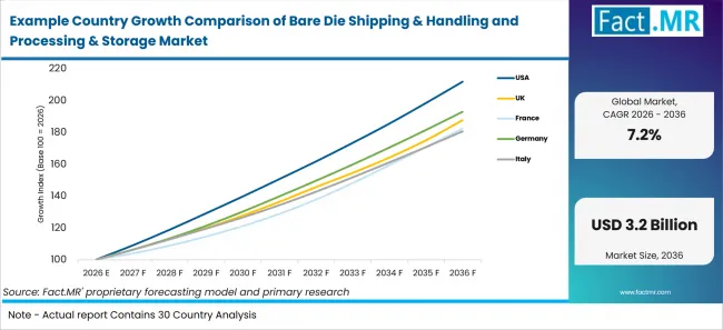
Example Country Growth Comparison Of Bare Die Shipping & Handling And Processing & Storage Market | Source: Fact.MR
| Country | CAGR (2026-2036) |
|---|---|
| USA | 7.8% |
| UK | 6.5% |
| France | 6.2% |
| Germany | 6.8% |
| Italy | 6.1% |
| South Korea | 7.2% |
| Japan | 6.7% |
Source: Fact.MR analysis. Updated Aug 13, 2026
What is driving USA’s growth through 2036?
The USA is forecast to expand at a 7.8% CAGR from 2026 to 2036.
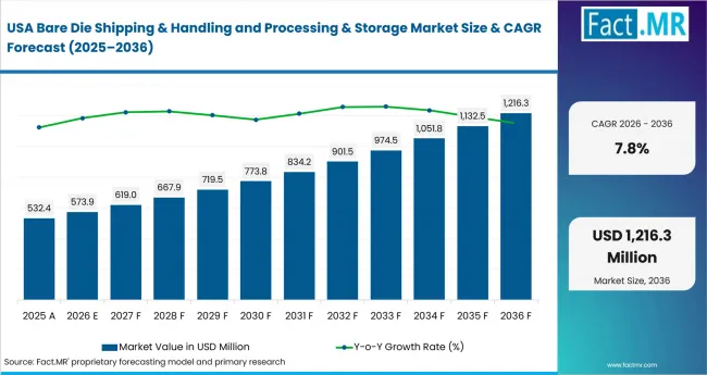
Bare Die Shipping & Handling And Processing & Storage Market Country Value Analysis | Source: Fact.MR
Growth is supported by new semiconductor fabrication and packaging investment that increases domestic movement of wafers and dies between processing stages. In July 2026, the U.S. Department of Commerce announced support for expansion of silicon carbide semiconductor production in California, including new cleanroom space and manufacturing capacity.
Advanced packaging creates an additional demand mechanism. U.S. programmes are funding pilot-scale packaging infrastructure intended to connect research with commercial manufacturing. These facilities require equipment for die positioning and temporary storage before integration into multi-chip packages.
What is driving the UK’s growth through 2036?
The UK is forecast to expand at a 6.5% CAGR from 2026 to 2036.
Growth is linked to specialist semiconductor research and compound-semiconductor activity rather than large silicon fabs. These environments require handling systems that can accommodate varied device dimensions and shorter production runs without sacrificing contamination or ESD control.
A semiconductor facility opened at the University of Southampton in 2025 with electron-beam lithography capability and access to an academic cleanroom. Expansion of research infrastructure creates demand for reusable carriers and controlled storage used while prototype devices move between fabrication and characterization.
What is driving France’s growth through 2036?
France is forecast to expand at a 6.2% CAGR from 2026 to 2036.
France is adding semiconductor production capacity through the STMicroelectronics and GlobalFoundries project at Crolles. The facility is intended for 300 mm semiconductor production and is expected to reach approximately 620,000 wafers annually at full capacity.
Higher wafer throughput increases downstream die volumes entering test and packaging. Suppliers of trays and storage systems can therefore serve flows between fabrication facilities and assembly partners while maintaining protection during transport.
What is driving Germany’s growth through 2036?
Germany is forecast to expand at a 6.8% CAGR from 2026 to 2036.
Germany is expanding semiconductor manufacturing in Dresden through ESMC and Infineon. The ESMC open foundry is expected to reach 480,000 wafers annually by 2029, while Infineon’s designated facility covers power and analog or mixed-signal semiconductor production.
These devices serve automotive and industrial applications where traceability and component reliability are important during downstream processing. Higher production therefore increases demand for controlled carriers that move dies from manufacturing into test and packaging operations.
What is driving Italy’s growth through 2036?
Italy is forecast to expand at a 6.1% CAGR from 2026 to 2036.
Italy is increasing its role in semiconductor back-end processing. In March 2026, the Ministry of Enterprises and Made in Italy signed a development agreement for the Silicon Box project in Novara, which is focused on back-end processing, advanced packaging and testing.
Chiplet integration is particularly relevant to bare die handling because several dies must be stored and positioned before final assembly. Expansion of this production model creates demand for ESD-protected trays and automated transfer technologies near packaging facilities.
What is driving South Korea’s growth through 2036?
South Korea is forecast to expand at a 7.2% CAGR from 2026 to 2036.
South Korea’s semiconductor manufacturing base is closely linked to advanced memory production. SEMI reported that Korea’s semiconductor equipment spending is being supported by HBM investment, which uses vertically integrated die structures for AI-related memory applications.
The handling requirement grows with die stacking because individual memory dies must remain protected before bonding. Automated positioning and stable temporary storage can reduce handling variability when several dies are assembled into an HBM package.
SEMI previously projected South Korean semiconductor manufacturing capacity at 5.4 million wafers per month in 2025, supported by continued memory and foundry activity.
What is driving Japan’s growth through 2036?
Japan is forecast to expand at a 6.7% CAGR from 2026 to 2036.
Japan is strengthening domestic semiconductor production as part of its semiconductor revitalization policy. Government statements in 2026 continued to emphasize reinforcement of semiconductor manufacturing sites and supply-chain resilience.
The country also retains substantial wafer-fabrication capacity. SEMI projected Japanese semiconductor manufacturing capacity at approximately 4.7 million wafers per month in 2025. Continued output creates demand for handling systems used between wafer processing, die testing and downstream assembly.
Who leads the Bare Die Shipping & Handling and Processing & Storage Market?
Entegris, Inc. is positioned as the leading company through its semiconductor materials-handling portfolio. Its bare die tray systems are designed around device retention and compatibility with both manual and automated handling, addressing shipping and storage requirements before final semiconductor packaging.
3M Company competes through semiconductor carrier materials and ESD-protective packaging formats. Its polycarbonate carrier products are designed for semiconductor components requiring static-discharge protection and mechanical protection during transport.
Brooks Automation, Inc. participates through semiconductor automation systems that manage material transfer and identification within manufacturing environments. Automated interfaces become more relevant as semiconductor plants seek repeatable movement with lower contamination exposure.
Kostat, Inc., ITW ECPS, Dalau, Daitron Incorporated, Achilles USA, Inc. and TT Engineering & Manufacturing Sdn Bhd broaden competition across semiconductor handling and related processing requirements.
Supplier selection depends on die retention and ESD properties. Compatibility with automated equipment also influences qualification. Customers additionally assess dimensional consistency and cleanroom suitability when carriers move repeatedly between process steps.
Which companies are the key providers?
Key companies include Entegris, Inc.; 3M Company; Brooks Automation, Inc.; Kostat, Inc.; ITW ECPS; Dalau; Daitron Incorporated; Achilles USA, Inc.; and TT Engineering & Manufacturing Sdn Bhd.
- Entegris, Inc.
- 3M Company
- Brooks Automation, Inc.
- Kostat, Inc.
- ITW ECPS
- Dalau
- Daitron Incorporated
- Achilles USA, Inc.
- TT Engineering & Manufacturing Sdn Bhd
Bibliography
- Brooks Automation. (2026). Interface Automation. Brooks Automation.
- Department for Science, Innovation and Technology, United Kingdom. (2023). National Semiconductor Strategy. UK Government.
- Department for Science, Innovation and Technology, United Kingdom. (2025). European-first Semiconductor Facility Launches in Southampton. UK Government.
- EOS/ESD Association, Inc. (2026). EOS/ESD Fundamentals Part 1: An Introduction to ESD. EOS/ESD Association.
- EOS/ESD Association, Inc. (2026). EOS/ESD Fundamentals Part 6: ESD Standards. EOS/ESD Association.
- European Commission. (2023). State Aid: French Measure Supporting STMicroelectronics and GlobalFoundries Semiconductor Facility in Crolles. European Commission.
- European Commission. (2025). Milestone in Strengthening Europe’s Semiconductor Manufacturing Capacity under the Chips Act. European Commission.
- Entegris, Inc. (2026). H20 Series Polymer Tray. Entegris.
- Ministry of Economy, Trade and Industry, Japan. (2026). Government Policy on Strengthening Semiconductor Production Sites and Supply Chains. Government of Japan.
- Ministry of Enterprises and Made in Italy. (2026). Silicon Box: Development Agreement for the Novara Site. Government of Italy.
- NIST. (2026). National Advanced Packaging Manufacturing Program. U.S. Department of Commerce.
- SEMI. (2024). Global Semiconductor Fab Capacity Projected to Expand in 2024 and 2025. SEMI.
- SEMI. (2025). Global Semiconductor Equipment Sales Projected to Reach USD 156 Billion in 2027. SEMI.
- SEMI. (2026). Global Semiconductor Equipment Sales Forecast to Reach USD 229 Billion in 2028. SEMI.
- U.S. Department of Commerce. (2025). USD 1.4 Billion in Final Awards to Support the Next Generation of U.S. Semiconductor Advanced Packaging. U.S. Department of Commerce.
This Report Answers
- The report examines demand for bare die shipping, handling and storage systems across the principal product and application categories.
- Segment analysis assesses handling equipment alongside storage and protective material requirements within semiconductor production.
- Country analysis evaluates the USA, UK, France, Germany, Italy, South Korea and Japan.
- Competitive analysis examines semiconductor material-handling suppliers and automation providers serving die-level workflows.
- Application analysis considers ESD protection, contamination control and automation requirements across semiconductor manufacturing and assembly.
What does the Bare Die Shipping & Handling and Processing & Storage Market cover?
The market covers equipment, carriers and protective systems used to move and store unpackaged semiconductor dies before final packaging or integration.
The assessment includes bare die handling systems, shipping systems and storage equipment. It also covers die-protection materials and automated technologies used to maintain component condition during semiconductor manufacturing and assembly.
What is included in the scope?
The scope includes vacuum and mechanical die handling equipment used for controlled transfer after wafer processing. Shipping coverage includes reel and tray systems together with tape-based configurations used to protect semiconductor devices during internal or external movement.
Storage coverage includes dry cabinets and cleanroom storage systems designed for intermediate holding before testing or assembly. ESD-protection materials and environmental-control systems are included where they are used specifically for bare die.
Demand from semiconductor foundries and outsourced semiconductor assembly operations is included within the stated segmentation. Electronics OEMs and automotive electronics suppliers are also covered where they purchase systems for bare-die processing or integration.
What is excluded from the scope?
The scope excludes conventional packaging sold for fully encapsulated integrated circuits when it is not intended for bare-die handling.
Front-end semiconductor production equipment such as deposition or lithography tools is excluded unless the equipment performs a die-handling function within the stated segmentation.
General warehouse storage and standard freight packaging are outside the market when they do not provide semiconductor-specific protection or handling capability. Complete semiconductor manufacturing lines are not counted as bare die handling systems solely because they include an internal transfer mechanism.
How Was the Analysis Built?
The analysis draws on more than 120 sources, over 35 company portfolios and more than 20 industry interviews across at least 25 countries.
- Primary Research: Interviews with semiconductor manufacturers, OSAT providers, handling-system suppliers and packaging engineers examine carrier selection, ESD requirements and automation compatibility.
- Desk Research: The review covers semiconductor production capacity, advanced packaging activity and ESD standards. Government semiconductor programmes, industry-body publications and company technical documentation are used where relevant.
- Market Sizing and Forecasting: Estimates combine semiconductor production volumes with die-level processing intensity and packaging activity. The model considers handling equipment installations, replacement demand and storage requirements across major manufacturing regions.
- Data Validation and Update Cycle: Findings are checked against semiconductor-capacity expansion and packaging investment. Updates incorporate changes in advanced packaging adoption, manufacturing investment and die-handling technology.
Segmentation
What is the report's scope and coverage?
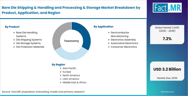
Bare Die Shipping & Handling And Processing & Storage Market Breakdown By Product, Application, And Region | Source: Fact.MR
| Attribute | Details |
|---|---|
| Quantitative Units | USD Billion |
| Market Definition | Systems and materials used to ship, handle, process and store unpackaged semiconductor dies before final integration or packaging |
| Segments Covered | Product; Application; End Use; Technology; Formulation; Distribution Channel |
| Regions Covered | North America; Latin America; Europe; East Asia; South Asia and Pacific; Middle East and Africa |
| Countries Covered | USA; UK; France; Germany; Italy; South Korea; Japan |
| Key Companies Profiled | Entegris, Inc.; 3M Company; Brooks Automation, Inc.; Kostat, Inc.; and others |
| Forecast Period | 2026 to 2036 |
| Approach | Hybrid top-down and bottom-up approach using semiconductor production, die-level processing volumes, packaging and test activity, handling-system installations, storage requirements and supplier portfolio review |
Source: Fact.MR analysis. Updated Aug 13, 2026
How is the market segmented?
-
By Product:
- Bare Die Handling Systems
- Vacuum Pick and Place Systems
- Mechanical Die Handling Systems
- Die Shipping Systems
- Reel and Tray Shipping Systems
- Tape and Reel Systems
- Die Storage Systems
- Dry Storage Cabinets
- Cleanroom Storage Systems
- Die Protection Materials
- ESD Protection Materials
- Encapsulation Materials
- Bare Die Handling Systems
-
By Application:
- Semiconductor Manufacturing
- Wafer Fabrication Processes
- Chip Packaging Applications
- Electronics Assembly
- PCB Assembly Applications
- Device Integration Applications
- Automotive Electronics
- ECU Manufacturing Applications
- EV Electronics Applications
- Consumer Electronics
- Mobile Device Manufacturing
- Home Electronics Manufacturing
- Semiconductor Manufacturing
-
By End Use:
- Semiconductor Foundries
- Integrated Device Manufacturers
- Pure Play Foundries
- Outsourced Semiconductor Assembly
- OSAT Providers
- Contract Manufacturing Units
- Electronics OEMs
- Consumer Electronics OEMs
- Industrial Electronics OEMs
- Automotive Electronics Suppliers
- Tier 1 Suppliers
- EV Component Manufacturers
- Semiconductor Foundries
-
By Technology:
- Automated Die Handling Technology
- Robotic Pick and Place Systems
- Vision Guided Handling Systems
- Vacuum Handling Technology
- Micro Vacuum Systems
- Adaptive Vacuum Control
- ESD Protection Technology
- Static Dissipation Systems
- Charge Neutralization Systems
- Cleanroom Technology
- Contamination Control Systems
- Ultra Clean Handling Systems
- Automated Die Handling Technology
-
By Formulation:
- Integrated Handling Platforms
- Hardware Software Integrated Systems
- Modular Handling Architectures
- Protective Storage Formulations
- ESD Safe Material Systems
- Barrier Protection Systems
- Shipping Configuration Systems
- Tray Based Configurations
- Tape Based Configurations
- Environmental Control Systems
- Controlled Atmosphere Storage
- Temperature Stabilized Systems
- Integrated Handling Platforms
-
By Distribution Channel:
- Direct Semiconductor Sales
- OEM Direct Procurement
- Enterprise Sales Programs
- Specialized Distributors
- Semiconductor Equipment Distributors
- Electronics Material Distributors
- Online Industrial Platforms
- B2B Semiconductor Marketplaces
- Manufacturer Direct Portals
- Logistics Partners
- Specialized Semiconductor Logistics
- Global Freight Operators
- Direct Semiconductor Sales
-
By Region :
- North America
- Latin America
- Western Europe
- Eastern Europe
- East Asia
- South Asia and Pacific
- Middle East & Africa
Frequently Asked Questions
Which Product leads the market?
Which Application leads the market?
Which End Use leads the market?
Which Technology leads the market?
Which Formulation leads the market?
Which Distribution Channel leads the market?
Which country records a 7.8% CAGR?
Which companies are included in the market assessment?
Who worked on this report


Preview the report firsthand - request a free sample
Free SampleGet the brochure for pricing and purchase details
Download PDF