- Market Value (2025): USD 172.4 Mn
- Estimated Value (2026): USD 199.0 Mn
- Forecast Value (2036): USD 830.0 Mn
- CAGR (2026-2036): 15.4%
What is the In-Situ Overlay Bonders Market forecast to be worth by 2036?
USD 199.0 million in 2026 to USD 830.0 million by 2036, at a 15.4% CAGR.
- The In-Situ Overlay Bonders Market crossed a valuation of USD 172.4 million in 2025, supported by demand from Foundries serving Hybrid bonding workflows that require measuring and correcting sub-100 nm alignment error while thermal distortion and wafer or die deformation continue to change during bonding.
- Demand is projected to increase from USD 199.0 million in 2026 to USD 830.0 million by 2036.
- The market is forecast to record a 15.4% CAGR from 2026 to 2036 as alignment requirements, measured machine capability and why in-situ matters physically remain central purchase reasons.
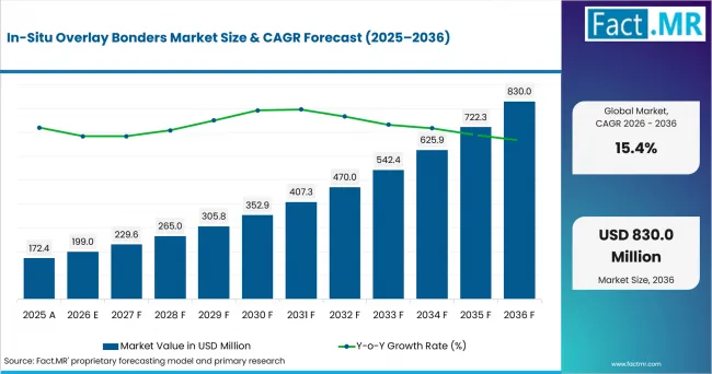
In Situ Overlay Bonders Market Value Analysis | Source: Fact.MR
What are the defining numbers behind In-Situ Overlay Bonders Market growth?
USD 631.0 million absolute opportunity is expected by 2036.
- Demand Drivers in the Market
- Alignment requirements: Sub-100 nm, and in some cases sub-50 nm, alignment specifications are becoming table stakes for hybrid-bonding tool selection: SUSS's Thomas Schmidt notes that alignment must be even better than 100 nm, sometimes 50 nm, and must be precise and repeatable bond to bond, accurate across the full measurement sequence. [1]
- Measured machine capability: Independent machine-capability testing is becoming a purchase gate: Imec/BESI matrix baseline machine capability (MBMC) testing on a BESI Chameo Ultra Plus demonstrated alignment well below 200 nm at 3-sigma on glass-on-glass, and under 200 nm residual worst-corner error on real die-to-wafer bonding with temporary bonding material, giving buyers a documented benchmark to specify against. [2]
- Why in-situ matters physically: Static pre-measurement cannot capture how a die actually lands, which is pushing demand toward true in-situ correction: adhesive/TBM dies relax after vacuum release while SiCN dielectric hybrid bonds lock in strain, so final misalignment sums dielectric/thickness effects with bending strain, and only measurement at the moment of bonding sees the true landed state.
- Thermocompression analog: Thermocompression bonding provides a parallel proof point for real-time correction: alignment requirements of plus-or-minus 1 micrometer or tighter, with some processes demanding sub-500 nm precision, collide with thermal drift at 250-400 degrees C that exceeds those tolerances, pushing buyers toward active, real-time correction loops rather than static offsets. [3]
- Key Segments Analyzed
- By Overlay Sensing: IR through-wafer imaging is projected to hold 32.0% share in 2026, supported by a clear process advantage: Infrared through-wafer imaging can observe alignment marks through silicon while the substrates remain in the bond tool. This makes it suitable for measuring the relative position that actually exists immediately before contact.
- By Correction Mode: Real-time closed loop is projected to hold 42.3% share in 2026, supported by a clear process advantage: A real-time closed loop measures residual error and adjusts the stage before the bond is committed. It can respond to drift, local distortion and thermal change that were not fully represented in a prior calibration map.
- By Overlay Accuracy: <100 nm is projected to hold 38.3% share in 2026, supported by a clear process advantage: Sub-100 nanometer overlay protects contact area as hybrid-bond pitches move toward the low-micrometer and sub-micrometer range. The tighter class also provides process margin for wafer distortion and metrology uncertainty.
- By Bond Type: Hybrid bonding is projected to hold 46.8% share in 2026, supported by a clear process advantage: Hybrid bonding requires the dielectric surfaces and copper pads to register at the same interface. Misalignment can therefore create both mechanical discontinuity and electrical opens, increasing the value of in-situ correction.
- By End User: Foundries are projected to hold 30.2% share in 2026, supported by a clear process advantage: Foundries support heterogeneous devices, multiple customer layouts and successive pitch reductions, which makes reusable in-situ correction models commercially valuable. Their qualification burden is not one package but a portfolio of advanced integration flows.
- Analyst Opinion at Fact.MR
- Shambhu Nath Jha, Sr. Consultant at Fact.MR, states, 'Buyers should evaluate the complete process sequence around measuring and correcting sub-100 nm alignment error while thermal distortion and wafer or die deformation continue to change during bonding. Technical review should focus on repeatability, integration, defect control and production throughput rather than a single headline specification. Suppliers that connect tool performance to measurable yield and qualification results are likely to build trust faster.'
- Strategic Implications
- The practical procurement test is repeatable post-bond overlay across the full field and across lots, with a documented correction model for heat, bow and local distortion.
- Equipment suppliers should document how their systems address the challenge of measuring and correcting sub-100 nm alignment error while thermal distortion and wafer or die deformation continue to change during bonding across production-representative wafers, panels, dies or packages.
- Procurement teams can compare process capability, integration burden, service coverage and qualification evidence before prioritizing nominal throughput or a single accuracy claim.
Taiwan is projected to record a 17.0% CAGR as leading foundry production, advanced packaging and a dense OSAT and substrate supply chain supports relevant capital spending; Malaysia is projected to record a 16.4% CAGR as large-scale outsourced assembly, test and package manufacturing supports relevant capital spending; South Korea is projected to record a 16.2% CAGR as high-volume memory, HBM and vertically integrated semiconductor manufacturing supports relevant capital spending; Japan is projected to record a 16.0% CAGR as semiconductor equipment, materials, inspection and memory-process expertise supports relevant capital spending; while USA is projected to record a 16.7% CAGR as leading-edge logic, high-performance computing, federally supported semiconductor R&D and a large domestic equipment base supports relevant capital spending through 2036.
How does the In-Situ Overlay Bonders Market break down by segment?
IR through-wafer imaging leads Overlay Sensing with a 32.0% share, while Real-time closed loop accounts for 42.3% of Correction Mode in 2026.
Why does IR through-wafer imaging lead Overlay Sensing?
IR through-wafer imaging is projected to account for 32.0% share in 2026.
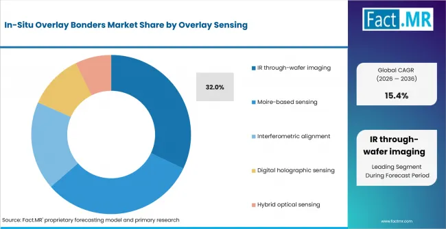
In Situ Overlay Bonders Market Analysis By Overlay Sensing | Source: Fact.MR
IR through-wafer imaging reads alignment marks through silicon, allowing the bonder to measure overlay even when the active surfaces are hidden between stacked wafers. Optical surface inspection works well when marks remain visible, but it becomes less useful once opaque layers, temporary carriers or bonded interfaces block the direct line of sight. Infrared imaging therefore fits 3D integration, MEMS, hybrid bonding and advanced packaging processes where alignment errors of only a few micrometres or less can interrupt electrical contact and reduce device yield. The method also supports non-contact inspection during alignment, which helps limit handling risk before the bond is completed.
Why does Real-time closed loop lead Correction Mode?
Real-time closed loop is projected to account for 42.3% share in 2026.
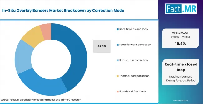
In Situ Overlay Bonders Market Analysis By Correction Mode | Source: Fact.MR
A real-time closed loop measures residual error and adjusts the stage before the bond is committed. It can respond to drift, local distortion and thermal change that were not fully represented in a prior calibration map. Feed-forward correction is faster when errors are stable, but it cannot recover an unmodeled change that develops inside the current bond cycle. In TCB, alignment requirements are ±1 µm or better, with some cutting-edge processes demanding sub-500-nanometer precision, while thermal expansion at 250-400 °C causes drift exceeding those tolerances - motivating active, real-time correction loops in the bonder. [3] Buyers therefore tend to treat real-time closed loop as the practical choice when qualification must balance process capability, repeatability and production economics.
Why does <100 nm lead Overlay Accuracy?
<100 nm is projected to account for 38.3% share in 2026.
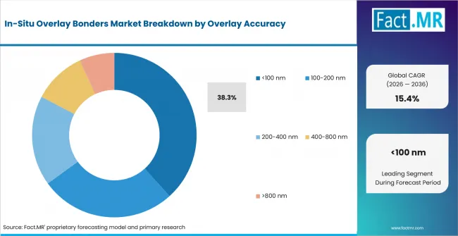
In Situ Overlay Bonders Market Analysis By Overlay Accuracy | Source: Fact.MR
Sub-100 nanometer overlay protects contact area as hybrid-bond pitches move toward the low-micrometer and sub-micrometer range. The tighter class also provides process margin for wafer distortion and metrology uncertainty. The 100-200 nanometer class remains useful for coarser interfaces, but it leaves less margin when pad dimensions and dielectric openings shrink. Imec/BESI IMAPS paper on overlay analysis/optimization for high-accuracy hybrid D2W bonding (machine-baseline capability, residual error decomposition). [2] Buyers therefore tend to treat <100 nm as the practical choice when qualification must balance process capability, repeatability and production economics.
Why does Hybrid bonding lead Bond Type?
Hybrid bonding is projected to account for 46.8% share in 2026.
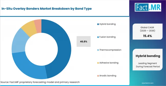
In Situ Overlay Bonders Market Analysis By Bond Type | Source: Fact.MR
Hybrid bonding requires the dielectric surfaces and copper pads to register at the same interface. Misalignment can therefore create both mechanical discontinuity and electrical opens, increasing the value of in-situ correction. Fusion bonding is primarily a dielectric interface and does not impose the same simultaneous copper-pad registration requirement. The same study shows that with adhesive/TBM the die relaxes after vacuum release (soft layer releases strain), whereas with SiCN/SiCN dielectric hybrid bonding the strong dielectric bond locks in strain - final misalignment becomes the SUM of dielectric/thickness effects plus bending strain (~110 nm total expected). Static pre-measurement cannot capture this; only in-situ measurement at the moment of bonding sees the true landed state. Buyers therefore tend to treat hybrid bonding as the practical choice when qualification must balance process capability, repeatability and production economics.
Why do Foundries lead End User?
Foundries are projected to account for 30.2% share in 2026.
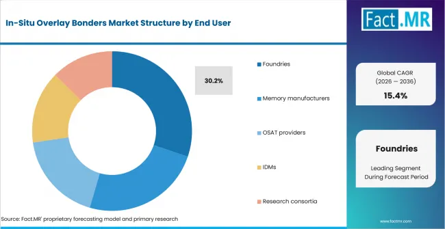
In Situ Overlay Bonders Market Analysis By End User | Source: Fact.MR
Foundries support heterogeneous devices, multiple customer layouts and successive pitch reductions, which makes reusable in-situ correction models commercially valuable. Their qualification burden is not one package but a portfolio of advanced integration flows. Memory manufacturers can optimize around more repetitive stack designs, while foundries need overlay control that transfers across a wider design mix. SUSS's Thomas Schmidt: Alignment must be even better than 100 nm, sometimes even 50 nm. The alignment must be accurate and precise, with repeatable bond-to-bond performance. [1] Buyers therefore tend to treat foundries as the practical choice when qualification must balance process capability, repeatability and production economics.
What is accelerating In-Situ Overlay Bonders Market adoption, and what is holding it back?
The strongest accelerator is alignment requirements, while the main restraint is that higher sensing resolution can reduce throughput and still cannot recover non-correctable die or wafer deformation.
Drivers Impact Analysis
| DRIVER | (~) % IMPACT ON CAGR | GEOGRAPHIC RELEVANCE | IMPACT TIMELINE |
|---|---|---|---|
| Alignment requirements | +4.3% | Global leading-edge fabs | Medium term (2-4 years) |
| Measured machine capability | +3.5% | Global leading-edge fabs | Medium term (2-4 years) |
| Why in-situ matters physically | +2.9% | Global leading-edge fabs | Medium term (2-4 years) |
| Thermocompression analog | +2.3% | Global leading-edge fabs | Medium term (2-4 years) |
Source: Fact.MR analysis. Updated Jul 22, 2026
- Alignment requirements: SUSS's Thomas Schmidt: Alignment must be even better than 100 nm, sometimes even 50 nm. The alignment must be accurate and precise, with repeatable bond-to-bond performance. [1]
- Measured machine capability: Imec/BESI matrix baseline machine capability (MBMC) testing on a BESI Chameo Ultra Plus shows alignment capability well below 200 nm @3σ with glass-on-glass tests; on real D2W bonding with temporary bonding material, <200 nm residual worst-corner error was achieved, with a characteristic ~80 nm die-corner scaling error traced by FEM modeling to pedestal-induced die bending and dielectric/thickness mismatch. [2]
- Why in-situ matters physically: The same study shows that with adhesive/TBM the die relaxes after vacuum release (soft layer releases strain), whereas with SiCN/SiCN dielectric hybrid bonding the strong dielectric bond locks in strain - final misalignment becomes the SUM of dielectric/thickness effects plus bending strain (~110 nm total expected).
- Thermocompression analog: In TCB, alignment requirements are ±1 µm or better, with some cutting-edge processes demanding sub-500-nanometer precision, while thermal expansion at 250-400 °C causes drift exceeding those tolerances - motivating active, real-time correction loops in the bonder. [3]
Opportunity Impact Analysis
| OPPORTUNITY | (~) % IMPACT ON CAGR | GEOGRAPHIC RELEVANCE | IMPACT TIMELINE |
|---|---|---|---|
| Feedback from external metrology/litho scanners | +2.6% | Global leading-edge fabs | Medium term (2-4 years) |
| Distortion mapping, not just rigid alignment | +2.0% | Global leading-edge fabs | Medium term (2-4 years) |
| IR alignment through silicon | +1.5% | Global leading-edge fabs | Medium term (2-4 years) |
Source: Fact.MR analysis. Updated Jul 22, 2026
- Feedback from external metrology/litho scanners: EV Group explicitly describes feedforward/feedback loops between bonders and off-tool metrology or lithography scanners - bonding overlay is becoming a litho-style APC (advanced process control) discipline.
- Distortion mapping, beyond rigid alignment: Modern systems measure intra-die scaling (magnification) and non-linear distortion, beyond 3-parameter X/Y/θ - required because thin (<50 µm) chiplets bend under vacuum collets (SMTA paper, §10).
Restraints Impact Analysis
| RESTRAINT | (~) % IMPACT ON CAGR | GEOGRAPHIC RELEVANCE | IMPACT TIMELINE |
|---|---|---|---|
| Primary qualification constraint | -2.3% | Global leading-edge fabs | Medium term (2-4 years) |
| Alignment and registration risk | -1.8% | Global leading-edge fabs | Medium term (2-4 years) |
| Cross-module integration risk | -1.4% | Global leading-edge fabs | Medium term (2-4 years) |
Source: Fact.MR analysis. Updated Jul 22, 2026
- Primary qualification constraint: Higher sensing resolution can reduce throughput and still cannot recover non-correctable die or wafer deformation.
- Alignment and registration risk: The same study shows that with adhesive/TBM the die relaxes after vacuum release (soft layer releases strain), whereas with SiCN/SiCN dielectric hybrid bonding the strong dielectric bond locks in strain - final misalignment becomes the SUM of dielectric/thickness effects plus bending strain (~110 nm total expected).
- Cross-module integration risk: The process must be qualified across adjacent modules because a local improvement can still fail the full flow when measuring and correcting sub-100 nm alignment error while thermal distortion and wafer or die deformation continue to change during bonding.
Which countries are scaling In-Situ Overlay Bonders Market fastest?
Japan is projected to record a 16.0% CAGR for In Situ Overlay Bonders Market as semiconductor equipment, materials, inspection and memory-process expertise.
- Countries differ less by the headline CAGR than by the type of semiconductor work creating demand for the In-Situ Overlay Bonders Market.
- Taiwan follows a pathway shaped by leading foundry production, advanced packaging and a dense OSAT and substrate supply chain. China takes a different path through rapid domestic capacity build-out, local-equipment substitution and tighter access to controlled foreign tools.
- USA and Malaysia remain aligned through distinct combinations of device production, equipment development and advanced packaging investment.
- South Korea develops through high-volume memory, HBM and vertically integrated semiconductor manufacturing, while Japan relies on semiconductor equipment, materials, inspection and memory-process expertise.
- Markets with similar CAGRs can follow different development paths because installed fabs, device mix, local equipment capability, export controls and qualification cycles differ.
The full report compares the six named country markets within the wider regional coverage of North America, Latin America, Europe, East Asia, South Asia & Oceania, and the Middle East & Africa.
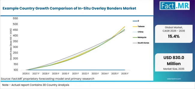
Example Country Growth Comparison Of In Situ Overlay Bonders Market | Source: Fact.MR
| COUNTRY | CAGR, 2026 to 2036 |
|---|---|
| Taiwan | 17.0% |
| USA | 16.7% |
| Malaysia | 16.4% |
| South Korea | 16.2% |
| Japan | 16.0% |
Source: Fact.MR analysis. Updated Jul 22, 2026
What is driving Taiwan's growth through 2036?
17.0% CAGR, supported by leading foundry production, advanced packaging and a dense OSAT and substrate supply chain.
Taiwan combines leading foundry production, advanced packaging and a dense OSAT and substrate supply chain with a 40.6% share of 2026 demand across the six profiled countries. EV Group explicitly describes feedforward/feedback loops between bonders and off-tool metrology or lithography scanners - bonding overlay is becoming a litho-style APC (advanced process control) discipline. The commercial link is the need to solve the problem of measuring and correcting sub-100 nm alignment error while thermal distortion and wafer or die deformation continue to change during bonding as capacity and process complexity increase.
What is driving USA's growth through 2036?
16.7% CAGR, supported by leading-edge logic, high-performance computing, federally supported semiconductor R&D and a large domestic equipment base.
USA combines leading-edge logic, high-performance computing, federally supported semiconductor R&D and a large domestic equipment base with a 8.2% share of 2026 demand across the six profiled countries. EV Group explicitly describes feedforward/feedback loops between bonders and off-tool metrology or lithography scanners - bonding overlay is becoming a litho-style APC (advanced process control) discipline. The commercial link is the need to solve the problem of measuring and correcting sub-100 nm alignment error while thermal distortion and wafer or die deformation continue to change during bonding as capacity and process complexity increase.
What is driving Malaysia's growth through 2036?
16.4% CAGR, supported by large-scale outsourced assembly, test and package manufacturing.
Malaysia combines large-scale outsourced assembly, test and package manufacturing with a 13.6% share of 2026 demand across the six profiled countries. SUSS's Thomas Schmidt: Alignment must be even better than 100 nm, sometimes even 50 nm. [1] The commercial link is the need to solve the problem of measuring and correcting sub-100 nm alignment error while thermal distortion and wafer or die deformation continue to change during bonding as capacity and process complexity increase.
What is driving South Korea's growth through 2036?
16.2% CAGR, supported by high-volume memory, HBM and vertically integrated semiconductor manufacturing.
South Korea combines high-volume memory, HBM and vertically integrated semiconductor manufacturing with a 13.4% share of 2026 demand across the six profiled countries. Imec/BESI matrix baseline machine capability (MBMC) testing on a BESI Chameo Ultra Plus shows alignment capability well below 200 nm @3σ with glass-on-glass tests; on real D2W bonding with temporary bonding material, <200 nm residual worst-corner error was achieved, with a characteristic ~80 nm die-corner scaling error traced by FEM modeling to. [2] The commercial link is the need to solve the problem of measuring and correcting sub-100 nm alignment error while thermal distortion and wafer or die deformation continue to change during bonding as capacity and process complexity increase.
What is driving Japan's growth through 2036?
16.0% CAGR, supported by semiconductor equipment, materials, inspection and memory-process expertise.
Japan combines semiconductor equipment, materials, inspection and memory-process expertise with a 8.5% share of 2026 demand across the six profiled countries. The same study shows that with adhesive/TBM the die relaxes after vacuum release (soft layer releases strain), whereas with SiCN/SiCN dielectric hybrid bonding the strong dielectric bond locks in strain - final misalignment becomes the SUM of dielectric/thickness effects plus bending strain (~110 nm total expected). The commercial link is the need to solve the problem of measuring and correcting sub-100 nm alignment error while thermal distortion and wafer or die deformation continue to change during bonding as capacity and process complexity increase.
Who leads the In-Situ Overlay Bonders Market?
EV Group and SUSS MicroTec lead the competitive landscape, followed by BESI and ASMPT as the next tier of challengers.
EV Group participates through wafer bonding, activation and cluster-integrated process control. APC loops, distortion control, mini-environment particle management integrated with in-situ monitoring. SUSS MicroTec participates through wafer alignment, bonding and advanced-packaging lithography, with relevance determined by its ability to address the challenge of measuring and correcting sub-100 nm alignment error while thermal distortion and wafer or die deformation continue to change during bonding. BESI participates through high-accuracy die placement and hybrid-bonding assembly. Chameo Ultra Plus; joint development with imec quantifying residual non-correctable errors and FEM-modeled die bending. ASMPT participates through die placement, thermocompression bonding and packaging automation, with relevance determined by its ability to address the challenge of measuring and correcting sub-100 nm alignment error while thermal distortion and wafer or die deformation continue to change during bonding.
Competition is expected to center on repeatable process performance, integration with adjacent modules, installed-base service and documented capability to address the challenge of measuring and correcting sub-100 nm alignment error while thermal distortion and wafer or die deformation continue to change during bonding. Buyers are likely to compare accuracy, defect prevention, throughput, recipe stability and the completeness of the delivered process cell.
Which companies are the key providers?
Key companies include EV Group; SUSS MicroTec; BESI; ASMPT.
- EV Group
- SUSS MicroTec
- BESI
- ASMPT
What is the report's scope and coverage?
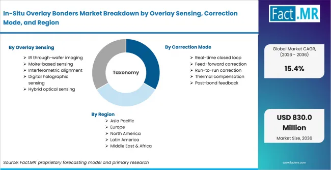
In Situ Overlay Bonders Market Breakdown By Overlay Sensing, Correction Mode, And Region | Source: Fact.MR
| Attribute | Details |
|---|---|
| Quantitative Units | USD 199.0 million in 2026 to USD 830.0 million by 2036 at a 15.4% CAGR |
| Market Definition | In-situ overlay bonders are die/wafer bonders that measure and correct overlay (X, Y, θ, and intra-die scaling/distortion) inside the bonder, during or immediately before the bond event, using integrated IR/optical metrology and closed-loop actuation - as opposed to relying on off-line metrology and static recipe offsets. The segment is defined by alignment capability at or below ~200 nm (3σ) for die-to-wafer and <100 nm, in some cases <50 nm, for wafer-to-wafer hybrid bonding. |
| Overlay Sensing | IR through-wafer imaging; Moire-based sensing; Interferometric alignment; Digital holographic sensing; Hybrid optical sensing |
| Correction Mode | Real-time closed loop; Feed-forward correction; Run-to-run correction; Thermal compensation; Post-bond feedback |
| Overlay Accuracy | <100 nm; 100-200 nm; 200-400 nm; 400-800 nm; >800 nm |
| Bond Type | Hybrid bonding; Fusion bonding; Thermocompression; Adhesive bonding; Anodic bonding |
| End User | Foundries; Memory manufacturers; OSAT providers; IDMs; Research consortia |
| Regions Covered | North America; Latin America; Europe; East Asia; South Asia & Oceania; Middle East & Africa |
| Countries Covered | Taiwan; China; Malaysia; South Korea; Japan; USA |
| Key Companies Profiled | EV Group; SUSS MicroTec; BESI; ASMPT |
| Forecast Period | 2026 to 2036 |
| Approach | Hybrid top-down and bottom-up approach using demand indicators across Overlay Sensing; Correction Mode; Overlay Accuracy; Bond Type; End User; country-level growth; company participation and adoption trends |
Source: Fact.MR analysis. Updated Jul 22, 2026
Bibliography
- [1] Semiconductor Engineering. (n.d.). Making Hybrid Bonding Better.
- [2] IMAPS. (n.d.). 128385 Overlay Analysis And Optimization For High Accuracy Hybrid D2W Bonding.
- [3] Eureka. (n.d.). Report How To Align Die In Thermocompression Bonding For Precision.
This Report Addresses
- The report provides strategic intelligence on In-Situ Overlay Bonders Market across Overlay Sensing and Correction Mode choices that shape purchasing decisions.
- Segment analysis covers IR through-wafer imaging as the share leader within the 2026 market structure.
- Regional outlook evaluates Taiwan and China alongside Malaysia and South Korea, while Japan and USA complete the growth comparison.
- Competitive analysis profiles EV Group and SUSS MicroTec alongside BESI and ASMPT, followed by additional active providers.
- Use-case assessment covers the categories and applications that shape demand in the In-Situ Overlay Bonders Market across the forecast period.
What does the In-Situ Overlay Bonders Market cover?
The market covers equipment and process systems configured to address the challenge of measuring and correcting sub-100 nm alignment error while thermal distortion and wafer or die deformation continue to change during bonding.
In-situ overlay bonders are die/wafer bonders that measure and correct overlay (X, Y, θ, and intra-die scaling/distortion) inside the bonder, during or immediately before the bond event, using integrated IR/optical metrology and closed-loop actuation - as opposed to relying on off-line metrology and static recipe offsets. The segment is defined by alignment capability at or below ~200 nm (3σ) for die-to-wafer and <100 nm, in some cases <50 nm, for wafer-to-wafer hybrid bonding.
Commercial value arises from the complete configured system, including process control, handling, software and integrated modules required for repeatable operation. Finished semiconductor devices, package value and unrelated parent-market equipment are excluded.
What is included in the scope?
The scope includes systems used by foundries and the other end-user groups listed in the segmentation.
The market is segmented by Overlay Sensing, including IR through-wafer imaging, Moire-based sensing, Interferometric alignment, Digital holographic sensing, Hybrid optical sensing; Correction Mode, including Real-time closed loop, Feed-forward correction, Run-to-run correction, Thermal compensation, Post-bond feedback; Overlay Accuracy, including <100 nm, 100-200 nm, 200-400 nm, 400-800 nm, >800 nm; Bond Type, including Hybrid bonding, Fusion bonding, Thermocompression, Adhesive bonding, Anodic bonding; End User, including Foundries, Memory manufacturers, OSAT providers, IDMs, Research consortia.
Integrated handling, metrology, cleaning, activation, process-control or support modules are included when delivered as part of the configured market system.
What is excluded from the scope?
The scope excludes unrelated semiconductor equipment, standalone materials and components sold independently of the configured system.
It also excludes facility construction, cleanroom infrastructure, the value of processed wafers or packages, and adjacent process steps that are not part of the defined equipment category.
How Was the Analysis Built?
Fact.MR is of the opinion that this assessment combines structured market analysis with a review of public information and industry evidence relevant to the market.
- Market Assessment: The analysis considers demand patterns, supply conditions, segment mix, country activity, company participation, and adoption trends.
- Evidence Review: Public company disclosures, government and regulatory publications, trade information, technical literature, and industry records inform the assessment.
- Validation and Updates: Findings are cross-checked against available market indicators and reviewed when material market developments emerge.
Segmentation
How is the market segmented?
-
By Overlay Sensing:
- IR through-wafer imaging
- Moire-based sensing
- Interferometric alignment
- Digital holographic sensing
- Hybrid optical sensing
-
By Correction Mode:
- Real-time closed loop
- Feed-forward correction
- Run-to-run correction
- Thermal compensation
- Post-bond feedback
-
By Overlay Accuracy:
- <100 nm
- 100-200 nm
- 200-400 nm
- 400-800 nm
- >800 nm
-
By Bond Type:
- Hybrid bonding
- Fusion bonding
- Thermocompression
- Adhesive bonding
- Anodic bonding
-
By End User:
- Foundries
- Memory manufacturers
- OSAT providers
- IDMs
- Research consortia
-
By Region:
- North America
- USA
- Latin America
- Other regional markets assessed at aggregate level
- Europe
- Other regional markets assessed at aggregate level
- East Asia
- Taiwan
- China
- South Korea
- Japan
- South Asia & Oceania
- Malaysia
- Middle East & Africa
- Other regional markets assessed at aggregate level
- North America
Frequently Asked Questions
Which Overlay Sensing leads the In-Situ Overlay Bonders Market?
Which Correction Mode leads the In-Situ Overlay Bonders Market?
Which Overlay Accuracy leads the In-Situ Overlay Bonders Market?
Which Bond Type leads the In-Situ Overlay Bonders Market?
Which End User leads the In-Situ Overlay Bonders Market?
What CAGR is projected for Taiwan in the In-Situ Overlay Bonders Market?
What CAGR is projected for USA in the In-Situ Overlay Bonders Market?
What CAGR is projected for Malaysia in the In-Situ Overlay Bonders Market?
What CAGR is projected for South Korea in the In-Situ Overlay Bonders Market?
What CAGR is projected for Japan in the In-Situ Overlay Bonders Market?
What is the primary driver of the In-Situ Overlay Bonders Market?
What is the main restraint in the In-Situ Overlay Bonders Market?
Who worked on this report


Preview the report firsthand - request a free sample
Free SampleGet the brochure for pricing and purchase details
Download PDF