- Market Value (2025): USD 229.4 Mn
- Estimated Value (2026): USD 262.0 Mn
- Forecast Value (2036): USD 985.0 Mn
- CAGR (2026-2036): 14.2%
What is the Plasma Activation Bonders Market forecast to be worth by 2036?
USD 262.0 million in 2026 to USD 985.0 million by 2036, at a 14.2% CAGR.
- The Plasma Activation Bonders Market crossed a valuation of USD 229.4 million in 2025, supported by demand from Foundries serving Cu-dielectric hybrid surfaces workflows that require creating highly reactive hydrophilic surfaces without plasma damage, particles or an uncontrolled delay before contact.
- Demand is projected to increase from USD 262.0 million in 2026 to USD 985.0 million by 2036.
- The market is forecast to record a 14.2% CAGR from 2026 to 2036 as mechanism, two equipment families and dielectric-specific chemistry remain central purchase reasons.
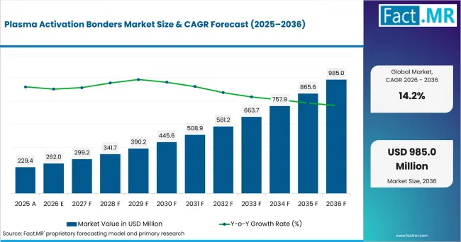
Plasma Activation Bonders Market Value Analysis | Source: Fact.MR
What are the defining numbers behind Plasma Activation Bonders Market growth?
USD 723.0 million absolute opportunity is expected by 2036.
- Demand Drivers in the Market
- Mechanism: Plasma activation works by creating reactive dangling bonds and silanol (-OH) groups on silicon and dielectric surfaces, so demand for these tools tracks the industry's shift toward covalent, low-temperature bonding: van der Waals bonds forming on contact convert to covalent Si-O-Si bridges during a low-temperature anneal, avoiding the above-600 degrees C thermal budgets that would destroy pre-processed CMOS. [1][2]
- Two equipment families: Buyers are choosing between two distinct architectures based on throughput and material needs - atmospheric-pressure PAB (dielectric barrier discharge, corona, or plasma jet, roughly 40-second treatment) and low-pressure PAB (RIE/ICP-RIE or remote plasma at 0.1-100 Pa, 13.56 MHz, 30-60 seconds) - keeping tool selection tied closely to the target material and integration scheme. [2]
- Dielectric-specific chemistry: As hybrid-bonding dielectrics narrow toward SiCN/SiO stacks, demand is shifting to dual-RF capacitively-coupled plasma treatments that hold RMS roughness within 0.1 nm while tuning bonding energy, a process window validated by double-cantilever-beam testing after a 350 degrees C, one-hour anneal in a Sungkyunkwan University study. [3]
- Hybrid bonding flow context: Because the bond front propagates across the entire wafer at room temperature immediately after activation and alignment, followed by a roughly 350 degrees C anneal that converts dielectric hydrogen bonds to covalent bonds while copper fuses, buyers increasingly specify activation modules tightly synchronized with the rest of the hybrid-bonding sequence, per Semiconductor Engineering. [4]
- Key Segments Analyzed
- By Plasma Source: N2 remote plasma is projected to hold 30.0% share in 2026, supported by a clear process advantage: Remote nitrogen plasma supplies reactive species while limiting direct ion bombardment at the wafer surface. That balance is useful when activation must increase bondability without damaging copper, low-k films or exposed polymers.
- By Integration Mode: Cluster-integrated activation is projected to hold 42.3% share in 2026, supported by a clear process advantage: Cluster-integrated activation shortens the interval between plasma exposure and contact and prevents the activated surface from returning to uncontrolled ambient air. It also allows the transfer atmosphere and recipe traceability to be qualified with the bonder.
- By Activation Target: Cu-dielectric hybrid surfaces are projected to hold 37.5% share in 2026, supported by a clear process advantage: Copper-dielectric hybrid surfaces require simultaneous management of metal oxide, dielectric hydrophilicity and surface contamination. The mixed interface therefore creates more process value for a tightly controlled plasma recipe than a dielectric-only target.
- By Wafer Size: 300 mm is projected to hold 42.9% share in 2026, supported by a clear process advantage: The 300 millimeter format aligns with leading logic, memory and advanced-packaging infrastructure, allowing plasma activation to enter production without a separate wafer-size ecosystem. It also spreads uniformity requirements over the largest mainstream wafer area.
- By End User: Foundries are projected to hold 28.6% share in 2026, supported by a clear process advantage: Foundries must qualify activation across multiple dielectric stacks, copper schemes and customer designs, making recipe flexibility and chamber matching central purchase criteria. The same platform can support logic chiplets, image sensors and other heterogeneous flows.
- Analyst Opinion at Fact.MR
- Shambhu Nath Jha, Sr. Consultant at Fact.MR, states, 'Buyers should evaluate the complete process sequence around creating highly reactive hydrophilic surfaces without plasma damage, particles or an uncontrolled delay before contact. Technical review should focus on repeatability, integration, defect control and production throughput rather than a single headline specification. Suppliers that connect tool performance to measurable yield and qualification results are likely to build trust faster.'
- Strategic Implications
- Qualification should cover ion energy, radical chemistry, surface contact angle, queue-time decay and bond-strength uniformity as a single recipe.
- Equipment suppliers should document how their systems address the challenge of creating highly reactive hydrophilic surfaces without plasma damage, particles or an uncontrolled delay before contact across production-representative wafers, panels, dies or packages.
- Procurement teams can compare process capability, integration burden, service coverage and qualification evidence before prioritizing nominal throughput or a single accuracy claim.
Taiwan is projected to record a 15.4% CAGR as leading foundry production, advanced packaging and a dense OSAT and substrate supply chain supports relevant capital spending;South Korea is projected to record a 15.0% CAGR as high-volume memory, HBM and vertically integrated semiconductor manufacturing supports relevant capital spending; Malaysia is projected to record a 15.1% CAGR as large-scale outsourced assembly, test and package manufacturing supports relevant capital spending; Singapore is projected to record a 14.4% CAGR as advanced-packaging R&D, specialty fabs and regional assembly and test operations supports relevant capital spending; while Vietnam is projected to record a 15.8% CAGR as expanding back-end assembly and electronics manufacturing capacity supports relevant capital spending through 2036.
How does the Plasma Activation Bonders Market break down by segment?
N2 remote plasma leads Plasma Source with a 30.0% share, while Cluster-integrated activation accounts for 42.3% of Integration Mode in 2026.
Why does N2 remote plasma lead Plasma Source?
N2 remote plasma is projected to account for 30.0% share in 2026.
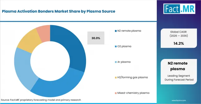
Plasma Activation Bonders Market Analysis By Plasma Source | Source: Fact.MR
Remote nitrogen plasma supplies reactive species while limiting direct ion bombardment at the wafer surface. That balance is useful when activation must increase bondability without damaging copper, low-k films or exposed polymers. Oxygen plasma is effective for hydrophilizing oxide surfaces, but it can accelerate copper oxidation and may require tighter material-specific control. Atmospheric-pressure PAB (dielectric barrier discharge, corona, plasma jet; ~40 s treatment, synthetic air or O2 for Si; Ar/H2 or humid O2 for glass/LiTaO3) vs. low-pressure PAB (RIE/ICP-RIE/remote plasma at 0.1-100 Pa, 13.56 MHz, 30-60 s). [2] Buyers therefore tend to treat N2 remote plasma as the practical choice when qualification must balance process capability, repeatability and production economics.
Why does Cluster-integrated activation lead Integration Mode?
Cluster-integrated activation is projected to account for 42.3% share in 2026.
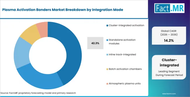
Plasma Activation Bonders Market Analysis By Integration Mode | Source: Fact.MR
Cluster-integrated activation places surface treatment, cleaning, alignment and bonding inside one controlled equipment line, which limits wafer exposure to air between process steps. Standalone activation adds transfer time and raises the risk of surface contamination, moisture uptake or loss of activation strength before bonding begins. The integrated layout also gives manufacturers tighter control over vacuum conditions, process timing and wafer handling across the full bond sequence.
Why do Cu-dielectric hybrid surfaces lead Activation Target?
Cu-dielectric hybrid surfaces are projected to account for 37.5% share in 2026.
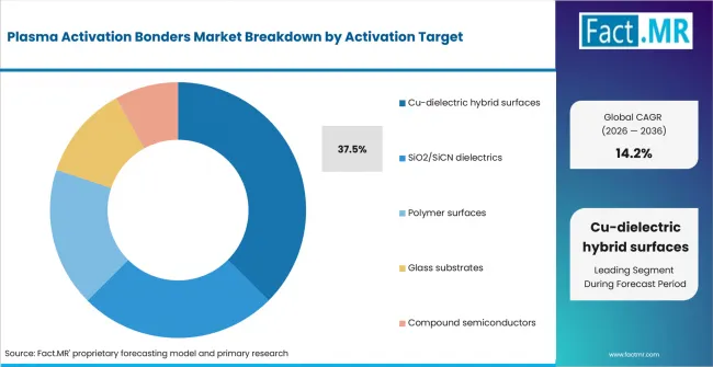
Plasma Activation Bonders Market Analysis By Activation Target | Source: Fact.MR
Copper-dielectric hybrid surfaces require simultaneous management of metal oxide, dielectric hydrophilicity and surface contamination. The mixed interface therefore creates more process value for a tightly controlled plasma recipe than a dielectric-only target. SiO2 or SiCN surfaces remain important, but their activation problem is less coupled to copper oxidation and electrical contact resistance. Remote-plasma activation is gaining for hybrid bonding because it avoids ion bombardment that roughens the <0.5 nm-roughness surfaces hybrid bonding requires (EVG presentation lists microroughness <0.5 nm AFM as excellent for bonding). [6] Buyers therefore tend to treat cu-dielectric hybrid surfaces as the practical choice when qualification must balance process capability, repeatability and production economics.
Why does 300 mm lead Wafer Size?
300 mm is projected to account for 42.9% share in 2026.
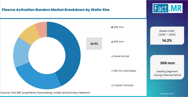
Plasma Activation Bonders Market Analysis By Wafer Size | Source: Fact.MR
The 300 millimeter format aligns with leading logic, memory and advanced-packaging infrastructure, allowing plasma activation to enter production without a separate wafer-size ecosystem. It also spreads uniformity requirements over the largest mainstream wafer area. The 200 millimeter market is substantial in specialty devices, but the strongest hybrid-bonding capital intensity sits in 300 millimeter fabs. After activation and alignment, the bond-front progresses rapidly across the entire wafer at room temperature, followed by ~350 °C anneal converting dielectric hydrogen bonds to covalent bonds while copper fuses (Semiconductor Engineering). [4] Buyers therefore tend to treat 300 mm as the practical choice when qualification must balance process capability, repeatability and production economics.
Why do Foundries lead End User?
Foundries are projected to account for 28.6% share in 2026.
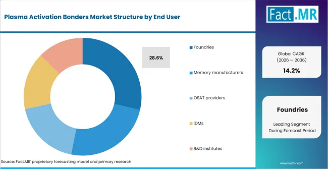
Plasma Activation Bonders Market Analysis By End User | Source: Fact.MR
Foundries must qualify activation across multiple dielectric stacks, copper schemes and customer designs, making recipe flexibility and chamber matching central purchase criteria. The same platform can support logic chiplets, image sensors and other heterogeneous flows. Memory manufacturers can drive very high volumes, but their process mix is narrower and more architecture-specific. Plasma exposure creates reactive dangling bonds and silanol (-OH) groups on Si/dielectric surfaces, making them strongly hydrophilic; van der Waals bonds form on contact and convert to covalent Si-O-Si bridges during low-temperature anneal - avoiding the >600 °C budgets that would destroy pre-processed CMOS. [1] Buyers therefore tend to treat foundries as the practical choice when qualification must balance process capability, repeatability and production economics.
What is accelerating Plasma Activation Bonders Market adoption, and what is holding it back?
The strongest accelerator is mechanism, while the main restraint is that over-activation can damage polymers or alter dielectric surfaces, while under-activation leaves weak or non-uniform bonds.
Drivers Impact Analysis
| DRIVER | (~) % IMPACT ON CAGR | GEOGRAPHIC RELEVANCE | IMPACT TIMELINE |
|---|---|---|---|
| Mechanism | +4.0% | Global leading-edge fabs | Medium term (2-4 years) |
| Two equipment families | +3.3% | Global leading-edge fabs | Medium term (2-4 years) |
| Dielectric-specific chemistry | +2.7% | Global leading-edge fabs | Medium term (2-4 years) |
| Hybrid bonding flow context | +2.1% | Global leading-edge fabs | Medium term (2-4 years) |
Source: Fact.MR analysis. Updated Jul 22, 2026
- Mechanism: Plasma exposure creates reactive dangling bonds and silanol (-OH) groups on Si/dielectric surfaces, making them strongly hydrophilic; van der Waals bonds form on contact and convert to covalent Si-O-Si bridges during low-temperature anneal - avoiding the >600 °C budgets that would destroy pre-processed CMOS. [1][2]
- Two equipment families: Atmospheric-pressure PAB (dielectric barrier discharge, corona, plasma jet; ~40 s treatment, synthetic air or O2 for Si; Ar/H2 or humid O2 for glass/LiTaO3) vs. low-pressure PAB (RIE/ICP-RIE/remote plasma at 0.1-100 Pa, 13.56 MHz, 30-60 s). [2]
- Dielectric-specific chemistry: For SiCN/SiO hybrid-bonding dielectrics, O2 and N2 capacitively-coupled plasma treatments (dual-RF, HF for generation + LF for ion acceleration) keep RMS roughness within 0.1 nm while tuning bonding energy; measured by double-cantilever-beam after 350 °C/1 h batch anneal (Sungkyunkwan University process study). [3]
- Hybrid bonding flow context: After activation and alignment, the bond-front progresses rapidly across the entire wafer at room temperature, followed by ~350 °C anneal converting dielectric hydrogen bonds to covalent bonds while copper fuses (Semiconductor Engineering). [4]
Opportunity Impact Analysis
| OPPORTUNITY | (~) % IMPACT ON CAGR | GEOGRAPHIC RELEVANCE | IMPACT TIMELINE |
|---|---|---|---|
| Activation bonded into the cluster | +2.4% | Global leading-edge fabs | Medium term (2-4 years) |
| Damage-free remote plasma | +1.8% | Global leading-edge fabs | Medium term (2-4 years) |
| Compound-semiconductor and heterogeneous bonding | +1.4% | Global leading-edge fabs | Medium term (2-4 years) |
Source: Fact.MR analysis. Updated Jul 22, 2026
- Activation bonded into the cluster: The clear trend is from standalone activation tools to integrated activate to rinse to dry to bond chains (single-digit-minute queue times), driven by the surface-decay physics above.
- Damage-free remote plasma: Remote-plasma activation is gaining for hybrid bonding because it avoids ion bombardment that roughens the <0.5 nm-roughness surfaces hybrid bonding requires (EVG presentation lists microroughness <0.5 nm AFM as excellent for bonding). [6]
- Compound-semiconductor and heterogeneous bonding: Plasma activation is the enabling step for III-V-on-insulator, GeOI, InP/InGaAs-to-Si bonding for electronic-photonic ICs (University of Tokyo's Takagi/Takenaka lab adopted EVG810LT for this). [7]
Restraints Impact Analysis
| RESTRAINT | (~) % IMPACT ON CAGR | GEOGRAPHIC RELEVANCE | IMPACT TIMELINE |
|---|---|---|---|
| Primary qualification constraint | -2.1% | Global leading-edge fabs | Medium term (2-4 years) |
| Buried-defect escape | -1.7% | Global leading-edge fabs | Medium term (2-4 years) |
Source: Fact.MR analysis. Updated Jul 22, 2026
- Primary qualification constraint: Over-activation can damage polymers or alter dielectric surfaces, while under-activation leaves weak or non-uniform bonds. [1][2]
- Buried-defect escape: Plasma exposure creates reactive dangling bonds and silanol (-OH) groups on Si/dielectric surfaces, making them strongly hydrophilic; van der Waals bonds form on contact and convert to covalent Si-O-Si bridges during low-temperature anneal - avoiding the >600 °C budgets that would destroy pre-processed CMOS. [1][2]
- Buried-defect escape: Remote plasma avoids ion-bombardment damage. [2]
Which countries are scaling Plasma Activation Bonders Market fastest?
For Plasma Activation Bonders Market, South Korea's 15.0% CAGR reflects high-volume memory, HBM and vertically integrated semiconductor manufacturing.
- Countries differ less by the headline CAGR than by the type of semiconductor work creating demand for the Plasma Activation Bonders Market.
- Vietnam takes a different path through expanding back-end assembly and electronics manufacturing capacity.
- Taiwan and Malaysia remain aligned through distinct combinations of device production, equipment development and advanced packaging investment.
- South Korea develops through high-volume memory, HBM and vertically integrated semiconductor manufacturing, while Singapore relies on advanced-packaging R&D, specialty fabs and regional assembly and test operations.
- Markets with similar CAGRs can follow different development paths because installed fabs, device mix, local equipment capability, export controls and qualification cycles differ.
The full report compares the six named country markets within the wider regional coverage of North America, Latin America, Europe, East Asia, South Asia & Oceania, and the Middle East & Africa.
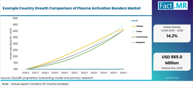
Example Country Growth Comparison Of Plasma Activation Bonders Market | Source: Fact.MR
| COUNTRY | CAGR, 2026 to 2036 |
|---|---|
| Vietnam | 15.8% |
| Taiwan | 15.4% |
| Malaysia | 15.1% |
| South Korea | 15.0% |
| Singapore | 14.4% |
Source: Fact.MR analysis. Updated Jul 22, 2026
What is driving Vietnam's growth through 2036?
15.8% CAGR, supported by expanding back-end assembly and electronics manufacturing capacity.
Vietnam combines expanding back-end assembly and electronics manufacturing capacity with a 8.1% share of 2026 demand across the six profiled countries. Remote-plasma activation is gaining for hybrid bonding because it avoids ion bombardment that roughens the <0.5 nm-roughness surfaces hybrid bonding requires (EVG presentation lists microroughness <0.5 nm AFM as excellent for bonding). [6] The commercial link is the need to solve the problem of creating highly reactive hydrophilic surfaces without plasma damage, particles or an uncontrolled delay before contact as capacity and process complexity increase.
What is driving Taiwan's growth through 2036?
15.4% CAGR, supported by leading foundry production, advanced packaging and a dense OSAT and substrate supply chain.
Taiwan combines leading foundry production, advanced packaging and a dense OSAT and substrate supply chain with a 25.0% share of 2026 demand across the six profiled countries. Plasma activation is the enabling step for III-V-on-insulator, GeOI, InP/InGaAs-to-Si bonding for electronic-photonic ICs (University of Tokyo's Takagi/Takenaka lab adopted EVG810LT for this). [7] The commercial link is the need to solve the problem of creating highly reactive hydrophilic surfaces without plasma damage, particles or an uncontrolled delay before contact as capacity and process complexity increase.
What is driving Malaysia's growth through 2036?
15.1% CAGR, supported by large-scale outsourced assembly, test and package manufacturing.
Malaysia combines large-scale outsourced assembly, test and package manufacturing with a 15.1% share of 2026 demand across the six profiled countries.
What is driving South Korea's growth through 2036?
15.0% CAGR, supported by high-volume memory, HBM and vertically integrated semiconductor manufacturing.
Sungkyunkwan University-led published work on SiCN/SiO plasma activation directly supports Samsung/SK hynix hybrid-bond adoption for HBM and NAND. This environment creates a clear qualification pathway for the Plasma Activation Bonders Market because buyers must solve the problem of creating highly reactive hydrophilic surfaces without plasma damage, particles or an uncontrolled delay before contact at production scale.
What is driving Singapore's growth through 2036?
14.4% CAGR, supported by advanced-packaging R&D, specialty fabs and regional assembly and test operations.
Singapore combines advanced-packaging R&D, specialty fabs and regional assembly and test operations with a 11.5% share of 2026 demand across the six profiled countries. Atmospheric-pressure PAB (dielectric barrier discharge, corona, plasma jet; ~40 s treatment, synthetic air or O2 for Si; Ar/H2 or humid O2 for glass/LiTaO3) vs. [2] The commercial link is the need to solve the problem of creating highly reactive hydrophilic surfaces without plasma damage, particles or an uncontrolled delay before contact as capacity and process complexity increase.
Who leads the Plasma Activation Bonders Market?
EV Group and SUSS MicroTec lead the competitive landscape, followed by Applied Materials and Lam Research as the next tier of challengers.
EV Group participates through wafer bonding, activation and cluster-integrated process control. EVG810LT orders for compound-semiconductor research; SmartView + activation integration; published process windows (bond chamber variables: time, temperature, force, atmosphere, UV energy, plasma). [7][6] SUSS MicroTec participates through wafer alignment, bonding and advanced-packaging lithography. Particle control, mini-environments, stability and CMP-interface specs (up to 5 nm Cu dishing) that define what the activated surface must look like at bond. Applied Materials participates through deposition, etch, materials engineering and integrated process modules, with relevance determined by its ability to address the challenge of creating highly reactive hydrophilic surfaces without plasma damage, particles or an uncontrolled delay before contact. Lam Research participates through etch, deposition, clean and advanced memory process integration, with relevance determined by its ability to address the challenge of creating highly reactive hydrophilic surfaces without plasma damage, particles or an uncontrolled delay before contact.
Nordson MARCH holds a more specialized role through plasma treatment and surface activation, particularly where custom integration and service coverage affect qualification. PVA TePla holds a more specialized role through plasma systems and materials processing, particularly where custom integration and service coverage affect qualification.
Competition is expected to center on repeatable process performance, integration with adjacent modules, installed-base service and documented capability to address the challenge of creating highly reactive hydrophilic surfaces without plasma damage, particles or an uncontrolled delay before contact. Buyers are likely to compare accuracy, defect prevention, throughput, recipe stability and the completeness of the delivered process cell.
Which companies are the key providers?
Key companies include EV Group; SUSS MicroTec; Applied Materials; Lam Research; Nordson MARCH; PVA TePla.
- EV Group
- SUSS MicroTec
- Applied Materials
- Lam Research
- Nordson MARCH
- PVA TePla
Bibliography
- [1] Keylinktech. (n.d.). Plasma Surface Activation For Wafer Bonding And Mems Manufacturing.
- [2] En. (n.d.). Plasma Activated Bonding.
- [3] Swb. (n.d.). 2020 14.
- [4] Semiconductor Engineering. (n.d.). Making Hybrid Bonding Better.
- [6] EV Group. (n.d.). Ev Group Installs Low Temperature Plasma Activation System For Compound Semiconductor Research At The University Of Tokyo.
- [7] Patsnap. (n.d.). Hybrid Bonding In 3D Ic Packaging Cu To Cu Explained.
This Report Addresses
- The report provides strategic intelligence on Plasma Activation Bonders Market across Plasma Source and Integration Mode choices that shape purchasing decisions.
- Segment analysis covers N2 remote plasma as the share leader within the 2026 market structure.
- Regional outlook evaluates Taiwan alongside South Korea and Malaysia, while Singapore and Vietnam complete the growth comparison.
- Competitive analysis profiles EV Group and SUSS MicroTec alongside Applied Materials and Lam Research, followed by additional active providers.
- Use-case assessment covers the categories and applications that shape demand in the Plasma Activation Bonders Market across the forecast period.
What does the Plasma Activation Bonders Market cover?
The market covers equipment and process systems configured to address the challenge of creating highly reactive hydrophilic surfaces without plasma damage, particles or an uncontrolled delay before contact.
Plasma activation bonders are wafer/die bonding systems whose front-end module activates the bonding surface with plasma (N2, O2, Ar/H2, remote or direct, low-pressure or atmospheric) to raise surface energy, enabling direct/fusion or hybrid bonds at anneal temperatures below ~400 °C. The market spans standalone activation systems (e.g., EVG810LT) and activation modules integrated into fusion/hybrid bond clusters.
Commercial value arises from the complete configured system, including process control, handling, software and integrated modules required for repeatable operation. Finished semiconductor devices, package value and unrelated parent-market equipment are excluded.
What is included in the scope?
The scope includes systems used by foundries and the other end-user groups listed in the segmentation.
The market is segmented by Plasma Source, including N2 remote plasma, O2 plasma, Ar plasma, H2/forming gas plasma, Mixed-chemistry plasma; Integration Mode, including Cluster-integrated activation, Standalone activation modules, Inline track-integrated, Batch activation chambers, Atmospheric plasma units; Activation Target, including Cu-dielectric hybrid surfaces, SiO2/SiCN dielectrics, Polymer surfaces, Glass substrates, Compound semiconductors; Wafer Size, including 300 mm, 200 mm, Panel format, 150 mm and below, Custom formats; End User, including Foundries, Memory manufacturers, OSAT providers, IDMs, R&D institutes.
Integrated handling, metrology, cleaning, activation, process-control or support modules are included when delivered as part of the configured market system.
What is excluded from the scope?
The scope excludes unrelated semiconductor equipment, standalone materials and components sold independently of the configured system.
It also excludes facility construction, cleanroom infrastructure, the value of processed wafers or packages, and adjacent process steps that are not part of the defined equipment category.
How Was the Analysis Built?
Fact.MR is of the opinion that this assessment combines structured market analysis with a review of public information and industry evidence relevant to the market.
- Market Assessment: The analysis considers demand patterns, supply conditions, segment mix, country activity, company participation, and adoption trends.
- Evidence Review: Public company disclosures, government and regulatory publications, trade information, technical literature, and industry records inform the assessment.
- Validation and Updates: Findings are cross-checked against available market indicators and reviewed when material market developments emerge.
Segmentation
What is the report's scope and coverage?
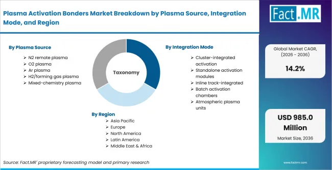
Plasma Activation Bonders Market Breakdown By Plasma Source, Integration Mode, And Region | Source: Fact.MR
| Attribute | Details |
|---|---|
| Quantitative Units | USD 262.0 million in 2026 to USD 985.0 million by 2036 at a 14.2% CAGR |
| Market Definition | Plasma activation bonders are wafer/die bonding systems whose front-end module activates the bonding surface with plasma (N2, O2, Ar/H2, remote or direct, low-pressure or atmospheric) to raise surface energy, enabling direct/fusion or hybrid bonds at anneal temperatures below ~400 °C. The market spans standalone activation systems (e.g., EVG810LT) and activation modules integrated into fusion/hybrid bond clusters. |
| Plasma Source | N2 remote plasma; O2 plasma; Ar plasma; H2/forming gas plasma; Mixed-chemistry plasma |
| Integration Mode | Cluster-integrated activation; Standalone activation modules; Inline track-integrated; Batch activation chambers; Atmospheric plasma units |
| Activation Target | Cu-dielectric hybrid surfaces; SiO2/SiCN dielectrics; Polymer surfaces; Glass substrates; Compound semiconductors |
| Wafer Size | 300 mm; 200 mm; Panel format; 150 mm and below; Custom formats |
| End User | Foundries; Memory manufacturers; OSAT providers; IDMs; R&D institutes |
| Regions Covered | North America; Latin America; Europe; East Asia; South Asia & Oceania; Middle East & Africa |
| Countries Covered | Taiwan; South Korea; Malaysia; Singapore; Vietnam |
| Key Companies Profiled | EV Group; SUSS MicroTec; Applied Materials; Lam Research; Nordson MARCH; PVA TePla |
| Forecast Period | 2026 to 2036 |
| Approach | Hybrid top-down and bottom-up approach using demand indicators across Plasma Source; Integration Mode; Activation Target; Wafer Size; End User; country-level growth; company participation and adoption trends |
Source: Fact.MR analysis. Updated Jul 22, 2026
How is the market segmented?
-
By Plasma Source
- N2 remote plasma
- O2 plasma
- Ar plasma
- H2/forming gas plasma
- Mixed-chemistry plasma
-
By Integration Mode
- Cluster-integrated activation
- Standalone activation modules
- Inline track-integrated
- Batch activation chambers
- Atmospheric plasma units
-
By Activation Target
- Cu-dielectric hybrid surfaces
- SiO2/SiCN dielectrics
- Polymer surfaces
- Glass substrates
- Compound semiconductors
-
By Wafer Size
- 300 mm
- 200 mm
- Panel format
- 150 mm and below
- Custom formats
-
By End User
- Foundries
- Memory manufacturers
- OSAT providers
- IDMs
- R&D institutes
-
By Region
- North America
- Other regional markets assessed at aggregate level
- Latin America
- Other regional markets assessed at aggregate level
- Europe
- Other regional markets assessed at aggregate level
- East Asia
- Taiwan
- South Korea
- South Asia & Oceania
- Malaysia
- Singapore
- Vietnam
- Middle East & Africa
- Other regional markets assessed at aggregate level
- North America
Frequently Asked Questions
Which Plasma Source leads the Plasma Activation Bonders Market?
Which Integration Mode leads the Plasma Activation Bonders Market?
Which Activation Target leads the Plasma Activation Bonders Market?
Which Wafer Size leads the Plasma Activation Bonders Market?
Which End User leads the Plasma Activation Bonders Market?
What CAGR is projected for Vietnam in the Plasma Activation Bonders Market?
What CAGR is projected for Taiwan in the Plasma Activation Bonders Market?
What CAGR is projected for Malaysia in the Plasma Activation Bonders Market?
What CAGR is projected for South Korea in the Plasma Activation Bonders Market?
What CAGR is projected for Singapore in the Plasma Activation Bonders Market?
What is the primary driver of the Plasma Activation Bonders Market?
What is the main restraint in the Plasma Activation Bonders Market?
Who worked on this report


Preview the report firsthand - request a free sample
Free SampleGet the brochure for pricing and purchase details
Download PDF