- Market Value (2025): USD 357.1 Mn
- Estimated Value (2026): USD 405.0 Mn
- Forecast Value (2036): USD 1420.0 Mn
- CAGR (2026-2036): 13.4%
What is the Void-Free Epi Tools Market forecast to be worth by 2036?
USD 405.0 million in 2026 to USD 1,420.0 million by 2036, at a 13.4% CAGR.
- The Void-Free Epi Tools Market crossed a valuation of USD 357.1 million in 2025, supported by demand from Foundries serving SiGe workflows that require initiating selective epitaxy uniformly inside confined recesses without oxide remnants, seam voids or crystal defects.
- Demand is projected to increase from USD 405.0 million in 2026 to USD 1,420.0 million by 2036.
- The market is forecast to record a 13.4% CAGR from 2026 to 2036 as why voids form and why they matter, toolmaker requirement language and integration sequence dependence remain central purchase reasons.
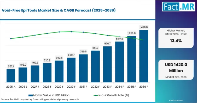
Void Free Epi Tools Market Value Analysis | Source: Fact.MR
What are the defining numbers behind Void-Free Epi Tools Market growth?
USD 1,015.0 million absolute opportunity is expected by 2036.
- Demand Drivers in the Market
- Why voids form and why they matter: Demand for defect-control-focused epi tools traces to a specific failure mechanism: selective epi grows from exposed crystalline surfaces, and poor nucleation at the recess bottom, from residual oxide, carbon contamination, or wrong facet initiation, leaves interfacial voids that raise source/drain resistance and kill strain transfer, giving buyers a direct line from tool capability to device performance.
- Toolmaker requirement language: Toolmakers are naming defect-free epi as an explicit spec rather than a nicety: TEL's GAA module list states directly that SiGe/Si must be defect-free, uniform epitaxy for the mold stack, backed by highly selective SiGe etch and collapse-free drying downstream, making void-free performance an equipment-defined requirement buyers can hold vendors to.
- Integration sequence dependence: Void-free source/drain epi outcomes depend on process steps upstream of the epi chamber itself: any inner-spacer residue or recess-etch roughness seeds voids in the selectively formed n-type or p-type source/drain layers, which is why preventing oxidation of the Si/SiGe trench and loading-free recess etch are named as TEL module requirements feeding directly into epi quality.
- In-situ doping without defects: Demand for tightly controlled in-situ doping is rising as devices push boron concentrations in SiGe stressors to 1-3x10^20 per cubic centimeter and adopt delta-layer doping schemes, both of which must be incorporated without precipitates, a reactor chemistry and temperature-window problem that keeps epi tool control specs tightening alongside doping targets.
- Key Segments Analyzed
- By Defect Control Method: In-situ pre-clean is projected to hold 31.0% share in 2026, supported by a clear process advantage: In-situ pre-clean removes native oxide and adsorbed contamination immediately before growth, allowing nucleation to begin uniformly across the recessed surface. It attacks the defect source before deposition rather than trying to close a void later.
- By Feature Geometry: Confined nanosheet gaps are projected to hold 42.4% share in 2026, supported by a clear process advantage: Confined nanosheet gaps restrict precursor transport and create competing growth fronts that can close around a seam or void. They therefore place the strongest value on flow design, nucleation control and cyclic growth strategies.
- By Material System: SiGe is projected to hold 41.6% share in 2026, supported by a clear process advantage: SiGe supports selective source-drain and channel-stack engineering but is highly sensitive to surface preparation, germanium composition and facet evolution. Those sensitivities make defect-control capability commercially visible.
- By Defect Target: Void elimination is projected to hold 39.1% share in 2026, supported by a clear process advantage: Void elimination is the defining outcome because an enclosed gap becomes a high-resistance region, a stress concentrator or a source of later device variability. It can remain hidden even when the top surface appears fully filled.
- By End User: Foundries are projected to hold 32.4% share in 2026, supported by a clear process advantage: Foundries need void-free selective epitaxy across different layouts and design densities, making pattern loading and across-wafer repeatability central to qualification. A robust tool reduces the amount of design-specific process retuning.
- Analyst Opinion at Fact.MR
- Shambhu Nath Jha, Sr. Consultant at Fact.MR, states, 'Buyers should evaluate the complete process sequence around initiating selective epitaxy uniformly inside confined recesses without oxide remnants, seam voids or crystal defects. Technical review should focus on repeatability, integration, defect control and production throughput rather than a single headline specification. Suppliers that connect tool performance to measurable yield and qualification results are likely to build trust faster.'
- Strategic Implications
- Qualification should measure void probability and electrical impact across recess geometry, beyond blanket-film growth rate.
- Equipment suppliers should document how their systems address the challenge of initiating selective epitaxy uniformly inside confined recesses without oxide remnants, seam voids or crystal defects across production-representative wafers, panels, dies or packages.
- Procurement teams should compare defect-free epitaxial coverage, interface quality, precursor purity, reactor conditioning, wafer throughput and process-window stability for the target device stack.
Taiwan is projected to record a 15.0% CAGR as leading foundry production, advanced packaging and a dense OSAT and substrate supply chain supports relevant capital spending; South Korea is projected to record a 14.4% CAGR as high-volume memory, HBM and vertically integrated semiconductor manufacturing supports relevant capital spending; USA is projected to record a 14.9% CAGR as leading-edge logic, high-performance computing, federally supported semiconductor R&D and a large domestic equipment base supports relevant capital spending; Japan is projected to record a 14.0% CAGR as semiconductor equipment, materials, inspection and memory-process expertise supports relevant capital spending; while Germany is projected to record a 12.8% CAGR as precision equipment, materials engineering and automotive and power-semiconductor demand supports relevant capital spending through 2036.
How does the Void-Free Epi Tools Market break down by segment?
In-situ pre-clean leads Defect Control Method with a 31.0% share, while Confined nanosheet gaps accounts for 42.4% of Feature Geometry in 2026.
Why does In-situ pre-clean lead Defect Control Method?
In-situ pre-clean is projected to account for 31.0% share in 2026.
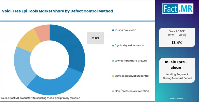
Void Free Epi Tools Market Analysis By Defect Control Method | Source: Fact.MR
In-situ pre-clean removes native oxide and adsorbed contamination immediately before growth, allowing nucleation to begin uniformly across the recessed surface. It attacks the defect source before deposition rather than trying to close a void later. Cyclic deposition-etch can heal profile problems during growth, but it cannot fully compensate for a contaminated or non-nucleating starting surface. Integrated clean (low-temp H2 bake, radical/remote-plasma preclean) inside the epi reactor to strip native oxide without thermal budget - the primary void-elimination lever. Buyers therefore tend to treat in-situ pre-clean as the practical choice when qualification must balance process capability, repeatability and production economics.
Why do Confined nanosheet gaps lead Feature Geometry?
Confined nanosheet gaps are projected to account for 42.4% share in 2026.
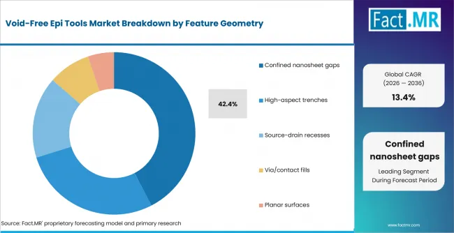
Void Free Epi Tools Market Analysis By Feature Geometry | Source: Fact.MR
Confined nanosheet gaps restrict precursor transport and create competing growth fronts that can close around a seam or void. They therefore place the strongest value on flow design, nucleation control and cyclic growth strategies. High-aspect trenches are also transport limited, but their open top and larger volume can provide a less constrained growth path. Multi-step pressure/temperature/gas-ratio ramps that control (111) vs (100) facet propagation to avoid seams at coalescence in narrow trenches (nanosheet S/D geometry). Buyers therefore tend to treat confined nanosheet gaps as the practical choice when qualification must balance process capability, repeatability and production economics.
Why does SiGe lead Material System?
SiGe is projected to account for 41.6% share in 2026.
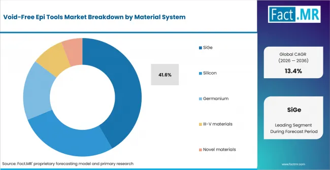
Void Free Epi Tools Market Analysis By Material System | Source: Fact.MR
SiGe supports selective source-drain and channel-stack engineering but is highly sensitive to surface preparation, germanium composition and facet evolution. Those sensitivities make defect-control capability commercially visible. Silicon growth has a broader process base and generally a wider integration window, reducing the incremental value of specialized void-control features. TEL's GAA module list names the spec directly: SiGe/Si: Defect free, Uniform EPI for the mold stack; with highly selective SiGe etch and collapse-free drying downstream. Defect-free epi is the equipment-defined requirement, not a materials nicety. Buyers therefore tend to treat siGe as the practical choice when qualification must balance process capability, repeatability and production economics.
Why does Void elimination lead Defect Target?
Void elimination is projected to account for 39.1% share in 2026.
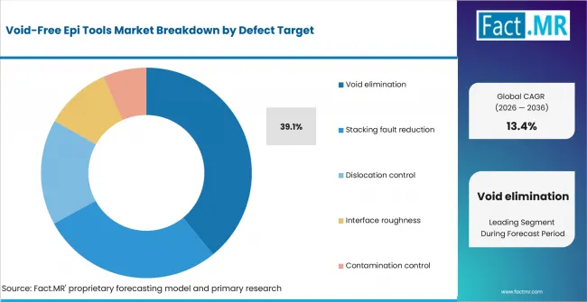
Void Free Epi Tools Market Analysis By Defect Target | Source: Fact.MR
Void elimination leads this segment because trapped gaps inside recessed features weaken electrical performance and reduce process yield. The main focus is to achieve uniform nucleation and complete material fill from the bottom and sidewalls without leaving empty spaces. Methods such as in-situ pre-clean, selective growth, and cyclic deposition-etch help control the profile before a void forms. Other defect targets, including seams and surface roughness, remain important, but internal voids create a more direct risk to device reliability. This makes void elimination the main qualification target when manufacturers compare process control, repeatability, and production cost.
Why do Foundries lead End User?
Foundries are projected to account for 32.4% share in 2026.
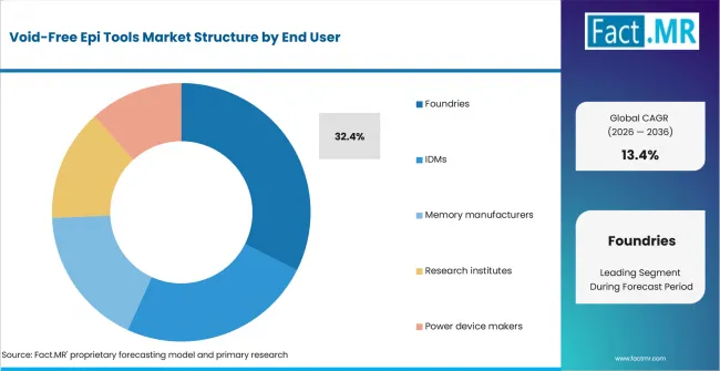
Void Free Epi Tools Market Analysis By End User | Source: Fact.MR
Foundries need void-free selective epitaxy across different layouts and design densities, making pattern loading and across-wafer repeatability central to qualification. A robust tool reduces the amount of design-specific process retuning. IDMs can restrict the geometry set more tightly, while foundries must support a broader customer pattern space. Boron at 1-3×10²⁰ cm⁻³ in SiGe stressors (CAS 2017 study data) and delta-layer doping schemes (GlobalFoundries SG 2015 patents) must be incorporated without precipitates - a reactor chemistry/temperature-window problem. Buyers therefore tend to treat foundries as the practical choice when qualification must balance process capability, repeatability and production economics.
What is accelerating Void-Free Epi Tools Market adoption, and what is holding it back?
The strongest accelerator is why voids form and why they matter, while the main restraint is that nucleation sensitivity to surface preparation and facet geometry makes the process difficult to transfer across device layouts.
Drivers Impact Analysis
| DRIVER | (~) % IMPACT ON CAGR | GEOGRAPHIC RELEVANCE | IMPACT TIMELINE |
|---|---|---|---|
| Why voids form and why they matter | +3.8% | Global leading-edge fabs | Medium term (2-4 years) |
| Toolmaker requirement language | +3.1% | Global leading-edge fabs | Medium term (2-4 years) |
| Integration sequence dependence | +2.5% | Global leading-edge fabs | Medium term (2-4 years) |
| In-situ doping without defects | +2.0% | Global leading-edge fabs | Medium term (2-4 years) |
Source: Fact.MR analysis. Updated Jul 23, 2026
- Why voids form and why they matter: Selective epi grows from exposed crystalline surfaces; poor nucleation at the recess bottom (residual oxide, carbon contamination, wrong facet initiation) leaves interfacial voids that raise S/D resistance and kill strain transfer.
- Toolmaker requirement language: TEL's GAA module list names the spec directly: SiGe/Si: Defect free, Uniform EPI for the mold stack; with highly selective SiGe etch and collapse-free drying downstream. Defect-free epi is the equipment-defined requirement, not a materials nicety.
- Integration sequence dependence: Void-free S/D epi depends on upstream inner-spacer and recess-etch quality: n-type or p-type source/drain epitaxial layers are selectively formed on either sides of the exposed nanosheet ends - any inner-spacer residue or recess roughness seeds voids. Preventing oxidation of the Si/SiGe trench and loading-free recess etch are named TEL module requirements feeding epi quality.
- In-situ doping without defects: Boron at 1-3×10²⁰ cm⁻³ in SiGe stressors (CAS 2017 study data) and delta-layer doping schemes (GlobalFoundries SG 2015 patents) must be incorporated without precipitates - a reactor chemistry/temperature-window problem.
Opportunity Impact Analysis
| OPPORTUNITY | (~) % IMPACT ON CAGR | GEOGRAPHIC RELEVANCE | IMPACT TIMELINE |
|---|---|---|---|
| Pre-epi surface engineering in-situ | +2.3% | Global leading-edge fabs | Medium term (2-4 years) |
| Facet-controlled growth recipes | +1.7% | Global leading-edge fabs | Medium term (2-4 years) |
| Ge and III-V extensions | +1.3% | Global leading-edge fabs | Medium term (2-4 years) |
Source: Fact.MR analysis. Updated Jul 23, 2026
- Pre-epi surface engineering in-situ: Integrated clean (low-temp H2 bake, radical/remote-plasma preclean) inside the epi reactor to strip native oxide without thermal budget - the primary void-elimination lever.
- Facet-controlled growth recipes: Multi-step pressure/temperature/gas-ratio ramps that control (111) vs (100) facet propagation to avoid seams at coalescence in narrow trenches (nanosheet S/D geometry).
- Ge and III-V extensions: Selective in-situ-doped SiGe on bulk Ge demonstrated for p+/n junctions (KTH 2020) - void-free nucleation on non-Si surfaces is the next capability differentiator.
Restraints Impact Analysis
| RESTRAINT | (~) % IMPACT ON CAGR | GEOGRAPHIC RELEVANCE | IMPACT TIMELINE |
|---|---|---|---|
| Primary qualification constraint | -2.0% | Global leading-edge fabs | Medium term (2-4 years) |
| Surface-state degradation | -1.6% | Global leading-edge fabs | Medium term (2-4 years) |
Source: Fact.MR analysis. Updated Jul 23, 2026
- Primary qualification constraint: Nucleation sensitivity to surface preparation and facet geometry makes the process difficult to transfer across device layouts.
- Surface-state degradation: Void-free S/D epi depends on upstream inner-spacer and recess-etch quality: n-type or p-type source/drain epitaxial layers are selectively formed on either sides of the exposed nanosheet ends - any inner-spacer residue or recess roughness seeds voids. Preventing oxidation of the Si/SiGe trench and loading-free recess etch are named TEL module requirements feeding epi quality.
Which countries are scaling Void-Free Epi Tools Market fastest?
For Void Free Epi Tools Market, South Korea's 14.4% CAGR reflects high-volume memory, HBM and vertically integrated semiconductor manufacturing.
- Countries differ less by the headline CAGR than by the type of semiconductor work creating demand for the Void-Free Epi Tools Market.
- Taiwan demand is associated with foundry-led epitaxy qualification and advanced packaging supply links, while USA demand reflects logic-node development, domestic equipment capability and substrate R&D.
- South Korea remains aligned through distinct combinations of device production, equipment development and advanced packaging investment.
- Japan develops through semiconductor equipment, materials, inspection and memory-process expertise, while Germany relies on precision equipment, materials engineering and automotive and power-semiconductor demand.
- Growth patterns depend on epitaxy adoption at advanced nodes, material sourcing, reactor availability, local fab investment and qualification timing.
The full report compares the named country markets within the wider regional coverage of North America, Latin America, Europe, East Asia, South Asia & Oceania, and the Middle East & Africa.
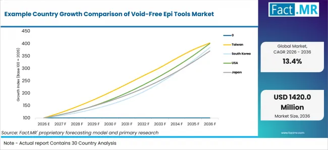
Example Country Growth Comparison Of Void Free Epi Tools Market | Source: Fact.MR
| COUNTRY | CAGR, 2026 to 2036 |
|---|---|
| Taiwan | 15.0% |
| USA | 14.9% |
| South Korea | 14.4% |
| Japan | 14.0% |
| Germany | 12.8% |
Source: Fact.MR analysis. Updated Jul 23, 2026
What is driving Taiwan's growth through 2036?
15.0% CAGR, shaped by Taiwan's foundry process ramps, epitaxy qualification requirements and local packaging ecosystem.
Samsung/TSMC qualification lines set the defect-density specs vendors must meet. This environment creates a clear qualification pathway for the Void-Free Epi Tools Market because buyers must solve the problem of initiating selective epitaxy uniformly inside confined recesses without oxide remnants, seam voids or crystal defects at production scale.
What is driving USA's growth through 2036?
14.9% CAGR, supported by leading-edge logic, high-performance computing, federally supported semiconductor R&D and a large domestic equipment base.
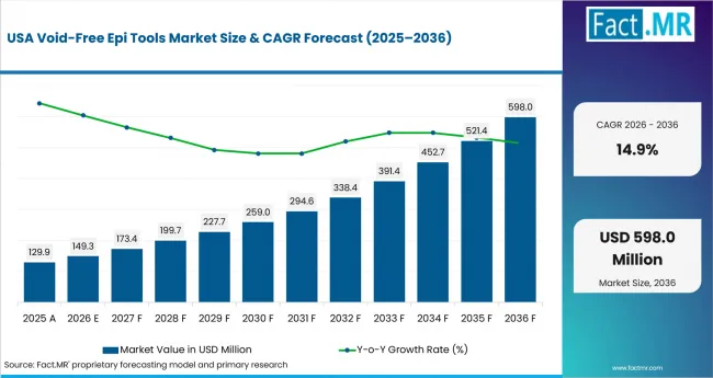
Void Free Epi Tools Market Country Value Analysis | Source: Fact.MR
Applied Materials (integrated epi + preclean); IBM Albany patents on dislocation-free pseudomorphic growth. This environment creates a clear qualification pathway for the Void-Free Epi Tools Market because buyers must solve the problem of initiating selective epitaxy uniformly inside confined recesses without oxide remnants, seam voids or crystal defects at production scale.
What is driving South Korea's growth through 2036?
14.4% CAGR, supported by high-volume memory, HBM and vertically integrated semiconductor manufacturing.
Growth is linked to its large memory-chip production base, rising investment in high-bandwidth memory, and strong control over semiconductor design, and equipment use. Samsung Electronics and SK hynix continue to expand advanced NAND and HBM production, which increases demand for etching systems that maintain deep channel profiles, and high-volume output. This manufacturing strength is expected to keep South Korea among the leading markets for cryogenic NAND etchers.
What is driving Japan's growth through 2036?
14.0% CAGR, supported by semiconductor equipment, materials, inspection and memory-process expertise.
TEL - module-level specs for GAA epi; domestic tool demand from Rapidus 2 nm program. This environment creates a clear qualification pathway for the Void-Free Epi Tools Market because buyers must solve the problem of initiating selective epitaxy uniformly inside confined recesses without oxide remnants, seam voids or crystal defects at production scale.
What is driving Germany's growth through 2036?
12.8% CAGR, supported by precision equipment, materials engineering and automotive and power-semiconductor demand.
Germany combines precision equipment, materials engineering and automotive and power-semiconductor demand with a 3.5% share of 2026 demand across the six profiled countries. TEL's GAA module list names the spec directly: SiGe/Si: Defect free, Uniform EPI for the mold stack; with highly selective Restraints Impact AnalysisSiGe etch and collapse-free drying downstream.The commercial link is the need to solve the problem of initiating selective epitaxy uniformly inside confined recesses without oxide remnants, seam voids or crystal defects as capacity and process complexity increase.
Who leads the Void-Free Epi Tools Market?
Applied Materials and ASM International lead the competitive landscape, followed by Tokyo Electron and Lam Research as the next tier of challengers.
Applied Materials participates through deposition, etch, materials engineering and integrated process modules. Epi with in-situ preclean; GAA module co-optimization. ASM International participates through epitaxy and atomic-layer process equipment. Defect-free SEG for S/D and superlattices; ALD+epi integration. Tokyo Electron participates through etch, clean, deposition and wafer-bonding process equipment. Published defect free, uniform EPI module targets. Lam Research participates through etch, deposition, clean and advanced memory process integration, with relevance determined by its ability to address the challenge of initiating selective epitaxy uniformly inside confined recesses without oxide remnants, seam voids or crystal defects.
Veeco holds a more specialized role through epitaxy and thin-film process equipment, particularly where custom integration and service coverage affect qualification. Nuflare holds a more specialized role through semiconductor process and lithography-related equipment, particularly where custom integration and service coverage affect qualification.
Competition is expected to center on repeatable process performance, integration with adjacent modules, installed-base service and documented capability to address the challenge of initiating selective epitaxy uniformly inside confined recesses without oxide remnants, seam voids or crystal defects. Buyers are likely to compare accuracy, defect prevention, throughput, recipe stability and the completeness of the delivered process cell.
Which companies are the key providers?
Key companies include Applied Materials; ASM International; Tokyo Electron; Lam Research; Veeco; Nuflare.
- Applied Materials
- ASM International
- Tokyo Electron
- Lam Research
- Veeco
- Nuflare
Bibliography
- Applied Materials, Inc. (2025, October 7). Applied Materials unveils next-gen chipmaking products to supercharge AI performance.
- ASM International N.V. (2025). Annual report 2025.
- Tokyo Electron Limited. (2025, February 13). Episode™ 1 single-wafer deposition system for semiconductors: Driving the evolution of AI semiconductors to transform everyday life.
- ASM International N.V. (2025). Built from the atom up: Epitaxy’s defining role in the AI age.
This Report Addresses
- The report provides strategic intelligence on Void-Free Epi Tools Market across Defect Control Method and Feature Geometry choices that shape purchasing decisions.
- Segment analysis covers In-situ pre-clean as the share leader within the 2026 market structure.
- Regional outlook evaluates Taiwan and South Korea alongside USA and Japan, while Germany complete the growth comparison.
- Competitive analysis profiles Applied Materials and ASM International alongside Tokyo Electron and Lam Research, followed by additional active providers.
- Use-case assessment covers the categories and applications that shape demand in the Void-Free Epi Tools Market across the forecast period.
What does the Void-Free Epi Tools Market cover?
The market covers equipment and process systems configured to address the challenge of initiating selective epitaxy uniformly inside confined recesses without oxide remnants, seam voids or crystal defects.
Void-free epi tools are selective epitaxy systems whose core selling point is eliminating voids, seams, and dislocations in grown layers: raised source/drain epi in FinFET/GAA (SiGe:B, Si:P, SiC:P), embedded stressors, and increasingly void-free fill of high-aspect features by epi or epi-like selective deposition. Buyers pay for defect metrics - no interfacial voids at the recess bottom, no stacking faults along faceted growth fronts, no seam where coalescing fronts meet.
Commercial value covers void-free epitaxy reactors, precursor delivery, wafer handling, chamber conditioning, in-situ monitoring and recipe-control software. Finished devices, package value and unrelated semiconductor equipment are excluded.
What is included in the scope?
The scope includes systems used by foundries and the other end-user groups listed in the segmentation.
The market is segmented by Defect Control Method, including In-situ pre-clean, Cyclic deposition-etch, Low-temperature growth, Surface passivation control, Flow/pressure optimization; Feature Geometry, including Confined nanosheet gaps, High-aspect trenches, Source-drain recesses, Via/contact fills, Planar surfaces; Material System, including SiGe, Silicon, Germanium, III-V materials, Novel materials; Defect Target, including Void elimination, Stacking fault reduction, Dislocation control, Interface roughness, Contamination control; End User, including Foundries, IDMs, Memory manufacturers, Research institutes, Power device makers.
Precursor purification, gas delivery, wafer transfer, chamber clean, in-situ monitoring and reactor-control modules are included only when part of the configured epitaxy system.
What is excluded from the scope?
The scope excludes unrelated semiconductor equipment, standalone materials and components sold independently of the configured system.
It also excludes facility construction, cleanroom infrastructure, the value of processed wafers or packages, and adjacent process steps that are not part of the defined equipment category.
How Was the Analysis Built?
Fact.MR is of the opinion that this assessment combines structured market analysis with a review of public information and industry evidence relevant to the market.
- Market Assessment: The analysis considers demand patterns, supply conditions, segment mix, country activity, company participation, and adoption trends.
- Evidence Review: Public company disclosures, government and regulatory publications, trade information, technical literature, and industry records inform the assessment.
- Validation and Updates: Findings are cross-checked against available market indicators and reviewed when material market developments emerge.
Segmentation
What is the report's scope and coverage?
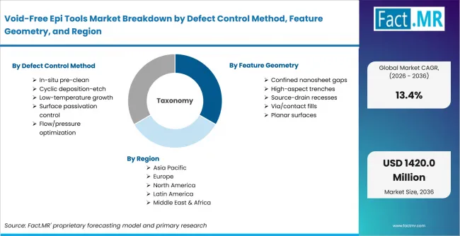
Void Free Epi Tools Market Breakdown By Defect Control Method, Feature Geometry, And Region | Source: Fact.MR
| Attribute | Details |
|---|---|
| Quantitative Units | USD 405.0 million in 2026 to USD 1,420.0 million by 2036 at a 13.4% CAGR |
| Market Definition | Void-free epi tools are selective epitaxy systems whose core selling point is eliminating voids, seams, and dislocations in grown layers: raised source/drain epi in FinFET/GAA (SiGe:B, Si:P, SiC:P), embedded stressors, and increasingly void-free fill of high-aspect features by epi or epi-like selective deposition. Buyers pay for defect metrics - no interfacial voids at the recess bottom, no stacking faults along faceted growth fronts, no seam where coalescing fronts meet. |
| Defect Control Method | In-situ pre-clean; Cyclic deposition-etch; Low-temperature growth; Surface passivation control; Flow/pressure optimization |
| Feature Geometry | Confined nanosheet gaps; High-aspect trenches; Source-drain recesses; Via/contact fills; Planar surfaces |
| Material System | SiGe; Silicon; Germanium; III-V materials; Novel materials |
| Defect Target | Void elimination; Stacking fault reduction; Dislocation control; Interface roughness; Contamination control |
| End User | Foundries; IDMs; Memory manufacturers; Research institutes; Power device makers |
| Regions Covered | North America; Latin America; Europe; East Asia; South Asia & Oceania; Middle East & Africa |
| Countries Covered | Taiwan; South Korea; USA; Japan; Germany |
| Key Companies Profiled | Applied Materials; ASM International; Tokyo Electron; Lam Research; Veeco; Nuflare |
| Forecast Period | 2026 to 2036 |
| Approach | Hybrid top-down and bottom-up approach using demand indicators across Defect Control Method; Feature Geometry; Material System; Defect Target; End User; country-level growth; company participation and adoption trends |
Source: Fact.MR analysis. Updated Jul 23, 2026
How is the market segmented?
-
By Defect Control Method
- In-situ pre-clean
- Cyclic deposition-etch
- Low-temperature growth
- Surface passivation control
- Flow/pressure optimization
-
By Feature Geometry
- Confined nanosheet gaps
- High-aspect trenches
- Source-drain recesses
- Via/contact fills
- Planar surfaces
-
By Material System
- SiGe
- Silicon
- Germanium
- III-V materials
- Novel materials
-
By Defect Target
- Void elimination
- Stacking fault reduction
- Dislocation control
- Interface roughness
- Contamination control
-
By End User
- Foundries
- IDMs
- Memory manufacturers
- Research institutes
- Power device makers
-
By Region
- North America
- USA
- Latin America
- Other regional markets assessed at aggregate level
- Europe
- Germany
- East Asia
-
- Taiwan
- South Korea
- Japan
- South Asia & Oceania
- Other regional markets assessed at aggregate level
- Middle East & Africa
- Other regional markets assessed at aggregate level
- North America
Frequently Asked Questions
Which Defect Control Method leads the Void-Free Epi Tools Market?
Which Feature Geometry leads the Void-Free Epi Tools Market?
Which Material System leads the Void-Free Epi Tools Market?
Which Defect Target leads the Void-Free Epi Tools Market?
Which End User leads the Void-Free Epi Tools Market?
What CAGR is projected for Taiwan in the Void-Free Epi Tools Market?
What CAGR is projected for USA in the Void-Free Epi Tools Market?
What CAGR is projected for South Korea in the Void-Free Epi Tools Market?
What CAGR is projected for Japan in the Void-Free Epi Tools Market?
What CAGR is projected for Germany in the Void-Free Epi Tools Market?
What is the primary driver of the Void-Free Epi Tools Market?
What is the main restraint in the Void-Free Epi Tools Market?
Who worked on this report


Preview the report firsthand - request a free sample
Free SampleGet the brochure for pricing and purchase details
Download PDF