- Market Value (2025): USD 598.4 Mn
- Estimated Value (2026): USD 760.0 Mn
- Forecast Value (2036): USD 8296.0 Mn
- CAGR (2026-2036): 27.0%
What is the Atomic Layer Processors Market forecast to be worth by 2036?
USD 760.0 million in 2026 to USD 8,296.0 million by 2036 at a 27.0% CAGR.
- The atomic layer processors market reached USD 598.4 million in 2025.
- Demand is projected to increase from USD 760.0 million in 2026 to USD 8,296.0 million by 2036.
- The market is forecast to record 27.0% CAGR from 2026 to 2036 as edge AI designers, package engineers and automotive electronics teams adopt tighter atomic-scale process control.
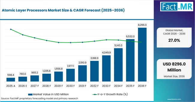
Atomic Layer Processors Market Value Analysis | Source: Fact.MR
What are the defining numbers behind Atomic Layer Processors Market growth?
USD 7,536.0 million absolute opportunity between 2026 and 2036, led by Edge AI, 2.5D packaging and discrete integration.
- Demand Drivers in the Market
- Edge AI processor designers need lower leakage and shorter data paths because local inference places compute close to cameras, lidar and industrial sensors.
- Foundry process teams require scalable 300mm wafer-processing capability to maintain consistent film performance as production volumes increase. SEMI’s Q2 2026 300mm Fab Outlook forecasts global 300mm front-end equipment spending at US$142 billion in 2026, up 25% year over year.
- Advanced packaging engineers need denser processor-to-memory paths. SIA reported in August 2026 that global semiconductor sales reached USD 403.3 billion in the second quarter of 2026, up 35.1% from the first quarter.
- Automotive electronics teams need discrete processor elements that can be qualified before platform-wide integration. That route reduces release risk when inference, signal processing and power conversion share tighter packages.
- Key Segments Analyzed
- By Architecture: Edge AI is projected to hold 41.0% share in 2026 due to local inference needs in vehicles, factory devices and connected products.
- By Packaging: 2.5D is anticipated to account for 44.0% share in 2026 supported by chiplet placement, interposer routing and high-bandwidth memory links.
- By Function: Inference is estimated to capture 44.0% share in 2026 because latency and energy use are measured at the processor level in deployed AI workloads.
- By End Use: Automotive is forecast to represent 34.0% share in 2026 owing to sensor fusion, zonal electronics and electric powertrain control.
- By Integration: Discrete is expected to hold 52.0% share in 2026 as early deployments favor separately qualified processor elements before broader embedded subsystem adoption.
- Analyst Opinion at Fact.MR
- Shambhu Nath Jha, Principal Consultant at Fact.MR, states, “Atomic layer processors are drawing attention because the commercial problem has moved from chip speed alone to reliable integration at smaller dimensions. Suppliers are expected to win design reviews when they connect film control, package inspection and thermal evidence in one qualification story. The most prepared providers combine deposition depth with process data that helps customers move from prototype devices to repeatable production.”
- Strategic Implications
- Equipment vendors should document film uniformity across high-aspect-ratio structures so processor designers can compare yield risk across node transitions.
- Packaging teams should align substrate, interposer and thermal-interface choices early because 2.5D adoption shifts risk into package-level validation.
- Automotive suppliers should test atomic-layer processor devices against temperature and vibration routines before platform-wide design commitments are made.
- Foundries should offer qualified process modules for ALD, hybrid bonding and chiplet integration so customers can reduce redesign loops.
South Korea is projected to post 34.2% CAGR through 2036 supported by semiconductor export depth and AI-chip programs. The UK is forecast to advance at 29.7% owing to design clusters and commercialization funding. The USA is estimated to record 24.9% through packaging R&D and data center processor demand. Germany is anticipated to reach 20.9% as semiconductor aid strengthens fabrication and equipment capacity. Japan is forecast to record 19.2% due to domestic leading-edge manufacturing support and precision ALD equipment.
How does the Atomic Layer Processors Market break down by segment?
Discrete integration leads at 52.0%; 2.5D packaging and inference each lead at 44.0%.
Which Architecture dominates?
Edge AI is projected to hold 41.0% share in 2026.
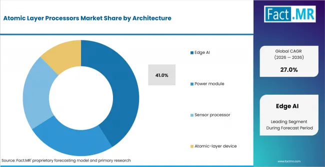
Atomic Layer Processors Market Analysis By Architecture | Source: Fact.MR
Edge AI leads because local devices need faster inference with lower leakage. Atomic-layer films help control transistor interfaces and power paths where heat budgets are tight. SIA reported in August 2026 that global semiconductor sales reached USD 403.3 billion in the second quarter of 2026, underscoring the strength of global chip demand and the semiconductor industry’s role in next-generation technology innovation.
What leads the Packaging segment?
2.5D is anticipated to account for 44.0% share in 2026.
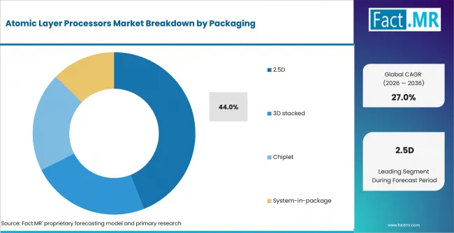
Atomic Layer Processors Market Analysis By Packaging | Source: Fact.MR
2.5D packaging is preferred because it keeps processor dies and memory close while retaining a practical validation route. HBM CoWoS packaging capacity illustrates how high-bandwidth memory and AI accelerators are raising interest in interposer-based assembly. NIST-administered CHIPS programs finalized USD 1.4 billion in advanced packaging awards in January 2025, including USD 300 million for advanced substrates and materials research and USD 1.1 billion for advanced packaging prototyping and piloting capabilities.
How does Function shape demand?
Inference is estimated to capture 44.0% share in 2026.
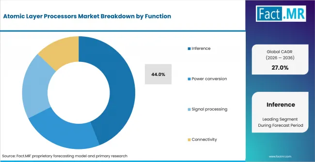
Atomic Layer Processors Market Analysis By Function | Source: Fact.MR
Inference leads because deployed AI processors must respond inside fixed thermal envelopes. On-device and edge systems do not have unlimited cooling or memory. Lam Research introduced ALTUS® Halo for molybdenum ALD in February 2025, highlighting molybdenum’s lower resistivity in nanoscale wires and its potential to improve chip speed. The development gives semiconductor process teams additional evidence for evaluating atomic-scale metallization choices in advanced devices.
What supports Automotive within End Use?
Automotive is forecast to represent 34.0% share in 2026.
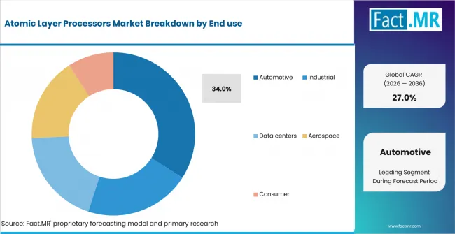
Atomic Layer Processors Market Analysis By End Use | Source: Fact.MR
Automotive holds a visible position because vehicles are adding local intelligence across powertrain and safety electronics. Atomic-layer processor designs are relevant where compact devices must manage heat, vibration and long service-life expectations. The same qualification burden slows release timing, so suppliers that document reliability evidence early have an advantage with vehicle platform teams.
What supports Discrete within Integration?
Discrete is expected to hold 52.0% share in 2026.
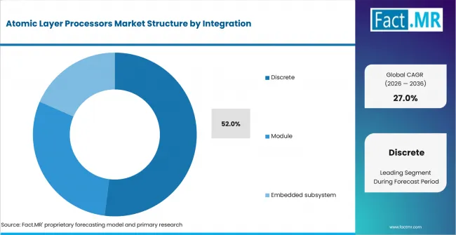
Atomic Layer Processors Market Analysis By Integration | Source: Fact.MR
Discrete integration leads because separate processor elements are easier to qualify and replace. Procurement teams can validate thermal behavior, firmware interfaces and package reliability before wider subsystem use. Demand from GPU and HPC silicon interposers reinforces the same design direction, where compute dies and memory links are evaluated as a package-level system.
What is accelerating Atomic Layer Processors Market adoption, and what is holding it back?
Adoption is rising through edge AI, 2.5D packaging and inference workloads; limits center on yield, qualification time and integration complexity.
Drivers Impact Analysis
| DRIVER | (~) % IMPACT ON CAGR | GEOGRAPHIC RELEVANCE | IMPACT TIMELINE |
|---|---|---|---|
| Edge AI processor demand in local inference | +2.4% | Global | Short term (<= 2 years) |
| 2.5D package adoption for chiplet routing | +1.8% | USA, South Korea, Japan | Medium term (2-4 years) |
| Atomic-layer deposition in advanced logic and memory | +1.5% | USA, Germany, Japan | Medium term (2-4 years) |
| Automotive electronics qualification for compact processors | +1.1% | USA, Germany, South Korea | Long term (>= 4 years) |
- Edge AI processor demand in local inference: Devices in vehicles, factories and consumer equipment need inference close to the sensor. Atomic-layer film control is expected to help reduce leakage and protect response time where cooling budgets are fixed.
- 2.5D package adoption for chiplet routing: Processor architectures rely on shorter data paths between compute and memory. NIST defined advanced packaging as many chips assembled tightly on a substrate in two or three dimensions, which matches the commercial need behind HBM silicon interposer and substrate development.
- Automotive electronics qualification: Automotive use adds long validation cycles and tight reliability demands. Suppliers that prove film stability and package-level behavior are better placed for platform approval.
Opportunity Impact Analysis
| OPPORTUNITY | (~) % IMPACT ON CAGR | GEOGRAPHIC RELEVANCE | IMPACT TIMELINE |
|---|---|---|---|
| Processor-memory co-design in 2.5D packages | +1.6% | USA, South Korea, Japan | Medium term (2-4 years) |
| ALD-based surfaces for hybrid bonding | +1.1% | Japan, USA, Germany | Long term (>= 4 years) |
| Automotive edge modules using inference processors | +0.9% | Germany, USA, South Korea | Medium term (2-4 years) |
- Processor-memory co-design in 2.5D packages: Designers bring memory closer to compute while keeping separate dies on an interposer. 3D TSV packages show how vertical interconnects support denser package routes.
- ALD-based surfaces for hybrid bonding: Atomic layer deposition can support highly controlled surface formation for hybrid bonding applications. These approaches can improve interface quality and support advanced semiconductor packaging where precise thin-film engineering is important.
- Automotive edge modules using inference processors: Vehicle platforms increasingly require local processing where thermal performance, space efficiency and reliability influence component selection. Atomic-layer processor modules can support compact packaging architectures that combine inference capability with efficient power management.
Restraints Impact Analysis
| RESTRAINT | (~) % IMPACT ON CAGR | GEOGRAPHIC RELEVANCE | IMPACT TIMELINE |
|---|---|---|---|
| Yield sensitivity in atomic-scale film control | -0.8% | Global | Short term (<= 2 years) |
| Long automotive and industrial qualification cycles | -0.6% | USA, Germany, Japan | Medium term (2-4 years) |
| Power and cooling limits in data centers and fabs | -0.5% | North America, Europe, East Asia | Long term (>= 4 years) |
- Yield sensitivity in atomic-scale film control: Small variations in thin-film thickness, interface quality or deposition uniformity can affect device reliability and slow process qualification. Manufacturers therefore need tight process control before advanced atomic-layer structures can move into high-volume production.
- Long automotive and industrial qualification cycles: Automotive and industrial applications require extensive validation for temperature tolerance, vibration resistance and service-life performance. Adoption can therefore take longer when compact processor packages combine inference, signal processing and power-conversion functions.
- Power and cooling limits in data centers and fabs: Advanced processors must deliver performance within available power and thermal envelopes. Buyers increasingly evaluate processor efficiency alongside cooling requirements, power density and infrastructure constraints when selecting architectures for data-center and semiconductor-fabrication environments.
Which countries are scaling the Atomic Layer Processors Market through 2036?
- The country comparison spans 15.0 percentage points and forms three practical growth bands across the forecast period.
- South Korea remains 4.5 percentage points above the UK as semiconductor exports and AI-chip policy deepen the local supply base.
- The UK remains 4.8 percentage points above the USA through semiconductor design depth and commercialization funding.
- The USA remains 4.0 percentage points above Germany as advanced packaging R&D and data center compute demand support processor qualification.
- Germany remains 1.7 percentage points above Japan through EU-backed semiconductor facilities and industrial electronics demand.
- Japan closes the displayed range through domestic leading-edge manufacturing support and ALD equipment capability.
Comparable CAGRs create different entry conditions due to process capacity, package qualification, public funding and semiconductor export depth. Full report coverage includes North America, Latin America, Western Europe, Eastern Europe, East Asia, South Asia & Pacific, Middle East & Africa.
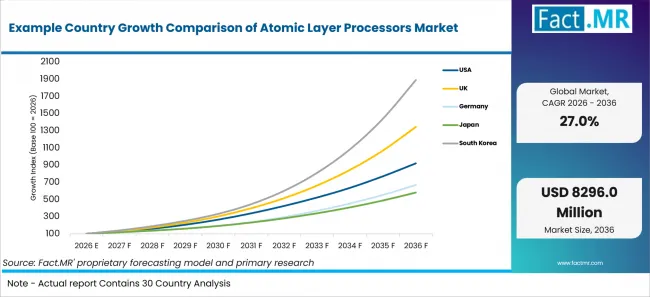
Example Country Growth Comparison Of Atomic Layer Processors Market | Source: Fact.MR
| Country | CAGR (2026-2036) |
|---|---|
| South Korea | 34.2% |
| United Kingdom | 29.7% |
| United States | 24.9% |
| Germany | 20.9% |
| Japan | 19.2% |
What supports USA adoption?
24.9% CAGR, supported by advanced packaging R&D and data center processor demand.
U.S. adoption is tied to package-level experimentation moving closer to pilot production. NIST announced in January 2025 that the Commerce Department finalized USD 1.4 billion in advanced packaging awards, including USD 1.1 billion for Natcast and USD 100 million for Applied Materials. The EIA estimated in May 2026 that servers accounted for 7% of U.S. commercial-sector electricity consumption in 2025. These signals increase the value of processors that reduce energy loss while meeting package reliability needs.
How is the United Kingdom scaling demand?
29.7% CAGR, driven by semiconductor design depth and commercialization funding.
The UK is scaling from a design and prototype base. DSIT reported in June 2026 that dedicated UK semiconductor companies generated GBP 10.6 billion in 2025 revenue and directly employed about 16,350 people. The government also announced a GBP 10 million semiconductor innovation fund in September 2025 for up to 40 businesses. That combination supports atomic-layer processor designs that need cleanroom access, verification help and a route from lab work into packaged devices.
What supports Germany’s adoption?
20.9% CAGR, supported by EU-backed semiconductor facilities and industrial electronics.
Germany’s outlook is linked to European semiconductor capacity and industrial electronics use. The European Commission approved EUR 659 million in German State aid in July 2026 for four first-of-a-kind semiconductor facilities. The measure supports facilities across the semiconductor value chain, which is relevant to processors that require precise deposition, metrology and packaging steps. Germany’s automotive and factory automation base is expected to keep qualification standards high through the forecast period.
How does Japan perform?
19.2% CAGR, led by domestic manufacturing support and ALD equipment capability.
Japan performs through precision equipment and domestic leading-edge processor programs. METI said in June 2026 that the Government of Japan executed a JPY 150 billion investment in Rapidus through the Innovation Platform Agency. Tokyo Electron released EVAROS in December 2025 for 300 mm wafers, supporting ALD and other precise deposition steps with about 25% lower CO2 emissions per wafer than the previous TELINDY PLUS system. These factors support a careful ramp path for atomic-layer processor production.
How is South Korea developing demand?
34.2% CAGR, propelled by semiconductor exports and AI-chip policy.
South Korea develops demand through export scale and targeted AI semiconductor programs. MOTIR reported in January 2026 that semiconductor exports rose 22.2% year over year to a record USD 173.4 billion in 2025. MOTIE confirmed in September 2025 that its K-On-Device AI Semiconductor Technology Development project had received a preliminary feasibility study exemption on August 22 and would begin in 2026; the ministry had earlier described the planned project in May 2025 as approximately KRW 1 trillion in scale. That policy and export mix supports processor suppliers that can serve AI modules, memory-adjacent packages and edge devices.
Who leads the Atomic Layer Processors Market?
Applied Materials is an active provider across materials engineering, advanced packaging and process-control equipment. Its June 2026 launch added CMP, deposition and eBeam systems for next-generation DRAM and advanced packaging, including SEMVision G7AP for high-resolution defect review across silicon, organic and glass substrates.
ASM International maintains significant depth in atomic layer deposition. In September 2025, ASM highlighted ALD portfolio advances including an AI/ML-enabled platform for clustered, integrated processes and applications such as selective ALD and molybdenum ALD. These capabilities support precise thin-film processing for advanced logic, foundry and memory applications.
Lam Research participates through deposition and etch equipment supporting advanced logic and memory scaling. The company introduced ALTUS Halo for molybdenum ALD in February 2025 and linked molybdenum metallization to lower nanoscale-wire resistance, fewer process steps and improved chip speed.
Tokyo Electron and Kokusai Electric add Japanese semiconductor-equipment depth. Tokyo Electron released EVAROS in December 2025 for 300 mm wafers and high-precision deposition control. Kokusai Electric reported in June 2025 that ALD-Al₂O₃ films deposited on 300 mm silicon wafers enabled direct bonding without CMP or plasma treatment. Beneq provides industrial and semiconductor ALD equipment, including production-oriented semiconductor ALD platforms.
Which companies are the key providers?
Key companies include Applied Materials, ASM International, Lam Research, Tokyo Electron, Kokusai Electric, and Beneq.
- Applied Materials
- ASM International
- Lam Research
- Tokyo Electron
- Kokusai Electric
- Beneq
Bibliography
- Semiconductor Industry Association. (2026, August 6). Global semiconductor sales increase 35.1% from Q1 2026 to Q2 2026.
- SEMI. (2026). 300mm Fab Outlook: Q2 2026 update.
- National Institute of Standards and Technology. (2025, January 16). U.S. Department of Commerce announces $1.4 billion in final awards to support the next generation of U.S. semiconductor advanced packaging.
- U.S. Energy Information Administration. (2026, May 19). Data center server energy use grows across the commercial building stock.
- Department for Science, Innovation and Technology. (2026, June 8). Semiconductor Sector Study 2026. GOV.UK.
- Department for Science, Innovation and Technology. (2025, September 24). New £10 million fund to support UK businesses to deliver next generation of semiconductors. GOV.UK.
- European Commission. (2026, July 14). Commission approves €659 million German State aid for four new semiconductor facilities.
- Ministry of Economy, Trade and Industry. (2026, June 5). Press Conference by Minister Akazawa (Excerpt).
- Ministry of Trade, Industry and Resources. (2026, January 2). Korea’s annual exports reach new highs in 2025.
- Ministry of Trade, Industry and Energy. (2025, September 30). End-users, fabless firms, and foundries join forces to build Korea’s on-device AI semiconductor ecosystem.
- Applied Materials, Inc. (2026, June 25). Applied Materials introduces new systems to accelerate DRAM and advanced packaging for AI chips.
- ASM International N.V. (2025, September 23). ASM hosts Investor Day, provides new 2030 targets, revises H2 2025 outlook.
- Lam Research Corporation. (2025, February 19). Lam Research ushers in new era of semiconductor metallization with ALTUS® Halo for molybdenum atomic layer deposition.
- Tokyo Electron Limited. (2025, December 15). Tokyo Electron releases EVAROS™, a batch thermal processing system for 300 mm wafers.
- Kokusai Electric Corporation. (2025, June 2). Joint research with YOKOHAMA National University demonstrates novel thin film and bonding process to enable energy-efficient next-generation 3D semiconductor devices.
This Report Answers
- The report explains where atomic layer processors are used across architecture, packaging, function, end use and integration choices.
- Segment analysis identifies the leading subsegments and the technical reasons semiconductor teams prioritize them.
- Country analysis examines the listed markets and the policy or manufacturing mechanisms supporting processor deployment.
- Competitive analysis reviews current providers across deposition, etch, thermal processing, packaging tools and industrial ALD equipment.
- Application analysis assesses how leakage control, package density and qualification evidence influence purchase decisions.
What does the Atomic Layer Processors Market cover?
The Atomic Layer Processors Market covers processor devices, package-level modules and embedded subsystem designs that rely on atomic-layer materials control, thin-film deposition, hybrid bonding and high-precision integration to support advanced computing functions. It includes processor architectures used for edge AI, power conversion, signal processing and connectivity, together with packaging approaches such as 2.5D, 3D stacked, chiplet and system-in-package configurations.
The assessment covers discrete, module and embedded-subsystem integration across automotive, industrial, data center, aerospace and consumer applications. Demand is assessed across architecture, packaging, function, end-use and integration segmentation, with emphasis on film uniformity, package density, thermal performance, processor-to-memory connectivity and qualification requirements.
What is included in the scope?
The scope includes processor devices, package-level processor modules and subsystem designs where ALD, hybrid bonding, interposer routing or thin-film interfaces directly affect qualification. It includes discrete and modular devices used in inference, signal processing, power conversion and connectivity functions. Adjacent HBM for automotive AI processors helps define the memory-to-processor route for vehicle AI workloads.
What is excluded from the scope?
The scope excludes general semiconductor equipment sold without a processor-specific use case. It also excludes raw wafers, base chemicals, general test services and unrelated software. Coverage of advanced IC substrates remains adjacent when the substrate is a packaging input rather than the processor product itself.
General AI-chip design software is excluded when it is sold without atomic-layer materials or package integration linkage. Coverage of 3D semiconductor packaging is treated as adjacent when the package technology supports several processor types rather than the atomic-layer processor market alone.
How Was the Analysis Built?
The analysis draws on 120+ sources, 35+ company portfolios, 25+ countries, and more than 20 industry interviews.
- Primary Research: Primary research includes discussions with manufacturers, service providers, technology developers, distributors, end users, procurement teams, and subject-matter experts. These conversations examine purchasing priorities, product adoption, operational challenges, approval requirements, competitive positioning, and the factors that influence wider market acceptance.
- Desk Research: Desk research covers government statistics, regulatory publications, company filings, trade data, technical studies, industry associations, standards, public policy, and other authoritative sources. Every source used in the analysis is documented in the bibliography.
- Market Sizing and Forecasting: Market estimates combine historical performance, demand indicators, pricing and volume trends, segment shares, company participation, country-level growth, adoption patterns, investment activity, and barriers to market expansion.
- Data Validation and Update Cycle: Findings are validated by comparing primary interviews with public data, company activity, regulatory changes, trade patterns, and industry developments. Regular updates review new product launches, capacity changes, partnerships, approvals, procurement trends, and shifts in commercial adoption.
What is the report’s scope and coverage?
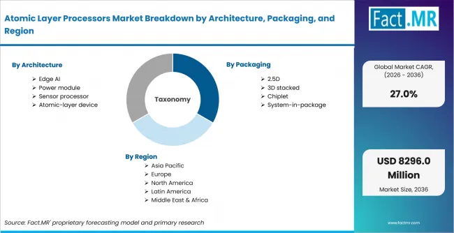
Atomic Layer Processors Market Breakdown By Architecture, Packaging, And Region | Source: Fact.MR
| Attribute | Details |
|---|---|
| Quantitative Units | USD million |
| Market Definition | Processor devices and architectures that rely on atomic-layer materials control, thin-film deposition, package-level integration and process precision to support edge AI, power conversion, signal processing and embedded compute. |
| Architecture | Edge AI; Power module; Sensor processor; Atomic-layer device |
| Packaging | 2.5D; 3D stacked; Chiplet; System-in-package |
| Function | Inference; Power conversion; Signal processing; Connectivity |
| End Use | Automotive; Industrial; Data centers; Aerospace; Consumer |
| Integration | Discrete; Module; Embedded subsystem |
| Regions Covered | North America; Latin America; Western Europe; Eastern Europe; East Asia; South Asia & Pacific; Middle East & Africa |
| Countries Covered | United States; United Kingdom; Germany; Japan; South Korea |
| Key Companies Profiled | Applied Materials; ASM International; Lam Research; Tokyo Electron; Kokusai Electric; Beneq |
| Forecast Period | 2026 to 2036 |
| Approach | Hybrid top-down and bottom-up approach using semiconductor equipment spending, advanced packaging activity, processor use cases, country adoption, segment shares and provider portfolio review. |
How is the market segmented?
-
By Architecture:
- Edge AI
- Power module
- Sensor processor
- Atomic-layer device
-
By Packaging:
- 2.5D
- 3D stacked
- Chiplet
- System-in-package
-
By Function:
- Inference
- Power conversion
- Signal processing
- Connectivity
-
By End Use:
- Automotive
- Industrial
- Data centers
- Aerospace
- Consumer
-
By Integration:
- Discrete
- Module
- Embedded subsystem
-
By Region:
- North America
- Latin America
- Western Europe
- Eastern Europe
- East Asia
- South Asia & Pacific
- Middle East & Africa