- Market Value (2025): USD 145.5 Mn
- Estimated Value (2026): USD 166.0 Mn
- Forecast Value (2036): USD 620.0 Mn
- CAGR (2026-2036):14.1%
What is the Chiplet Surface Cleaners Market forecast to be worth by 2036?
USD 166.0 million in 2026 to USD 620.0 million by 2036, at a 14.1% CAGR.
- The Chiplet Surface Cleaners Market crossed a valuation of USD 145.5 million in 2025, supported by demand from OSAT providers serving Singulation debris workflows that require cleaning singulated, often thin and mechanically compliant dies without adding stress, edge damage, residue or handling contamination.
- Demand is projected to increase from USD 166.0 million in 2026 to USD 620.0 million by 2036.
- The market is forecast to record a 14.1% CAGR from 2026 to 2036 as thin chiplets impose die-specific cleaning physics, contamination to void chain is documented and cleaning chemistry baseline remain central purchase reasons.
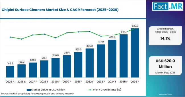
Chiplet Surface Cleaners Market Value Analysis | Source: Fact.MR
What are the defining numbers behind Chiplet Surface Cleaners Market growth?
USD 454.0 million absolute opportunity is expected by 2036.
- Demand Drivers in the Market
- Thin chiplets impose die-specific cleaning physics: Demand is shifting toward die-specific cleaning platforms because chiplets under roughly 50 micrometers flex under vacuum collets and arrive slightly curved, hindering coplanar landing; cleaning that adds stress, watermarks, or residue only worsens this, per an SMTA 2025 chiplet-bonding paper. [1]
- Contamination-to-void chain is documented: Buyers are specifying tighter cleaning because the contamination-to-void chain is now documented: inconsistent CMP/post-clean from chiplet to chiplet leaves copper-pad height and oxide uniformity variation, and recess beyond a few nanometers shifts bond force onto oxide, weakening Cu-Cu interfaces - while an inorganic protective layer integrated into the chiplet-to-wafer workflow measurably cut contamination, voids, and overlay error in the same study.
- Cleaning chemistry baseline: The cleaning chemistry baseline adapted from wafer practice - SC-1 (NH4OH/H2O2) with chelators and megasonic energy around 1.13 W/cm2 to remove 0.2 micrometer-class particles and Fe/Al/Cu/Ni/Zn metals, plus sub-5-second dilute HF to strip native oxide - is now being re-qualified for die-on-tape and reconstituted formats, anchoring procurement specs for chiplet cleaning tools. [2]
- Damage-free requirement: Tool selection is converging on megasonic frequencies of 0.8-2 MHz because smaller cavitation bubbles at higher frequency remove sub-micron particles while protecting fragile features, which is critical for exposed copper pads and fine dielectric topography on chiplet bond faces. [3]
- Key Segments Analyzed
- By Cleaning Method: Plasma die cleaning is projected to hold 32.0% share in 2026, supported by a clear process advantage: Plasma die cleaning treats the exposed chiplet surface without a liquid rinse and drying cycle, reducing the handling burden for thin or very small dies. It can remove organics and activate surfaces immediately before placement.
- By Handling Format: Die-on-carrier is projected to hold 44.8% share in 2026, supported by a clear process advantage: Die-on-carrier handling keeps singulated chiplets registered and supported during cleaning, inspection and transfer to the bonder. The carrier converts many fragile loose dies into a repeatable panel-like workpiece.
- By Contaminant Target: Singulation debris are projected to hold 38.8% share in 2026, supported by a clear process advantage: Singulation debris is specific to the chiplet flow and can include silicon fragments, tape residue and edge-generated particles. These contaminants arrive after wafer-level cleaning, so they require a dedicated die-level intervention.
- By Die Size: <5 mm die is projected to hold 41.0% share in 2026, supported by a clear process advantage: Dies below 5 millimeters create the largest count per carrier and the highest frequency of handling events. Their low mass and limited gripping area make uniform cleaning, drying and inspection more difficult.
- By End User: OSAT providers are projected to hold 30.4% share in 2026, supported by a clear process advantage: OSAT providers receive known-good dies from multiple sources and must standardize cleanliness before assembly. Their commercial role makes them responsible for converting variable incoming surfaces into a controlled bond-ready condition.
- Analyst Opinion at Fact.MR
- Shambhu Nath Jha, Sr. Consultant at Fact.MR, states, 'Buyers should evaluate the complete process sequence around cleaning singulated, often thin and mechanically compliant dies without adding stress, edge damage, residue or handling contamination. Technical review should focus on repeatability, integration, defect control and production throughput rather than a single headline specification. Suppliers that connect tool performance to measurable yield and qualification results are likely to build trust faster.'
- Strategic Implications
- Tool selection should be tied to die thickness, carrier format, contamination class and the downstream bonding interface.
- Equipment suppliers should document how their systems address the challenge of cleaning singulated, often thin and mechanically compliant dies without adding stress, edge damage, residue or handling contamination across production-representative wafers, panels, dies or packages.
- Procurement teams can compare process capability, integration burden, service coverage and qualification evidence before prioritizing nominal throughput or a single accuracy claim.
Taiwan is projected to record a 15.4% CAGR as leading foundry production, advanced packaging and a dense OSAT and substrate supply chain supports relevant capital spending; Malaysia is projected to record a 15.1% CAGR as large-scale outsourced assembly, test and package manufacturing supports relevant capital spending; South Korea is projected to record a 14.8% CAGR as high-volume memory, HBM and vertically integrated semiconductor manufacturing supports relevant capital spending; Singapore is projected to record a 14.3% CAGR as advanced-packaging R&D, specialty fabs and regional assembly and test operations supports relevant capital spending; while Vietnam is projected to record a 16.2% CAGR as expanding back-end assembly and electronics manufacturing capacity supports relevant capital spending through 2036.
How does the Chiplet Surface Cleaners Market break down by segment?
Plasma die cleaning leads Cleaning Method with a 32.0% share, while Die-on-carrier accounts for 44.8% of Handling Format in 2026.
Why does Plasma die cleaning lead Cleaning Method?
Plasma die cleaning is projected to account for 32.0% share in 2026.
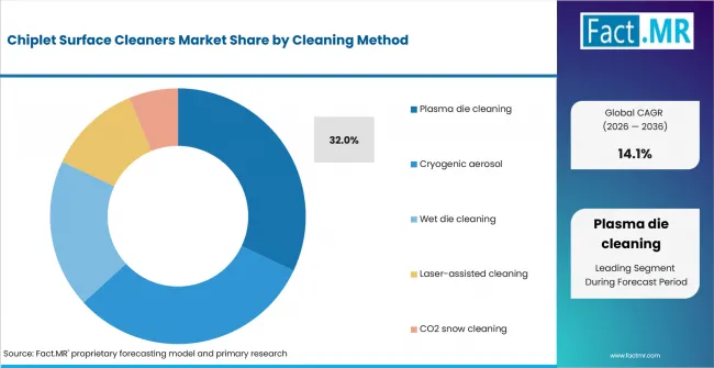
Chiplet Surface Cleaners Market Analysis By Cleaning Method | Source: Fact.MR
Plasma die cleaning treats the exposed chiplet surface without a liquid rinse and drying cycle, reducing the handling burden for thin or very small dies. It can remove organics and activate surfaces immediately before placement. Cryogenic aerosol is strong for particle removal, but it introduces a separate mechanical and handling window that must be controlled for fragile dies. Plasma (rather than wet) cleans for individual chiplets on film frames avoid drying defects on ultra-thin dies and fit directly upstream of D2W bonders. Buyers therefore tend to treat plasma die cleaning as the practical choice when qualification must balance process capability, repeatability and production economics.
Why does Die-on-carrier lead Handling Format?
Die-on-carrier is projected to account for 44.8% share in 2026.
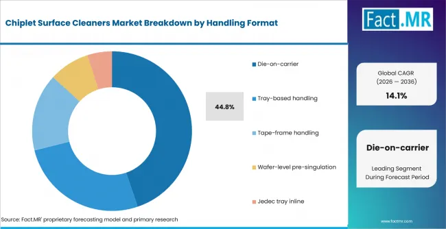
Chiplet Surface Cleaners Market Analysis By Handling Format | Source: Fact.MR
Die-on-carrier handling keeps singulated chiplets registered and supported during cleaning, inspection and transfer to the bonder. The carrier converts many fragile loose dies into a repeatable panel-like workpiece. Tray handling is flexible, but repeated pick-and-place steps add edge contact, orientation error and contamination opportunities. SC-1 (NH4OH/H2O2) with chelators and megasonic energy (~1.13 W/cm²) removes 0.2 µm-class particles and Fe/Al/Cu/Ni/Zn metals; dilute HF (<5 s, 1:100) strips native oxide; surfactants up to 0.2% - adapted from wafer practice but now applied to die-on-tape / reconstituted formats. [2] Buyers therefore tend to treat die-on-carrier as the practical choice when qualification must balance process capability, repeatability and production economics.
Why do Singulation debris lead Contaminant Target?
Singulation debris are projected to account for 38.8% share in 2026.
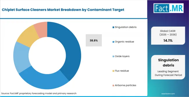
Chiplet Surface Cleaners Market Analysis By Contaminant Target | Source: Fact.MR
Singulation debris is specific to the chiplet flow and can include silicon fragments, tape residue and edge-generated particles. These contaminants arrive after wafer-level cleaning, so they require a dedicated die-level intervention. Organic residue is also important, but singulation debris more directly distinguishes chiplet cleaning from conventional wafer cleaning. Chiplets under ~50 µm flex under vacuum collets and arrive slightly curved, hindering coplanar landing; cleaning must not add stress, watermarks, or residues that worsen this (SMTA 2025 chiplet-bonding paper, §6/§10). [1] Buyers therefore tend to treat singulation debris as the practical choice when qualification must balance process capability, repeatability and production economics.
Why does <5 mm die lead Die Size?
<5 mm die is projected to account for 41.0% share in 2026.
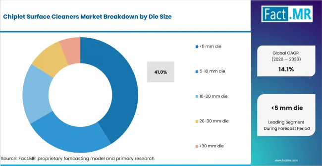
Chiplet Surface Cleaners Market Analysis By Die Size | Source: Fact.MR
Dies below 5 millimeters create the largest count per carrier and the highest frequency of handling events. Their low mass and limited gripping area make uniform cleaning, drying and inspection more difficult. Larger dies provide more area for gripping and metrology, reducing the handling intensity per cleaned surface. HBM fabrication thins memory wafers to ~50 µm, laminates wafer-level underfill over Cu-pillar bumps, dices, and TCB-stacks on a logic wafer; each stacked die is a chiplet whose surface state (solder non-wetting, voids, bump-to-pad alignment) is verified by 3D X-ray - linking surface prep quality directly to inspectable yield outcomes. [4] Buyers therefore tend to treat <5 mm die as the practical choice when qualification must balance process capability, repeatability and production economics.
Why do OSAT providers lead End User?
OSAT providers are projected to account for 30.4% share in 2026.
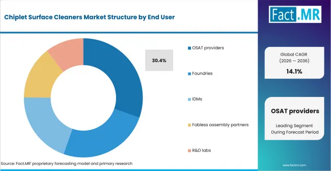
Chiplet Surface Cleaners Market Analysis By End User | Source: Fact.MR
OSAT providers receive known-good dies from multiple sources and must standardize cleanliness before assembly. Their commercial role makes them responsible for converting variable incoming surfaces into a controlled bond-ready condition. Foundries can clean within a more integrated wafer flow, whereas OSATs face greater supplier and carrier-format diversity. Inconsistent CMP/post-clean from chiplet to chiplet leaves Cu pad height and oxide uniformity variation; recess beyond a few nm shifts bond force onto oxide, weakening Cu-Cu interfaces. An inorganic protective layer integrated into the C2W workflow significantly reduced surface contamination, resulting in a lower incidence of voids and improved chiplet overlay accuracy (same paper, §7). Buyers therefore tend to treat OSAT providers as the practical choice when qualification must balance process capability, repeatability and production economics.
What is accelerating Chiplet Surface Cleaners Market adoption, and what is holding it back?
The strongest accelerator is thin chiplets impose die-specific cleaning physics, while the main restraint is that small dies and thin chiplets are harder to grip, dry and inspect uniformly, which creates a throughput-versus-damage trade-off.
Drivers Impact Analysis
| DRIVER | (~) % IMPACT ON CAGR | GEOGRAPHIC RELEVANCE | IMPACT TIMELINE |
|---|---|---|---|
| Thin chiplets impose die-specific cleaning physics | +3.9% | Global leading-edge fabs | Short term (<=2 years) |
| Contaminationtovoid chain is documented | +3.2% | Global leading-edge fabs | Medium term (2-4 years) |
| Cleaning chemistry baseline | +2.7% | Global leading-edge fabs | Medium term (2-4 years) |
| Damage-free requirement | +2.1% | Global leading-edge fabs | Medium term (2-4 years) |
Source: Fact.MR analysis. Updated Jul 22, 2026
- Thin chiplets impose die-specific cleaning physics: Chiplets under ~50 µm flex under vacuum collets and arrive slightly curved, hindering coplanar landing; cleaning must not add stress, watermarks, or residues that worsen this (SMTA 2025 chiplet-bonding paper, §6/§10). [1]
- Contaminationtovoid chain is documented: Inconsistent CMP/post-clean from chiplet to chiplet leaves Cu pad height and oxide uniformity variation; recess beyond a few nm shifts bond force onto oxide, weakening Cu-Cu interfaces. An inorganic protective layer integrated into the C2W workflow significantly reduced surface contamination, resulting in a lower incidence of voids and improved chiplet overlay accuracy (same paper, §7).
- Cleaning chemistry baseline: SC-1 (NH4OH/H2O2) with chelators and megasonic energy (~1.13 W/cm²) removes 0.2 µm-class particles and Fe/Al/Cu/Ni/Zn metals; dilute HF (<5 s, 1:100) strips native oxide; surfactants up to 0.2% - adapted from wafer practice but now applied to die-on-tape / reconstituted formats. [2]
- Damage-free requirement: Megasonic at 0.8-2 MHz with smaller cavitation bubbles removes sub-micron particles while protecting fragile features - critical for exposed Cu pads and fine dielectric topography on chiplet bond faces. [3]
Opportunity Impact Analysis
| OPPORTUNITY | (~) % IMPACT ON CAGR | GEOGRAPHIC RELEVANCE | IMPACT TIMELINE |
|---|---|---|---|
| Protective-layer workflows | +2.4% | Global leading-edge fabs | Short term (<=2 years) |
| Water-dispense assisted placement | +1.8% | Global leading-edge fabs | Medium term (2-4 years) |
| Adhesive-layer void mitigation | +1.4% | Global leading-edge fabs | Medium term (2-4 years) |
Source: Fact.MR analysis. Updated Jul 22, 2026
- Protective-layer workflows: Sacrificial inorganic layers applied before dicing and stripped in the cleaner - a documented method to decouple dicing contamination from bond-face cleanliness (SMTA 2025).
- Water-dispense assisted placement: Intel's C2W flow uses a water-dispense step with tailored surface preparation during bonding: at least 48% of dies within 200 nm, >70% within 500 nm - blurring the line between cleaner and bonder for chiplets. [1]
- Adhesive-layer void mitigation: Post-clean application of viscosity/cure-tailored adhesives conformally fills micro-trenches and residual roughness - a chemistry step sold alongside die cleaners for C2W lines (SMTA paper, §A).
Restraints Impact Analysis
| RESTRAINT | (~) % IMPACT ON CAGR | GEOGRAPHIC RELEVANCE | IMPACT TIMELINE |
|---|---|---|---|
| Primary qualification constraint | -2.1% | Global leading-edge fabs | Medium term (2-4 years) |
| Contamination and defect risk | -1.7% | Global leading-edge fabs | Short term (<=2 years) |
Source: Fact.MR analysis. Updated Jul 22, 2026
- Primary qualification constraint: Small dies and thin chiplets are harder to grip, dry and inspect uniformly, which creates a throughput-versus-damage trade-off. [1]
- Contamination and defect risk: Chiplets under ~50 µm flex under vacuum collets and arrive slightly curved, hindering coplanar landing; cleaning must not add stress, watermarks, or residues that worsen this (SMTA 2025 chiplet-bonding paper, §6/§10). [1]
- Contamination and defect risk: An inorganic protective layer integrated into the C2W workflow significantly reduced surface contamination, resulting in a lower incidence of voids and improved chiplet overlay accuracy (same paper, §7).
Which countries are scaling Chiplet Surface Cleaners Market fastest?
South Korea is projected to record a 14.8% CAGR for Chiplet Surface Cleaners Market as high-volume memory, HBM and vertically integrated semiconductor manufacturing.
- Countries differ less by the headline CAGR than by the type of semiconductor work creating demand for the Chiplet Surface Cleaners Market.
- Vietnam follows a pathway shaped by expanding back-end assembly and electronics manufacturing capacity. China takes a different path through rapid domestic capacity build-out, local-equipment substitution and tighter access to controlled foreign tools.
- Taiwan and Malaysia remain aligned through distinct combinations of device production, equipment development and advanced packaging investment.
- South Korea develops through high-volume memory, HBM and vertically integrated semiconductor manufacturing, while Singapore relies on advanced-packaging R&D, specialty fabs and regional assembly and test operations.
- Markets with similar CAGRs can follow different development paths because installed fabs, device mix, local equipment capability, export controls and qualification cycles differ.
The full report compares the six named country markets within the wider regional coverage of North America, Latin America, Europe, East Asia, South Asia & Oceania, and the Middle East & Africa.
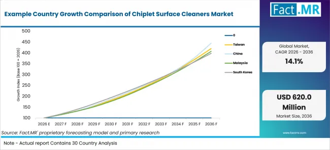
Example Country Growth Comparison Of Chiplet Surface Cleaners Market | Source: Fact.MR
| COUNTRY | CAGR, 2026 to 2036 |
|---|---|
| Vietnam | 16.2% |
| Taiwan | 15.4% |
| Malaysia | 15.1% |
| South Korea | 14.8% |
| Singapore | 14.3% |
Source: Fact.MR analysis. Updated Jul 22, 2026
What is driving Vietnam's growth through 2036?
16.2% CAGR, supported by expanding back-end assembly and electronics manufacturing capacity.
Vietnam combines expanding back-end assembly and electronics manufacturing capacity. Sacrificial inorganic layers applied before dicing and stripped in the cleaner - a documented method to decouple dicing contamination from bond-face cleanliness (SMTA 2025). The commercial link is the need to solve the problem of cleaning singulated, often thin and mechanically compliant dies without adding stress, edge damage, residue or handling contamination as capacity and process complexity increase.
What is driving Taiwan's growth through 2036?
15.4% CAGR, supported by leading foundry production, advanced packaging and a dense OSAT and substrate supply chain.
TSMC's InFO/SoIC flows drive the largest chiplet-clean demand; SoIC uses foundry-internal D2W where die-level clean specs are set in-house; ASE/SPIL run OSAT-side die cleans. This environment creates a clear qualification pathway for the Chiplet Surface Cleaners Market because buyers must solve the problem of cleaning singulated, often thin and mechanically compliant dies without adding stress, edge damage, residue or handling contamination at production scale.
What is driving Malaysia's growth through 2036?
15.1% CAGR, supported by large-scale outsourced assembly, test and package manufacturing.
Malaysia combines large-scale outsourced assembly, test and package manufacturing. Plasma (rather than wet) cleans for individual chiplets on film frames avoid drying defects on ultra-thin dies and fit directly upstream of D2W bonders. The commercial link is the need to solve the problem of cleaning singulated, often thin and mechanically compliant dies without adding stress, edge damage, residue or handling contamination as capacity and process complexity increase.
What is driving South Korea's growth through 2036?
14.8% CAGR, supported by high-volume memory, HBM and vertically integrated semiconductor manufacturing.
Samsung/SK hynix HBM4 roadmaps (TCBtohybrid bonding transition for 16-Hi stacks) pull chiplet/die-clean requirements into memory fabs. This environment creates a clear qualification pathway for the Chiplet Surface Cleaners Market because buyers must solve the problem of cleaning singulated, often thin and mechanically compliant dies without adding stress, edge damage, residue or handling contamination at production scale.
What is driving Singapore's growth through 2036?
14.3% CAGR, supported by advanced-packaging R&D, specialty fabs and regional assembly and test operations.
Singapore combines advanced-packaging R&D, specialty fabs and regional assembly and test operations. Inconsistent CMP/post-clean from chiplet to chiplet leaves Cu pad height and oxide uniformity variation; recess beyond a few nm shifts bond force onto oxide, weakening Cu-Cu interfaces. The commercial link is the need to solve the problem of cleaning singulated, often thin and mechanically compliant dies without adding stress, edge damage, residue or handling contamination as capacity and process complexity increase.
Who leads the Chiplet Surface Cleaners Market?
Nordson MARCH and PVA TePla lead the competitive landscape, followed by Plasma Etch and SCREEN Semiconductor as the next tier of challengers.
Nordson MARCH participates through plasma treatment and surface activation, with relevance determined by its ability to address the challenge of cleaning singulated, often thin and mechanically compliant dies without adding stress, edge damage, residue or handling contamination. PVA TePla participates through plasma systems and materials processing, with relevance determined by its ability to address the challenge of cleaning singulated, often thin and mechanically compliant dies without adding stress, edge damage, residue or handling contamination. Plasma Etch participates through plasma cleaning and surface treatment, with relevance determined by its ability to address the challenge of cleaning singulated, often thin and mechanically compliant dies without adding stress, edge damage, residue or handling contamination. SCREEN Semiconductor participates through single-wafer cleaning and surface preparation. Single-die and frame-mounted cleaning modules adapted from wafer platforms.
Panasonic Factory Solutions holds a more specialized role through factory automation and semiconductor assembly equipment, particularly where custom integration and service coverage affect qualification. Oxford Instruments holds a more specialized role through plasma etch, deposition and materials processing, particularly where custom integration and service coverage affect qualification.
Competition is expected to center on repeatable process performance, integration with adjacent modules, installed-base service and documented capability to address the challenge of cleaning singulated, often thin and mechanically compliant dies without adding stress, edge damage, residue or handling contamination. Buyers are likely to compare accuracy, defect prevention, throughput, recipe stability and the completeness of the delivered process cell.
Which companies are the key providers?
Key companies include Nordson MARCH; PVA TePla; Plasma Etch; SCREEN Semiconductor; Panasonic Factory Solutions; Oxford Instruments.
- Nordson MARCH
- PVA TePla
- Plasma Etch
- SCREEN Semiconductor
- Panasonic Factory Solutions
- Oxford Instruments
Bibliography
- [1] Nhanced Semi. (n.d.). Hybrid Bonding Paper Smta International 2025 Final Version V 2.
- [2] Electrochem. (n.d.). Pv 2001 26.
- [3] Modutek. (n.d.). Precision Megasonic Cleaning For Silicon Carbide Wafers.
- [4] arXiv. (n.d.). 2103.04838.
This Report Addresses
- The report provides strategic intelligence on Chiplet Surface Cleaners Market across Cleaning Method and Handling Format choices that shape purchasing decisions.
- Segment analysis covers Plasma die cleaning as the share leader within the 2026 market structure.
- Regional outlook evaluates Taiwan and China alongside Malaysia and South Korea, while Singapore and Vietnam complete the growth comparison.
- Competitive analysis profiles Nordson MARCH and PVA TePla alongside Plasma Etch and SCREEN Semiconductor, followed by additional active providers.
- Use-case assessment covers the categories and applications that shape demand in the Chiplet Surface Cleaners Market across the forecast period.
What does the Chiplet Surface Cleaners Market cover?
The market covers equipment and process systems configured to address the challenge of cleaning singulated, often thin and mechanically compliant dies without adding stress, edge damage, residue or handling contamination.
Chiplet surface cleaners are single-die and reconstituted-wafer cleaning systems that prepare singulated chiplets (not whole wafers) for hybrid bonding, thermocompression bonding, or micro-bump attach: removal of dicing residues (kerf debris, blade/dicing-tape organics, laser-grooving recast), post-grind particles, and native oxides from Cu pads - at die thicknesses down to ~50 µm or below, where wafer-style wet benches cannot be used.
Commercial value arises from the complete configured system, including process control, handling, software and integrated modules required for repeatable operation. Finished semiconductor devices, package value and unrelated parent-market equipment are excluded.
What is included in the scope?
The scope includes systems used by osat providers and the other end-user groups listed in the segmentation.
The market is segmented by Cleaning Method, including Plasma die cleaning, Cryogenic aerosol, Wet die cleaning, Laser-assisted cleaning, CO2 snow cleaning; Handling Format, including Die-on-carrier, Tray-based handling, Tape-frame handling, Wafer-level pre-singulation, Jedec tray inline; Contaminant Target, including Singulation debris, Organic residue, Oxide layers, Flux residue, Airborne particles; Die Size, including <5 mm die, 5-10 mm die, 10-20 mm die, 20-30 mm die, >30 mm die; End User, including OSAT providers, Foundries, IDMs, Fabless assembly partners, R&D labs.
Integrated handling, metrology, cleaning, activation, process-control or support modules are included when delivered as part of the configured market system.
What is excluded from the scope?
The scope excludes unrelated semiconductor equipment, standalone materials and components sold independently of the configured system.
It also excludes facility construction, cleanroom infrastructure, the value of processed wafers or packages, and adjacent process steps that are not part of the defined equipment category.
How Was the Analysis Built?
Fact.MR is of the opinion that this assessment combines structured market analysis with a review of public information and industry evidence relevant to the market.
- Market Assessment: The analysis considers demand patterns, supply conditions, segment mix, country activity, company participation, and adoption trends.
- Evidence Review: Public company disclosures, government and regulatory publications, trade information, technical literature, and industry records inform the assessment.
- Validation and Updates: Findings are cross-checked against available market indicators and reviewed when material market developments emerge.
Segmentation
What is the report's scope and coverage?
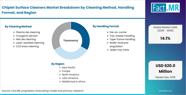
Chiplet Surface Cleaners Market Breakdown By Cleaning Method, Handling Format, And Region | Source: Fact.MR
| Attribute | Details |
|---|---|
| Quantitative Units | USD 166.0 million in 2026 to USD 620.0 million by 2036 at a 14.1% CAGR |
| Market Definition | Chiplet surface cleaners are single-die and reconstituted-wafer cleaning systems that prepare singulated chiplets (not whole wafers) for hybrid bonding, thermocompression bonding, or micro-bump attach: removal of dicing residues (kerf debris, blade/dicing-tape organics, laser-grooving recast), post-grind particles, and native oxides from Cu pads - at die thicknesses down to ~50 µm or below, where wafer-style wet benches cannot be used. |
| Cleaning Method | Plasma die cleaning; Cryogenic aerosol; Wet die cleaning; Laser-assisted cleaning; CO2 snow cleaning |
| Handling Format | Die-on-carrier; Tray-based handling; Tape-frame handling; Wafer-level pre-singulation; Jedec tray inline |
| Contaminant Target | Singulation debris; Organic residue; Oxide layers; Flux residue; Airborne particles |
| Die Size | <5 mm die; 5-10 mm die; 10-20 mm die; 20-30 mm die; >30 mm die |
| End User | OSAT providers; Foundries; IDMs; Fabless assembly partners; R&D labs |
| Regions Covered | North America; Latin America; Europe; East Asia; South Asia & Oceania; Middle East & Africa |
| Countries Covered | Taiwan; Malaysia; South Korea; Singapore; Vietnam |
| Key Companies Profiled | Nordson MARCH; PVA TePla; Plasma Etch; SCREEN Semiconductor; Panasonic Factory Solutions; Oxford Instruments |
| Forecast Period | 2026 to 2036 |
| Approach | Hybrid top-down and bottom-up approach using demand indicators across Cleaning Method; Handling Format; Contaminant Target; Die Size; End User; country-level growth; company participation and adoption trends |
Source: Fact.MR analysis. Updated Jul 22, 2026
How is the market segmented?
-
By Cleaning Method
- Plasma die cleaning
- Cryogenic aerosol
- Wet die cleaning
- Laser-assisted cleaning
- CO2 snow cleaning
-
By Handling Format
- Die-on-carrier
- Tray-based handling
- Tape-frame handling
- Wafer-level pre-singulation
- Jedec tray inline
-
By Contaminant Target
- Singulation debris
- Organic residue
- Oxide layers
- Flux residue
- Airborne particles
-
By Die Size
- <5 mm die
- 5-10 mm die
- 10-20 mm die
- 20-30 mm die
- >30 mm die
-
By End User
- OSAT providers
- Foundries
- IDMs
- Fabless assembly partners
- R&D labs
-
By Region
- North America
- Other regional markets assessed at aggregate level
- Latin America
- Other regional markets assessed at aggregate level
- Europe
- Other regional markets assessed at aggregate level
- East Asia
- Taiwan
- China
- South Korea
- South Asia & Oceania
- Malaysia
- Singapore
- Vietnam
- Middle East & Africa
- Other regional markets assessed at aggregate level
- North America
Frequently Asked Questions
Which Cleaning Method leads the Chiplet Surface Cleaners Market?
Which Handling Format leads the Chiplet Surface Cleaners Market?
Which Contaminant Target leads the Chiplet Surface Cleaners Market?
Which Die Size leads the Chiplet Surface Cleaners Market?
Which End User leads the Chiplet Surface Cleaners Market?
What CAGR is projected for Vietnam in the Chiplet Surface Cleaners Market?
What CAGR is projected for Taiwan in the Chiplet Surface Cleaners Market?
What CAGR is projected for Malaysia in the Chiplet Surface Cleaners Market?
What CAGR is projected for South Korea in the Chiplet Surface Cleaners Market?
What CAGR is projected for Singapore in the Chiplet Surface Cleaners Market?
What is the primary driver of the Chiplet Surface Cleaners Market?
What is the main restraint in the Chiplet Surface Cleaners Market?
Who worked on this report


Preview the report firsthand - request a free sample
Free SampleGet the brochure for pricing and purchase details
Download PDF