- Market Value (2025): USD 733.1 Bn
- Estimated Value (2026): USD 890 Bn
- Forecast Value (2036): USD 6188 Bn
- CAGR (2026-2036): 21.4%
What is the Chiplet Interconnect IP Market forecast to be worth by 2036?
USD 890 million in 2026 to USD 6188 million by 2036 at a 21.4% CAGR.
- The Chiplet Interconnect IP Market reached USD 733.1 million in 2025.
- Demand is projected to increase from USD 890 million in 2026 to USD 6188 million by 2036.
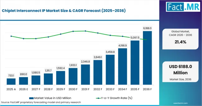
Chiplet Interconnect Ip Market Value Analysis | Source: Fact.MR
What are the defining numbers behind Chiplet Interconnect IP Market growth?
An absolute opportunity of USD 5,298 million is expected between 2026 and 2036.
- Demand Drivers in the Market
- AI and high-performance computing are increasing the use of multi-die packages because designers need more compute and memory bandwidth than a single monolithic die can provide economically. NIST identifies advanced packaging as a core enabler for recent AI systems, which directly raises the need for die-to-die interface IP that can be qualified with the package.
- UCIe is reducing interface fragmentation by defining an open die-to-die physical layer, protocol stack and compliance framework. UCIe 3.0 supports data rates up to 64 GT/s, while UCIe 2.0 added support for 3D packaging. These changes expand the range of chiplet designs that can use standardized PHY and controller IP.
- Advanced packaging capacity is expanding around AI and HPC designs. TSMC CoWoS integrates multiple logic dies with high-bandwidth memory on 2.5D structures, creating recurring demand for interconnect IP that can operate across dense package-level links.
- Design teams are seeking reusable IP to reduce the engineering work required for each new chiplet program. A licensed PHY or controller can shorten architecture development when it has already been validated for a target process, package class and UCIe revision.
- Public semiconductor programs are supporting chiplet ecosystem development. The U.S. CHIPS National Advanced Packaging Manufacturing Program explicitly includes chiplet ecosystems and co-design or EDA among its R&D areas, which supports reference flows and interoperability work that can broaden commercial IP use.
- Key Segments Analyzed
- UCIe accounts for 46.0% of Interface Standard in 2026, supported by an open specification and a growing multi-vendor interoperability ecosystem.
- PHY IP represents 52.0% of IP Type in 2026 because the physical layer carries process-specific mixed-signal complexity that many design teams prefer to license instead of develop internally.
- 2.5D interposer holds 43.0% of Packaging in 2026, reflecting its established use for integrating logic chiplets with high-bandwidth memory in AI and HPC packages.
- Data center & AI accounts for 48.0% of Application in 2026 as accelerator designs place heavy bandwidth requirements on die-to-die links and package-level memory connectivity.
- Analyst Opinion at Fact.MR
- Shambhu Nath Jha, Principal Consultant at Fact.MR, states, "Chiplet interconnect IP purchasing is moving closer to system architecture decisions because the die-to-die link must be qualified with the package and protocol stack. UCIe gives designers a common base for interoperability, but commercial selection still depends on proven PHY maturity and controller support, followed by silicon validation. Suppliers that support both 2.5D and 3D implementations while reducing verification work are likely to retain value as AI and HPC packages add more dies."
- Strategic Implications
- IP suppliers should organize UCIe offerings around the supported specification revision and package class so buyers can match a PHY or controller to a defined implementation path.
- Chiplet designers should qualify die-to-die IP alongside package planning because channel length, bump pitch and thermal constraints affect the interface before final tape-out.
- Verification IP becomes more important as UCIe adds manageability, test and debug functions across multi-chip packages, creating demand for protocol checks that extend beyond the basic data path.
- Vendors serving AI and HPC programs should document silicon validation with 2.5D packaging and high-bandwidth memory because buyers evaluate the interconnect as part of the complete compute package.
- Automotive and edge programs create a separate design path in which reliability and package cost can matter more than raw bandwidth, supporting configurable IP instead of one fixed implementation.
How does the Chiplet Interconnect IP Market break down by segment?
The market is segmented by Interface Standard, IP Type, Packaging and Application.
Why does UCIe lead Interface Standard?
UCIe leads Interface Standard in 2026.
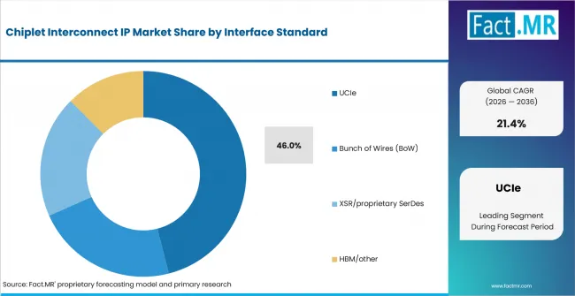
Chiplet Interconnect Ip Market Analysis By Interface Standard | Source: Fact.MR
UCIe leads because it gives semiconductor designers a common die-to-die interface across vendors and process nodes. The specification covers the physical layer and protocol stack, which reduces the amount of proprietary interface work needed when several chiplets are assembled in one package.
UCIe 2.0 added 3D packaging support and UCIe 3.0 increased the supported data rate to 64 GT/s. The continuing specification roadmap makes UCIe-based IP reusable across a wider set of multi-die programs and gives buyers a clearer interoperability target than a proprietary link.
Why does PHY IP lead IP Type?
PHY IP leads IP Type in 2026.
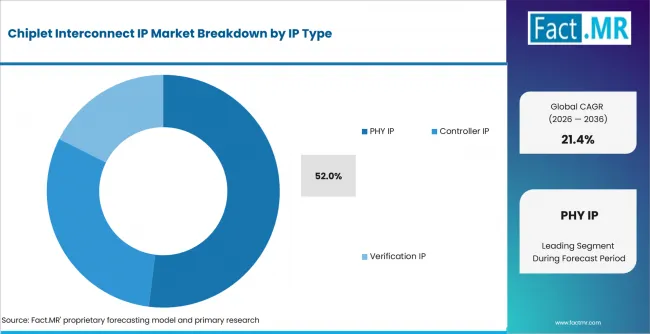
Chiplet Interconnect Ip Market Analysis By Ip Type | Source: Fact.MR
PHY IP leads because the physical layer must convert the digital interface into a high-speed electrical link that works with a specific process and package environment. Signal integrity, power efficiency and link training make this layer expensive to design and validate from scratch.
Current Synopsys and Cadence UCIe portfolios pair dedicated PHY IP with controller IP, showing how the physical layer is commercialized as a distinct licensable block. Buyers can reuse validated PHY implementations while concentrating internal engineering on the accelerator, processor or system architecture.
Why does 2.5D interposer lead Packaging?
2.5D interposer leads Packaging in 2026.
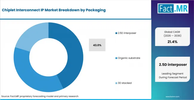
Chiplet Interconnect Ip Market Analysis By Packaging | Source: Fact.MR
2.5D interposers lead because they provide dense connections between logic chiplets and memory while keeping the dies side by side. This is useful for accelerator packages that need high bandwidth without stacking every active die vertically.
TSMC CoWoS is an established 2.5D platform that integrates multiple logic dies and high-bandwidth memory through an interposer structure. That installed packaging route gives IP suppliers a defined environment in which to qualify die-to-die PHYs and controller interfaces. 3D stacking is expanding, but it uses a different physical integration path and remains a separate design choice.
Why does Data center & AI lead Application?
Data center & AI leads Application in 2026.
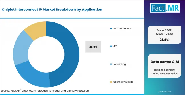
Chiplet Interconnect Ip Market Analysis By Application | Source: Fact.MR
Data center and AI systems lead because accelerator architectures need substantial compute throughput and memory bandwidth within a constrained power envelope. Multi-die packaging lets designers combine compute, memory and I/O functions without placing every function on one monolithic die.
NIST notes that recent AI advances rely on advanced packaging, while UCIe 3.0 increased die-to-die data rates for high-performance chiplet systems. These requirements make proven interface IP commercially useful because design teams can reduce link-development work while concentrating on system-level differentiation.
What is accelerating Chiplet Interconnect IP Market adoption, and what is holding it back?
Drivers Impact Analysis
| Driver | (~) % Impact on CAGR | Geographic Relevance | Impact Timeline |
|---|---|---|---|
| AI accelerator and data center multi-die package adoption | +2.1% | North America, East Asia | Near term |
| UCIe standardization lowering die-to-die integration risk | +1.8% | Global | Near term |
| HBM and high-bandwidth memory interface demand | +1.5% | Global | Mid term |
| Public CHIPS Act and heterogeneous-integration funding | +1.1% | North America, East Asia | Mid term |
Source: Fact.MR analysis. Updated Aug 19, 2026
Opportunity Impact Analysis
| Opportunity | (~) % Impact on CAGR | Geographic Relevance | Impact Timeline |
|---|---|---|---|
| UCIe-compliant PHY and controller IP licensing for AI chiplets | +1.7% | North America, East Asia | Near term |
| Verification IP for die-to-die and HBM interfaces in large packages | +1.2% | Global | Mid term |
| Interconnect IP for automotive and edge heterogeneous packages | +0.9% | North America, Europe | Long term |
Source: Fact.MR analysis. Updated Aug 19, 2026
Restraints Impact Analysis
| Restraint | (~) % Impact on CAGR | Geographic Relevance | Impact Timeline |
|---|---|---|---|
| High engineering cost and design complexity of PHY IP development | -1.0% | Global | Near term |
| Packaging-capacity and yield constraints limiting 2.5D and 3D adoption outside established foundries | -0.8% | Asia-Pacific, Europe | Mid term |
| Proprietary interface competition and fragmentation delaying standardized volume adoption | -0.6% | Global | Long term |
Source: Fact.MR analysis. Updated Aug 19, 2026
Which countries are scaling the Chiplet Interconnect IP Market through 2036?
- United States: CHIPS for America includes a dedicated advanced-packaging program with work on chiplet ecosystems and electronic design automation. This supports domestic multi-die development and creates more programs in which commercial interface IP can be evaluated and licensed.
- Taiwan: TSMC continues to expand CoWoS and other advanced packaging technologies used for AI and HPC packages. The proximity of foundry, packaging and design-service capabilities supports repeated qualification of die-to-die IP across new chiplet programs.
- Japan: METI places chiplet technology within its advanced-packaging semiconductor strategy. Public support for next-generation logic and packaging gives local design teams a clearer path from research into multi-die implementation.
- South Korea: Government-backed semiconductor standardization work now includes packaging processes, while the domestic memory industry continues to develop HBM products. These capabilities increase the need for package-level interface validation in AI-oriented designs.
- Israel: The Israel Innovation Authority identifies chip design as a major concentration within the local semiconductor workforce. A design-heavy ecosystem supports demand for licensable PHY and controller IP because fabless teams can integrate proven interface blocks into new networking and AI silicon.
- Netherlands: The 2026 National Semiconductor Vision and related Dutch technology programs place emphasis on heterogeneous integration, advanced packaging and chiplet architectures. This supports design activity that requires interoperable package-level interfaces.
Country CAGR (2026-2036)
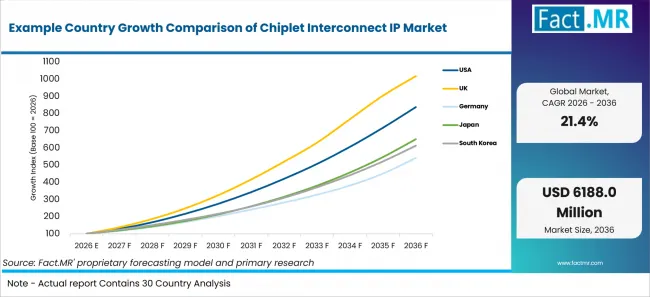
Example Country Growth Comparison Of Chiplet Interconnect Ip Market | Source: Fact.MR
| Country | CAGR (2026-2036) |
|---|---|
| United States | 21.99% |
| Taiwan | 23.74% |
| Japan | 20.74% |
| South Korea | 22.56% |
| Israel | 23.36% |
| Netherlands | 21.31% |
Source: Fact.MR analysis. Updated Aug 19, 2026
What is driving United States' growth through 2036?
The United States is forecast to expand at a 21.99% CAGR from 2026 to 2036.
Demand conditions include domestic investment in advanced packaging and chiplet co-design. The CHIPS National Advanced Packaging Manufacturing Program includes a chiplet ecosystem R&D area alongside co-design and EDA, which can increase the number of U.S. programs evaluating standardized die-to-die links. Semiconductor IP vendors benefit when design teams can qualify licensed PHY and controller blocks against common package and interoperability targets.
What is driving Taiwan's growth through 2036?
Taiwan is forecast to expand at a 23.74% CAGR from 2026 to 2036.
Taiwan combines advanced foundry processes with established 2.5D and 3D packaging. TSMC CoWoS integrates logic chiplets with HBM and continues to expand for AI and HPC designs. This environment places interface IP qualification close to process and packaging development, which supports repeated licensing as new multi-die programs move into production.
What is driving Japan's growth through 2036?
Japan is forecast to expand at a 20.74% CAGR from 2026 to 2036.
Japan is building advanced semiconductor capability around next-generation logic and packaging. METI includes the establishment of chiplet technology as a specific step in its advanced-packaging roadmap. This creates a direct use case for die-to-die interface IP as local research and manufacturing programs move from single-die designs toward heterogeneous packages.
What is driving South Korea's growth through 2036?
South Korea is forecast to expand at a 22.56% CAGR from 2026 to 2036.
South Korea combines HBM development with semiconductor packaging and system-design initiatives. The Korean government has expanded packaging standardization work, while domestic memory suppliers serve AI-oriented platforms. These activities increase the need to validate links between compute dies and memory. They must also validate package interfaces, supporting demand for reusable interconnect IP.
What is driving Israel's growth through 2036?
Israel is forecast to expand at a 23.36% CAGR from 2026 to 2036.
Israel has a semiconductor ecosystem weighted toward chip design. The Israel Innovation Authority reports that chip-design roles account for a substantial share of the local semiconductor workforce. That structure supports a licensing model in which fabless companies can use external PHY, controller and verification IP while concentrating internal engineering on processor, networking or accelerator functions.
What is driving the Netherlands' growth through 2036?
The Netherlands is forecast to expand at a 21.31% CAGR from 2026 to 2036.
Dutch semiconductor policy is increasing attention to heterogeneous integration and chiplet architectures. The National Semiconductor Vision 2035 and related advanced-packaging programs support research and industrial collaboration around new forms of chip integration. This creates demand for design IP that can connect dies across advanced package structures and support repeatable system integration.
Who leads the Chiplet Interconnect IP Market?
Synopsys, Inc. is an active provider through its current UCIe PHY, controller and verification IP portfolio. Its die-to-die products support standard and advanced packages, giving semiconductor designers a combined interface and verification path for multi-die systems.
Cadence Design Systems, Inc. competes with UCIe PHY and controller IP plus broader 3D-IC design flows. Arm Limited contributes system and interconnect IP around chiplet architectures, while Eliyan Corporation focuses on die-to-die PHY technology supporting UCIe, BoW and proprietary implementations.
The competitive set has changed through acquisition. Qualcomm Incorporated completed its acquisition of Alphawave Semi in December 2025 and also acquired Ventana Micro Systems in December 2025. These businesses should therefore be treated as part of Qualcomm instead of two independent competitors. Alphawave assets add wired connectivity and chiplet technology, while Ventana adds RISC-V compute-chiplet expertise.
Competition depends on silicon validation and package compatibility. Buyers also assess protocol support and verification coverage, with the final choice often tied to the foundry process and package architecture selected for the chiplet program.
Which companies are the key providers?
- Synopsys, Inc.
- Cadence Design Systems, Inc.
- Arm Limited
- Eliyan Corporation
- Qualcomm Incorporated
Research Sources and Bibliography
- UCIe Consortium. (2025). Specifications: Universal Chiplet Interconnect Express. UCIe Consortium.
- Open Compute Project Foundation. (2026). Bunch of Wires (BoW) PHY Specification 2.0. Open Compute Project Foundation.
- National Institute of Standards and Technology. (2026). National Advanced Packaging Manufacturing Program. U.S. Department of Commerce.
- National Institute of Standards and Technology. (2024). CHIPS National Advanced Packaging Manufacturing Program Proposer's Day. U.S. Department of Commerce.
- Defense Advanced Research Projects Agency. (2026). Common Heterogeneous Integration and IP Reuse Strategies (CHIPS). U.S. Department of Defense.
- Taiwan Semiconductor Manufacturing Company. (2026). CoWoS Advanced Packaging Technology. TSMC.
- Ministry of Economy, Trade and Industry. (2026). Outline of Semiconductor Revitalization. Government of Japan.
- Ministry of Trade, Industry and Resources. (2025). Korea Accelerates International Standardization of Semiconductor Packaging Processes. Government of the Republic of Korea.
- Israel Innovation Authority. (2025). The Semiconductor Industry in Israel. Israel Innovation Authority.
- Government of the Netherlands. (2026). National Semiconductor Vision 2035: Ambitions for the Dutch Semiconductor Industry. Ministry of Economic Affairs.
- Synopsys, Inc. (2026). UCIe PHY IP and UCIe Controller IP. Synopsys, Inc.
- Cadence Design Systems, Inc. (2026). UCIe PHY and UCIe Controller. Cadence Design Systems, Inc.
- Arm Limited. (2025). Chiplets Are Here and They Are Reshaping Everything. Arm.
- Eliyan Corporation. (2024). Eliyan Delivers 64Gbps Chiplet Interconnect PHY in 3nm Process. Eliyan Corporation.
- Qualcomm Incorporated. (2025). Qualcomm Completes Acquisition of Alphawave Semi. Qualcomm Incorporated.
- Qualcomm Incorporated. (2025). Qualcomm Acquires Ventana Micro Systems, Deepening RISC-V CPU Expertise. Qualcomm Incorporated.
This Report Answers
- The report examines demand for chiplet interconnect IP across Interface Standard and IP Type. It also covers Packaging and Application.
- Segment analysis explains the operational reasons behind the 2026 leadership of the principal subsegments.
- Country analysis compares growth across the United States and Taiwan. It also covers Japan and South Korea, with Israel and the Netherlands included through 2036.
- Competitive analysis reviews current interconnect-IP suppliers and accounts for completed acquisitions that changed the provider field.
- Application analysis assesses die-to-die interface requirements across data center and AI workloads. It also covers HPC and networking, together with automotive or edge chiplet designs.
What does the Chiplet Interconnect IP Market cover?
The Chiplet Interconnect IP Market covers licensable semiconductor intellectual property used to connect multiple dies within a package. It includes PHY, controller and verification blocks for UCIe, BoW, XSR or proprietary SerDes, and HBM or other interconnect interfaces included in the market scope.
The market covers IP deployed with 2.5D interposers, organic substrates and 3D stacked packages across data center and AI, HPC, networking, and automotive or edge applications.
What is included in the scope?
The scope includes die-to-die PHY IP and controller IP sold or licensed for chiplet integration. Verification IP is included where it validates protocol behavior, link training or interoperability for the covered interfaces.
Coverage includes interconnect IP for 2.5D, organic-substrate and 3D package routes used by semiconductor designers, IP licensees and system developers.
What is excluded from the scope?
The scope excludes chiplet manufacturing and advanced-packaging fabrication. Foundry or OSAT revenue is excluded unless tied directly to licensable interconnect IP.
Processor-core IP, memory-core IP and finished chiplet products are outside the market when they are sold without a separately identifiable die-to-die interface IP component. Standalone test engineering services and package assembly services are also excluded.
How Was the Analysis Built?
Fact.MR is of the opinion that this assessment combines primary research with a structured review of public information and industry evidence relevant to the market.
- Primary Research: Interviews focus on semiconductor IP suppliers, SoC and chiplet architects, advanced-packaging engineers, EDA specialists and licensing or procurement teams. The discussions examine interface selection, process qualification, package compatibility and commercial licensing criteria.
- Desk Research: The review covers UCIe and BoW specifications, advanced-packaging programs, national semiconductor strategies and official company documentation for current PHY, controller and verification IP. Completed acquisitions are checked against company announcements before publication.
- Market Sizing and Forecasting: Estimates combine licensable interconnect-IP revenue with semiconductor design activity. The model reviews interface mix, package adoption, licensing and royalty structures, application demand and country-level growth through 2036.
- Data Validation and Update Cycle: Evidence is reviewed against the defined market scope, segment boundaries and forecast period. The assessment is updated when source data, technology conditions, regulation or supplier activity materially changes the outlook.
Segmentation
Research Scope and Coverage
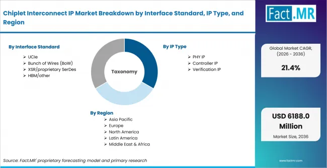
Chiplet Interconnect Ip Market Breakdown By Interface Standard, Ip Type, And Region | Source: Fact.MR
| Attribute | Details |
|---|---|
| Quantitative Units | USD 890 million in 2026 to USD 6,188 million by 2036 at a 21.4% CAGR |
| Market Definition | Licensable semiconductor IP that implements die-to-die or package-level interconnect functions for chiplet systems. Coverage includes PHY, controller and verification IP across UCIe, Bunch of Wires, XSR or proprietary SerDes, and HBM or other interconnect interfaces included in the market scope. |
| Segments Covered | Interface Standard; IP Type; Packaging; Application |
| Regions Covered | North America; Latin America; Western Europe; Eastern Europe; East Asia; South Asia & Pacific; Middle East & Africa |
| Countries Covered | United States; Taiwan; Japan; South Korea; Israel; Netherlands |
| Key Companies Profiled | Synopsys, Inc.; Cadence Design Systems, Inc.; Arm Limited; Eliyan Corporation; Qualcomm Incorporated |
| Forecast Period | 2026 to 2036 |
| Approach | Hybrid top-down and bottom-up approach using IP licensing demand, semiconductor design starts, interface mix, package adoption, country growth and company portfolio review. |
Source: Fact.MR analysis. Updated Aug 19, 2026
Market Breakdown by Segments
-
By Interface Standard
- UCIe
- Bunch of Wires (BoW)
- XSR/proprietary SerDes
- HBM/other
-
By IP Type
- PHY IP
- Controller IP
- Verification IP
-
By Packaging
- 2.5D interposer
- Organic substrate
- 3D stacked
-
By Application
- Data center & AI
- HPC
- Networking
- Automotive/edge
-
By Region
- North America
- Latin America
- Western Europe
- Eastern Europe
- East Asia
- South Asia & Pacific
- Middle East & Africa
Frequently Asked Questions
What is the Chiplet Interconnect IP Market value in 2026?
At what CAGR is the market projected to grow?
What is the projected market value by 2036?
Which Interface Standard leads the market?
Which IP Type leads the market?
Which Packaging category leads the market?
Which Application category leads the market?
Which listed country has the leading CAGR?
What is the primary driver in this market?
What is the main restraint?
Which companies are included in the market assessment?
Who worked on this report


Preview the report firsthand - request a free sample
Free SampleGet the brochure for pricing and purchase details
Download PDF