- Market Value (2025): USD 273.0 Mn
- Estimated Value (2026): USD 312.0 Mn
- Forecast Value (2036): USD 312.0 Mn
- CAGR (2026-2036): 14.3%
What is the Chiplet Bond Inspection Market forecast to be worth by 2036?
USD 312.0 million in 2026 to USD 1,185.0 million by 2036, at a 14.3% CAGR.
- The Chiplet Bond Inspection Market crossed a valuation of USD 273.0 million in 2025, supported by demand from OSAT providers serving Post-bond inline workflows that require finding buried voids, delamination, cracks and misalignment without destroying expensive multi-die packages.
- Demand is projected to increase from USD 312.0 million in 2026 to USD 1,185.0 million by 2036.
- The market is forecast to record a 14.3% CAGR from 2026 to 2036 as documented inspection workflows, post-bond acoustic checks and proven sub-micrometer X-ray capability shape equipment selection.
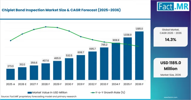
Chiplet Bond Inspection Market Value Analysis | Source: Fact.MR
What are the defining numbers behind Chiplet Bond Inspection Market growth?
USD 873.0 million absolute opportunity is expected by 2036.
- Demand Drivers in the Market
- Inspection hierarchy (documented FA workflow): Fabs are standardizing on a defined inspection sequence rather than ad hoc testing, driving demand for tools built to slot into that workflow: C-SAM runs first as a high-throughput, full-area screen, followed by 2D X-ray for gross voids and bridging, X-ray CT for 3D void distribution, IR transmission where the stack allows it, and destructive cross-section/FIB/SEM/TEM last, aimed at coordinates the non-destructive steps already found. [1]
- Post-bond acoustic check is process-of-record: Acoustic microscopy has become the process-of-record check after the roughly 350 degrees C anneal, because it gives an unambiguous pass/fail signal - voids appear as white specs against the black image of a void-free bond - making C-SAM throughput and resolution a direct purchase driver for high-volume lines. [2]
- Sub-µm X-ray is now proven on real products: Demand for sub-micron X-ray capability is accelerating now that it has been proven on real products: at the IEEE Hybrid Bonding Symposium, Excillum demonstrated nano-CT/laminography with under-100 nm voxels on an Nvidia GV100 HBM stack and an AMD Ryzen 7 5800X3D, resolving individual 1.5 micrometer hybrid copper bonds at 9 micrometer pitch. [3]
- Quantitative production-style results: Buyers are increasingly evaluating tools on throughput-versus-resolution trade-offs rather than resolution alone: Comet/Dragonfly researchers ran a 30-second overview scan at 2.6 micrometer voxels for an alignment and missing-bump screen, then a 75-minute scan at 600 nm voxels that segmented 1,275 micro-bumps and 1,680 voids by volume, aspect ratio, and sphericity - a template for production-representative qualification. [4]
- Key Segments Analyzed
- By Inspection Technique: Scanning acoustic microscopy is projected to hold 30.0% share in 2026, supported by a clear process advantage: Scanning acoustic microscopy is highly sensitive to interfacial voids and delamination because acoustic reflection changes sharply at an air gap. This supports rapid full-area screening before slower three-dimensional analysis.
- By Defect Type: Interface voids are projected to hold 49.6% share in 2026, supported by a clear process advantage: Interface voids directly reduce bonded area and can propagate under thermal cycling or block electrical contacts. A detected void can expose particle contamination, surface-preparation gaps or non-uniform bonding pressure.
- By Inspection Stage: Post-bond inline is projected to hold 47.3% share in 2026, supported by a clear process advantage: Post-bond inline inspection catches a bad interface before molding, underfill, further stacking or final test adds cost. The timing gives process teams feedback before downstream value accumulates.
- By Throughput Class: High-volume inline is projected to hold 38.7% share in 2026, supported by a clear process advantage: High-volume inline systems create value by screening enough product to influence lot disposition and process control, rather than merely producing high-resolution failure-analysis images. Automation and recipe changeover are therefore as important as image quality.
- By End User: OSAT providers are projected to hold 33.7% share in 2026, supported by a clear process advantage: OSAT providers assemble dies from multiple suppliers and bear the cost of discovering a bond defect after additional package value has been added. For OSATs, this creates an independent acceptance point before further assembly.
- Analyst Opinion at Fact.MR
- Shambu Nath Jha, Sr. Consultant at Fact.MR, states, 'Inspection strategy should match each defect to the earliest economical detection point. Acoustic methods can screen broad bonded areas, while X-ray, infrared and electron-beam techniques add detail where geometry or material stacks require it. Buyers should compare defect sensitivity, field of view, cycle time, automation and integration using production-representative packages.'
- Strategic Implications
- Inspection plans should be built around defect escape cost and the stage at which a bad interface can still be reworked or scrapped economically.
- Equipment suppliers should document how their systems address the challenge of finding buried voids, delamination, cracks and misalignment without destroying expensive multi-die packages across production-representative wafers, panels, dies or packages.
- Procurement teams can compare process capability, integration burden, service coverage and qualification evidence before prioritizing nominal throughput or a single accuracy claim.
Taiwan is projected to record a 15.6% CAGR as leading foundry production, advanced packaging and a dense OSAT and substrate supply chain supports relevant capital spending; South Korea is projected to record a 15.1% CAGR as high-volume memory, HBM and vertically integrated semiconductor manufacturing supports relevant capital spending; Malaysia is projected to record a 15.2% CAGR as large-scale outsourced assembly, test and package manufacturing supports relevant capital spending; Singapore is projected to record a 14.5% CAGR as advanced-packaging R&D, specialty fabs and regional assembly and test operations support relevant capital spending; while Japan is projected to record a 14.9% CAGR as semiconductor equipment, materials, inspection and memory-process expertise supports relevant capital spending through 2036.
How does the Chiplet Bond Inspection Market break down by segment?
Scanning acoustic microscopy leads Inspection Technique with a 30.0% share, while Interface voids account for 49.6% of Defect Type in 2026.
Why does Scanning acoustic microscopy lead Inspection Technique?
Scanning acoustic microscopy is projected to account for 30.0% share in 2026.
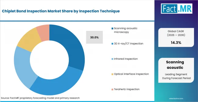
Chiplet Bond Inspection Market Analysis By Inspection Technique | Source: Fact.MR
Scanning acoustic microscopy is highly sensitive to interfacial voids and delamination because acoustic reflection changes sharply at an air gap. It can screen bonded areas without the radiation dose and reconstruction time of full 3D X-ray. X-ray and CT provide richer three-dimensional geometry, but they are generally slower and may be less sensitive to very thin planar separations. After ~350 °C anneal, acoustic microscopy can check the quality of the bond. Voids will appear as white specs, whereas a void-free bond results in a black acoustic microscopy image (Semiconductor Engineering). [2] Its speed and sensitivity make it suitable for broad post-bond screening, with X-ray reserved for defects requiring volumetric detail.
Why do Interface voids lead Defect Type?
Interface voids are projected to account for 49.6% share in 2026.
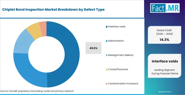
Chiplet Bond Inspection Market Analysis By Defect Type | Source: Fact.MR
Interface voids directly reduce bonded area and can propagate under thermal cycling or block electrical contacts. Their presence also indicates upstream particle, surface-preparation or pressure non-uniformity. Delamination is a related failure mode, but void detection often provides the earlier process signal before a larger separation develops. Interface-void data also helps process teams trace defects to contamination, surface preparation or bonding-pressure control.
Why does Post-bond inline lead Inspection Stage?
Post-bond inline is projected to account for 47.3% share in 2026.
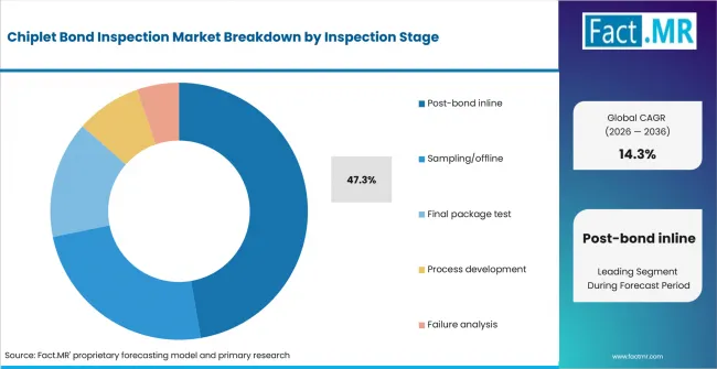
Chiplet Bond Inspection Market Analysis By Inspection Stage | Source: Fact.MR
Post-bond inline inspection catches a bad interface before molding, underfill, further stacking or final test adds cost. It also returns defect data quickly enough to adjust the current bonding process. Offline sampling supports deeper analysis but can allow a systematic excursion to continue across many packages. X-ray inspection can assess die shift and void distribution within a single study, potentially reducing separate tool passes. This stage balances early defect containment with feedback fast enough to support process correction.
Why does High-volume inline lead Throughput Class?
High-volume inline is projected to account for 38.7% share in 2026.
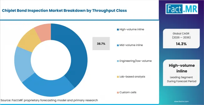
Chiplet Bond Inspection Market Analysis By Throughput Class | Source: Fact.MR
High-volume inline systems create value by screening enough product to influence lot disposition and process control, rather than merely producing high-resolution failure-analysis images. Automation and recipe changeover are therefore as important as image quality. Mid-volume tools can use longer acquisition times, but they provide less protection against low-frequency defects in mass production. The standard sequence: C-SAM first (high-throughput, full-area screen; µm-class lateral resolution; detects voids/delamination/unbonded area), then 2D X-ray (gross voids, bridging, foreign material), then X-ray CT (3D void distribution, sub-µm to µm), then IR transmission where the stack is IR-transparent; destructive cross-section/FIB/SEM/TEM last, aimed at coordinates found non-destructively. [1] Its value depends on stable recipes, automated handling and sufficient sensitivity at production cycle times.
Why do OSAT providers lead End User?
OSAT providers are projected to account for 33.7% share in 2026.
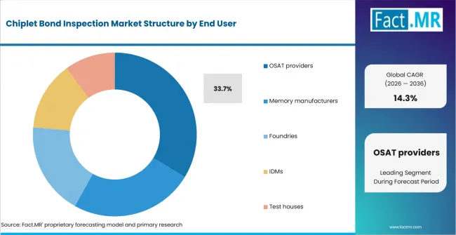
Chiplet Bond Inspection Market Analysis By End User | Source: Fact.MR
OSAT providers assemble dies from multiple suppliers and bear the cost of discovering a bond defect after additional package value has been added. Inline inspection gives them an independent acceptance layer between bonding and downstream assembly. Memory manufacturers have vertically integrated process data, while OSATs need inspection that works across a broader set of package designs. At the IEEE Hybrid Bonding Symposium, Excillum demonstrated nano-CT/laminography with <100 nm voxels (150 nm JIMA resolution) on (i) an Nvidia GV100 HBM stack - 8 DRAM layers, 20 µm micro-bumps, resolving voids and cracks - and (ii) an AMD Ryzen 7 5800X3D, resolving individual 1.5 µm hybrid Cu bonds at 9 µm pitch. [3] OSAT demand therefore favors inspection platforms that can qualify multiple package designs without sacrificing traceability or throughput.
What is accelerating Chiplet Bond Inspection Market adoption, and what is holding it back?
The strongest accelerator is inspection hierarchy (documented FA workflow), while the main restraint is that resolution, field of view and throughput pull in opposite directions, especially for dense stacks and large packages.
Drivers Impact Analysis
| DRIVER | (~) % IMPACT ON CAGR | GEOGRAPHIC RELEVANCE | IMPACT TIMELINE |
|---|---|---|---|
| Inspection hierarchy (documented FA workflow) | +4.0% | Global leading-edge fabs | Medium term (2-4 years) |
| Post-bond acoustic check is process-of-record | +3.3% | Global leading-edge fabs | Medium term (2-4 years) |
| Sub-µm X-ray is now proven on real products | +2.7% | Global leading-edge fabs | Medium term (2-4 years) |
| Quantitative production-style results | +2.1% | Global leading-edge fabs | Medium term (2-4 years) |
Source: Fact.MR analysis. Updated Jul 22, 2026
- Inspection hierarchy (documented FA workflow): The standard sequence: C-SAM first (high-throughput, full-area screen; µm-class lateral resolution; detects voids/delamination/unbonded area), then 2D X-ray (gross voids, bridging, foreign material), then X-ray CT (3D void distribution, sub-µm to µm), then IR transmission where the stack is IR-transparent; destructive cross-section/FIB/SEM/TEM last, aimed at coordinates found non-destructively. [1]
- Post-bond acoustic check is process-of-record: After ~350 °C anneal, acoustic microscopy can check the quality of the bond. Acoustic contrast after anneal provides a rapid indication of bonded versus unbonded areas. [2]
- Sub-µm X-ray is now proven on real products: At the IEEE Hybrid Bonding Symposium, Excillum demonstrated nano-CT and laminography with voxel sizes below 100 nm on HBM and hybrid-bonded processor samples. [3]
- Quantitative production-style results: Comet/Dragonfly researchers ran a 30 s overview scan at 2.6 µm voxels (alignment/missing-bump screen) then 75 min at 600 nm voxels, segmenting 1,275 micro-bumps and 1,680 voids by volume, aspect ratio, sphericity - showing the throughput/resolution trade that defines tool positioning. [4]
Opportunity Impact Analysis
| OPPORTUNITY | (~) % IMPACT ON CAGR | GEOGRAPHIC RELEVANCE | IMPACT TIMELINE |
|---|---|---|---|
| 3D X-ray moving from FA lab toward production | +2.4% | Global leading-edge fabs | Short term (<=2 years) |
| ML-assisted 3D X-ray reconstruction | +1.9% | Global leading-edge fabs | Medium term (2-4 years) |
| E-beam voltage contrast creeping into packaging | +1.4% | Global leading-edge fabs | Medium term (2-4 years) |
Source: Fact.MR analysis. Updated Jul 22, 2026
- 3D X-ray moving from FA lab toward production: Limited-angle CT (X-plane-type) designs target targeted-layer inspection at production throughput for HBM micro-bump voids and die shift (Nordson application story). [6]
- ML-assisted 3D X-ray reconstruction: Reconstruction software can shorten acquisition-to-decision time while preserving the volumetric information required to locate buried defects. [5]
- E-beam voltage contrast: Electron-beam inspection can complement package inspection where electrical opens require localized review, although its role is narrower than acoustic or X-ray screening. [7]
Restraints Impact Analysis
| RESTRAINT | (~) % IMPACT ON CAGR | GEOGRAPHIC RELEVANCE | IMPACT TIMELINE |
|---|---|---|---|
| Primary qualification constraint | -2.1% | Global leading-edge fabs | Medium term (2-4 years) |
| Workflow escalation cost | -1.7% | Global leading-edge fabs | Medium term (2-4 years) |
| False-negative risk | -1.3% | Global leading-edge fabs | Medium term (2-4 years) |
Source: Fact.MR analysis. Updated Jul 22, 2026
- Primary qualification constraint: Resolution, field of view and throughput pull in opposite directions, especially for dense stacks and large packages. [1]
- Workflow escalation cost: When broad-area screening cannot localize a defect, analysis progresses to slower X-ray CT or destructive cross-section methods, increasing cycle time and cost. [1]
- False-negative risk: Thin interfaces and complex material stacks can reduce contrast, so acoustic results may need confirmation through X-ray, infrared or destructive analysis. [1][2]
Which countries are scaling Chiplet Bond Inspection Market fastest?
In Japan, Chiplet Bond Inspection Market is projected to advance at 14.9% CAGR, supported by semiconductor equipment, materials, inspection and memory-process expertise.
- Countries differ less by the headline CAGR than by the type of semiconductor work creating demand for the Chiplet Bond Inspection Market.
- China follows a pathway shaped by rapid domestic capacity build-out, local-equipment substitution and tighter access to controlled foreign tools. Taiwan takes a different path through leading foundry production, advanced packaging and a dense OSAT and substrate supply chain.
- Malaysia and South Korea remain aligned through distinct combinations of device production, equipment development and advanced packaging investment.
- Japan develops through semiconductor equipment, materials, inspection and memory-process expertise, while Singapore relies on advanced-packaging R&D, specialty fabs and regional assembly and test operations.
- Markets with similar CAGRs can follow different development paths because installed fabs, device mix, local equipment capability, export controls and qualification cycles differ.
The full report compares the five named country markets within the wider regional coverage of North America, Latin America, Europe, East Asia, South Asia & Oceania, and the Middle East & Africa.
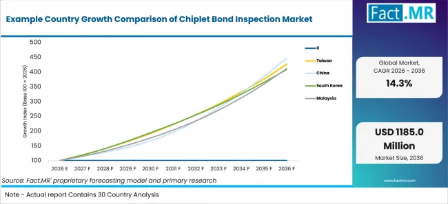
Example Country Growth Comparison Of Chiplet Bond Inspection Market | Source: Fact.MR
| COUNTRY | CAGR, 2026 to 2036 |
|---|---|
| Taiwan | 15.6% |
| Malaysia | 15.2% |
| South Korea | 15.1% |
| Japan | 14.9% |
| Singapore | 14.5% |
Source: Fact.MR analysis. Updated Jul 22, 2026
What is driving Taiwan's growth through 2036?
15.6% CAGR, supported by leading foundry production, advanced packaging and a dense OSAT and substrate supply chain.
Taiwanese foundries and OSATs require inspection tools that can qualify fine-pitch bonding processes while protecting high-value multi-die assemblies.
What is driving Malaysia's growth through 2036?
15.2% CAGR, supported by large-scale outsourced assembly, test and package manufacturing.
What is driving South Korea's growth through 2036?
15.1% CAGR, supported by high-volume memory, HBM and vertically integrated semiconductor manufacturing.
South Korea combines high-volume memory, HBM and vertically integrated semiconductor manufacturing with a 15.5% share of 2026 demand across the five profiled countries. Combining die-shift and void analysis within one X-ray workflow can reduce separate inspection steps. The commercial link is the need to solve the problem of finding buried voids, delamination, cracks and misalignment without destroying expensive multi-die packages as capacity and process complexity increase.
What is driving Japan's growth through 2036?
14.9% CAGR, supported by semiconductor equipment, materials, inspection and memory-process expertise.
Japan's inspection, microscopy and semiconductor-equipment base supports failure analysis and process-control demand for advanced packaging.
What is driving Singapore's growth through 2036?
14.5% CAGR, supported by advanced-packaging R&D, specialty fabs and regional assembly and test operations.
Singapore combines advanced-packaging R&D, specialty fabs and regional assembly and test operations with an 11.0% share of 2026 demand across the five profiled countries. After ~350 °C anneal, acoustic microscopy can check the quality of the bond. [2] The commercial link is the need to solve the problem of finding buried voids, delamination, cracks and misalignment without destroying expensive multi-die packages as capacity and process complexity increase.
Who leads the Chiplet Bond Inspection Market?
Nordson Test & Inspection and Hitachi High-Tech lead the competitive landscape, followed by Camtek and Zeiss as the next tier of challengers.
Nordson Test & Inspection offers X-ray and acoustic inspection systems for optically hidden package features, including micro-bumps and TSVs. [6]
Hitachi High-Tech provides semiconductor measurement and inspection systems, including CD-SEM and defect-inspection platforms. [8]
Camtek supplies combined 2D and 3D inspection and metrology platforms for advanced-packaging production. [9]
Zeiss provides non-destructive 3D X-ray microscopy for semiconductor-package development and failure analysis. [10]
Bruker supplies non-destructive X-ray metrology for semiconductor process monitoring, packaging structures and defect identification. [11]
Onto Innovation provides inspection, overlay and 3D metrology systems for advanced IC substrates and panel-level packaging. [12]
Competition is expected to center on repeatable process performance, integration with adjacent modules, installed-base service and documented capability to address the challenge of finding buried voids, delamination, cracks and misalignment without destroying expensive multi-die packages. Buyers are likely to compare accuracy, defect prevention, throughput, recipe stability and the completeness of the delivered process cell.
Which companies are the key providers?
Key companies include Nordson Test & Inspection; Hitachi High-Tech; Camtek; Zeiss; Bruker; Onto Innovation.
- Nordson Test & Inspection
- Hitachi High-Tech
- Camtek
- Zeiss
- Bruker
- Onto Innovation
Bibliography
- [1] NineScrolls. (2026). Hybrid Bonding Failure Analysis. https://ninescrolls.com/insights/hybrid-bonding-failure-analysis
- [2] Semiconductor Engineering. (2025). Metrology Under Pressure: Detecting Defects in Fine-Pitch Hybrid Bonding. https://semiengineering.com/metrology-under-pressure-detecting-defects-in-fine-pitch-hybrid-bonding/
- [3] IEEE.tv. (2025). Metrology for Hybrid Bonds, Microbumps and TSVs in Advanced Packaging. https://ieeetv.ieee.org/hbs/metrology-for-hybrid-bonds-microbumps-and-tsvs-in-advanced-packaging-are-x-ray-methods-up-to-the-task
- [4] ASM International. (2025). High-resolution 3D X-ray inspection for advanced packaging. https://www.asminternational.org/high-resolution-3d-x-ray-inspection-for-advanced-packaging-insights-from-hbm-micro-bump-analysis/
- [5] Zeiss. (2021). 3D X-ray Microscopy for High Resolution Measurements in Semiconductor Package Development. https://www.zeiss.com/microscopy/en/resources/insights-hub/electronics-semiconductor/3d-x-ray-microscopy-for-high-resolution-measurements.html
- [6] Nordson Test & Inspection. (2024). X-Plane Pro for non-destructive 3D inspection. https://www.nordson.com/de-de/about-us/nordson-blog/test-and-inspection-blogs/mxi-x-planvs2
- [7] KLA. (2020). KLA Introduces Breakthrough Electron-Beam Defect Inspection System. https://ir.kla.com/news-events/press-releases/detail/14/kla-introduces-breakthrough-electron-beam-defect-inspection
- [8] Hitachi High-Tech. CD-SEM & Defect Inspection. https://www.hitachi-hightech.com/global/en/products/semiconductor-manufacturing/cd-sem/
- [9] Camtek. Advanced Packaging Inspection and Metrology. https://www.camtek.com/markets/advanced-packaging/
- [10] Zeiss. 3D X-ray Microscopy for Semiconductor Packaging. https://www.zeiss.com/microscopy/en/resources/insights-hub/electronics-semiconductor/3d-x-ray-microscopy-for-high-resolution-measurements.html
- [11] Bruker. X-Ray Metrology Systems. https://www.bruker.com/de/products-and-solutions/semiconductor-solutions/x-ray-metrology-for-silicon-semi.html
- [12] Onto Innovation. Firefly G3 System. https://ontoinnovation.com/products/firefly-g3/
This Report Addresses
- The report provides strategic intelligence on Chiplet Bond Inspection Market across Inspection Technique and Defect Type choices that shape purchasing decisions.
- Segment analysis covers Scanning acoustic microscopy as the share leader within the 2026 market structure.
- Regional outlook evaluates Taiwan alongside South Korea and Malaysia, while Singapore and Japan complete the growth comparison.
- Competitive analysis profiles Nordson Test & Inspection and Hitachi High-Tech alongside Camtek and Zeiss, followed by additional active providers.
- Use-case assessment covers the categories and applications that shape demand in the Chiplet Bond Inspection Market across the forecast period.
What does the Chiplet Bond Inspection Market cover?
The market covers equipment and process systems configured to address the challenge of finding buried voids, delamination, cracks and misalignment without destroying expensive multi-die packages.
Chiplet bond inspection covers non-destructive and destructive tools that verify the integrity of chiplet-to-wafer and chiplet-to-substrate joints: scanning acoustic microscopy (C-SAM/SAT), 2D/3D X-ray (CT and laminography), IR transmission microscopy, and electrical/voltage-contrast methods - targeting voids, delamination, unbonded area, misalignment, and interfacial contamination at micro-bump and hybrid-bond interfaces.
Commercial value arises from the complete configured system, including process control, handling, software and integrated modules required for repeatable operation. Finished semiconductor devices, package value and unrelated parent-market equipment are excluded.
What is included in the scope?
The scope includes systems used by osat providers and the other end-user groups listed in the segmentation.
The market is segmented by Inspection Technique, including Scanning acoustic microscopy, 3D X-ray/CT inspection, Infrared inspection, Optical interface inspection, Terahertz inspection; Defect Type, including Interface voids, Delamination, Misalignment defects, Cracks/fractures, Contamination inclusions; Inspection Stage, including Post-bond inline, Sampling/offline, Final package test, Process development, Failure analysis; Throughput Class, including High-volume inline, Mid-volume inline, Engineering/low-volume, Lab-based analysis, Custom cells; End User, including OSAT providers, Memory manufacturers, Foundries, IDMs, Test houses.
Integrated handling, metrology, cleaning, activation, process-control or support modules are included when delivered as part of the configured market system.
What is excluded from the scope?
The scope excludes unrelated semiconductor equipment, standalone materials and components sold independently of the configured system.
It also excludes facility construction, cleanroom infrastructure, the value of processed wafers or packages, and adjacent process steps that are not part of the defined equipment category.
How Was the Analysis Built?
Fact.MR is of the opinion that this assessment combines structured market analysis with a review of public information and industry evidence relevant to the market.
- Market Assessment: The analysis considers demand patterns, supply conditions, segment mix, country activity, company participation, and adoption trends.
- Evidence Review: Public company disclosures, government and regulatory publications, trade information, technical literature, and industry records inform the assessment.
- Validation and Updates: Findings are cross-checked against available market indicators and reviewed when material market developments emerge.
Segmentation
What is the report's scope and coverage?
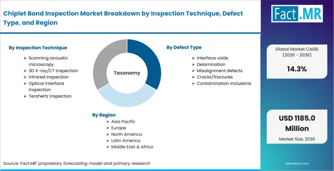
Chiplet Bond Inspection Market Breakdown By Inspection Technique, Defect Type, And Region | Source: Fact.MR
| Attribute | Details |
|---|---|
| Quantitative Units | USD 312.0 million in 2026 to USD 1,185.0 million by 2036 at a 14.3% CAGR |
| Market Definition | Chiplet bond inspection covers non-destructive and destructive tools that verify the integrity of chiplet-to-wafer and chiplet-to-substrate joints: scanning acoustic microscopy (C-SAM/SAT), 2D/3D X-ray (CT and laminography), IR transmission microscopy, and electrical/voltage-contrast methods - targeting voids, delamination, unbonded area, misalignment, and interfacial contamination at micro-bump and hybrid-bond interfaces. |
| Inspection Technique | Scanning acoustic microscopy; 3D X-ray/CT inspection; Infrared inspection; Optical interface inspection; Terahertz inspection |
| Defect Type | Interface voids; Delamination; Misalignment defects; Cracks/fractures; Contamination inclusions |
| Inspection Stage | Post-bond inline; Sampling/offline; Final package test; Process development; Failure analysis |
| Throughput Class | High-volume inline; Mid-volume inline; Engineering/low-volume; Lab-based analysis; Custom cells |
| End User | OSAT providers; Memory manufacturers; Foundries; IDMs; Test houses |
| Regions Covered | North America; Latin America; Europe; East Asia; South Asia & Oceania; Middle East & Africa |
| Countries Covered | Taiwan; South Korea; Malaysia; Singapore; Japan |
| Key Companies Profiled | Nordson Test & Inspection; Hitachi High-Tech; Camtek; Zeiss; Bruker; Onto Innovation |
| Forecast Period | 2026 to 2036 |
| Approach | Hybrid top-down and bottom-up approach using demand indicators across Inspection Technique; Defect Type; Inspection Stage; Throughput Class; End User; country-level growth; company participation and adoption trends |
Source: Fact.MR analysis. Updated Jul 22, 2026
How is the market segmented?
-
By Inspection Technique
- Scanning acoustic microscopy
- 3D X-ray/CT inspection
- Infrared inspection
- Optical interface inspection
- Terahertz inspection
-
By Defect Type
- Interface voids
- Delamination
- Misalignment defects
- Cracks/fractures
- Contamination inclusions
-
By Inspection Stage
- Post-bond inline
- Sampling/offline
- Final package test
- Process development
- Failure analysis
-
By Throughput Class
- High-volume inline
- Mid-volume inline
- Engineering/low-volume
- Lab-based analysis
- Custom cells
-
By End User
- OSAT providers
- Memory manufacturers
- Foundries
- IDMs
- Test houses
-
By Region
- North America
- Other regional markets assessed at aggregate level
- Latin America
- Other regional markets assessed at aggregate level
- Europe
- Other regional markets assessed at aggregate level
- East Asia
- Taiwan
- South Korea
- Japan
- South Asia & Oceania
- Malaysia
- Singapore
- Middle East & Africa
- Other regional markets assessed at aggregate level
- North America
Frequently Asked Questions
Which Inspection Technique leads the Chiplet Bond Inspection Market?
Which Defect Type leads the Chiplet Bond Inspection Market?
Which Inspection Stage leads the Chiplet Bond Inspection Market?
Which Throughput Class leads the Chiplet Bond Inspection Market?
Which End User leads the Chiplet Bond Inspection Market?
What CAGR is projected for China in the Chiplet Bond Inspection Market?
What CAGR is projected for Taiwan in the Chiplet Bond Inspection Market?
What CAGR is projected for Malaysia in the Chiplet Bond Inspection Market?
What CAGR is projected for South Korea in the Chiplet Bond Inspection Market?
What CAGR is projected for Japan in the Chiplet Bond Inspection Market?
What CAGR is projected for Singapore in the Chiplet Bond Inspection Market?
What is the primary driver of the Chiplet Bond Inspection Market?
What is the main restraint in the Chiplet Bond Inspection Market?
Who worked on this report


Preview the report firsthand - request a free sample
Free SampleGet the brochure for pricing and purchase details
Download PDF