- Market Value (2025): USD 205.2 Mn
- Estimated Value (2026): USD 238.0 Mn
- Forecast Value (2036): USD 1050.0 Mn
- CAGR (2026-2036): 16.0%
What is the Embedded Bridge Placement Market forecast to be worth by 2036?
USD 238.0 million in 2026 to USD 1,050.0 million by 2036, at a 16.0% CAGR.
- The Embedded Bridge Placement Market crossed a valuation of USD 205.2 million in 2025, supported by demand from OSAT providers serving Silicon bridges workflows that require placing small silicon or glass bridges into substrate cavities with micron-class registration and controlled planarity.
- Demand is projected to increase from USD 238.0 million in 2026 to USD 1,050.0 million by 2036.
- The market is forecast to record a 16.0% CAGR from 2026 to 2036 as process position and precision class, placement accuracy cascade and yield economics of placement remain central purchase reasons.
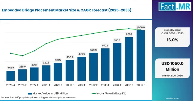
Embedded Bridge Placement Market Value Analysis | Source: Fact.MR
What are the defining numbers behind Embedded Bridge Placement Market growth?
USD 812.0 million absolute opportunity is expected by 2036.
- Demand Drivers in the Market
- Process position and precision class: Demand for dedicated bridge-placement tools stems from where this step sits in the flow: precise cavities are cut into the laminate material, small silicon bridges are then placed into them and held with a specialized adhesive - a step that happens in substrate fabs at panel scale, not in wafer fabs, and needs equipment purpose-built for that environment. [1]
- Placement accuracy cascade: Placement tolerance requirements are set by what happens downstream, not by the placement step itself: bridge placement error propagates into die attach, where fine-pitch microbumps must align to bridge pads while C4 bumps simultaneously align to substrate pads, pushing the finest bridge pad pitches toward thermocompression bonding. [3]
- Yield economics of placement: EMIB's cost and yield advantage over silicon interposers only holds if bridge embedding stays high-yield, since only the small bridge area needs to be defect-free - which is exactly why bridge placement accuracy and substrate-integration complexity are named as EMIB's defining challenges, and why buyers scrutinize placement equipment precision closely. [1]
- Bond-process control: Finetech documents sub-micrometer placement capability, while K&S describes precise heat, pressure and tilt control for fine-pitch thermo-compression bonding. These adjacent benchmarks shape bridge-placement qualification. [2][3]
- Key Segments Analyzed
- By Placement Technology: Flip-chip bonders are projected to hold 32.0% share in 2026, supported by a clear process advantage: Flip-chip bonders combine vision alignment, controlled force and thermal handling for placing a thin silicon bridge onto fine-pitch substrate features. Its vision, force and thermal-control functions provide a practical base for precision bridge handling.
- By Placement Accuracy: <1 um is projected to hold 42.1% share in 2026, supported by a clear process advantage: Sub-micrometer placement protects overlap between bridge terminals and the surrounding build-up wiring after substrate distortion and lamination are included. It also preserves routing density at the localized high-bandwidth interface.
- By Bridge Type: Silicon bridges are projected to hold 46.5% share in 2026, supported by a clear process advantage: Silicon bridges provide fine lithographic routing, mature microbump or hybrid interfaces and a thermal expansion behavior familiar to semiconductor assembly. They are the established route for localized high-density interconnect.
- By Substrate Format: Organic panel is projected to hold 44.2% share in 2026, supported by a clear process advantage: Organic panels combine the cost structure of package substrates with a local silicon bridge for high-density routing. Panel handling also supports multiple placements per workpiece and high assembly throughput.
- By End User: OSAT providers are projected to hold 32.1% share in 2026, supported by a clear process advantage: OSAT providers integrate bridge placement with die attach, molding and package assembly and can optimize the sequence around customer package designs. This operating mix favors flexible recipes, traceability and rapid product changeover.
- Analyst Opinion at Fact.MR
- Shambu Nath Jha, Sr. Consultant at Fact.MR, states, 'Bridge-placement equipment should be evaluated on post-embed registration and planarity, not only the coordinate reported when the tool releases the part. Buyers should test vision alignment, handling, adhesive control, substrate distortion, cycle time and recipe repeatability on production-representative panels. The strongest platforms will connect placement data with downstream die-attach yield.'
- Strategic Implications
- Procurement should focus on post-embed registration and planarity, beyond pick-and-place coordinates before lamination.
- Equipment suppliers should document how their systems address the challenge of placing small silicon or glass bridges into substrate cavities with micron-class registration and controlled planarity across production-representative wafers, panels, dies or packages.
- Procurement teams can compare process capability, integration burden, service coverage and qualification evidence before prioritizing nominal throughput or a single accuracy claim.
Taiwan is projected to record a 17.8% CAGR as leading foundry production, advanced packaging and a dense OSAT and substrate supply chain supports relevant capital spending; South Korea is projected to record a 16.8% CAGR as high-volume memory, HBM and vertically integrated semiconductor manufacturing supports relevant capital spending; Malaysia is projected to record a 16.5% CAGR as large-scale outsourced assembly, test and package manufacturing supports relevant capital spending; USA is projected to record a 17.6% CAGR as leading-edge logic, high-performance computing, federally supported semiconductor R&D and a large domestic equipment base supports relevant capital spending; while Japan is projected to record a 16.1% CAGR as semiconductor equipment, materials, inspection and memory-process expertise supports relevant capital spending through 2036.
How does the Embedded Bridge Placement Market break down by segment?
Flip-chip bonders lead Placement Technology with a 32.0% share, while <1 um accounts for 42.1% of Placement Accuracy in 2026.
Why do Flip-chip bonders lead Placement Technology?
Flip-chip bonders are projected to account for 32.0% share in 2026.
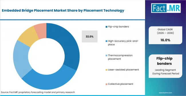
Embedded Bridge Placement Market Analysis By Placement Technology | Source: Fact.MR
Flip-chip bonders combine vision alignment, controlled force and thermal handling for placing a thin silicon bridge onto fine-pitch substrate features. The equipment already addresses many of the registration and contact requirements of advanced die attach. General high-accuracy pick-and-place systems offer flexibility, but they may lack the bond-force, temperature and process integration required for embedded bridge attachment. Finetech documents sub-micrometer placement capability, while K&S describes thermo-compression bonding with precise temperature, pressure and tilt control for fine-pitch advanced packaging. [2][3] Selection therefore depends on post-placement accuracy, controlled force, thermal handling and integration with the substrate process.
Why does <1 um lead Placement Accuracy?
<1 um is projected to account for 42.1% share in 2026.
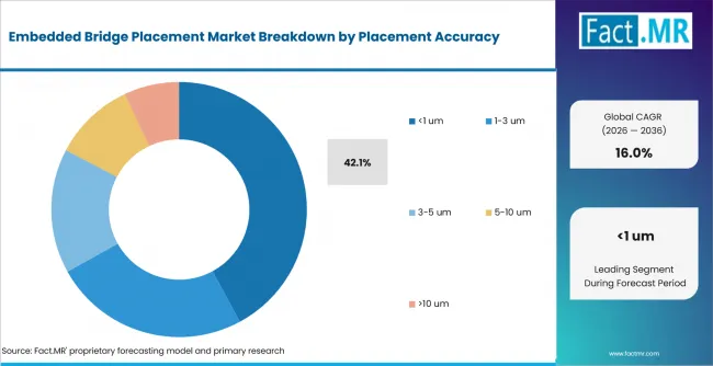
Embedded Bridge Placement Market Analysis By Placement Accuracy | Source: Fact.MR
Sub-micrometer placement protects overlap between bridge terminals and the surrounding build-up wiring after substrate distortion and lamination are included. It also preserves routing density at the localized high-bandwidth interface. The 1-3 micrometer class is easier to achieve but can consume too much of the alignment budget for the finest bridge designs. Intel's EMIB architecture embeds a small silicon bridge in the package substrate, concentrating fine-pitch routing where it is required. [1] Sub-micrometer placement therefore leads where fine bridge-pad pitch leaves little margin for substrate distortion or downstream alignment error.
Why do Silicon bridges lead Bridge Type?
Silicon bridges are projected to account for 46.5% share in 2026.
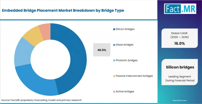
Embedded Bridge Placement Market Analysis By Bridge Type | Source: Fact.MR
Silicon bridges provide fine lithographic routing, mature microbump or hybrid interfaces and a thermal expansion behavior familiar to semiconductor assembly. They are the established route for localized high-density interconnect. Glass bridges can improve electrical or dimensional characteristics in selected designs, but their fabrication and attach ecosystem is less established. EMIB manufacturing: precise cavities are created in the laminate material where the silicon bridges will be placed. The small silicon bridges are then carefully placed into these cavities and are held in place with a specialized adhesive. [1] Silicon bridges remain the established choice because they combine localized fine-pitch routing with semiconductor-compatible fabrication.
Why does Organic panel lead Substrate Format?
Organic panel is projected to account for 44.2% share in 2026.
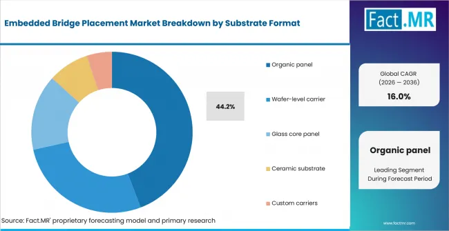
Embedded Bridge Placement Market Analysis By Substrate Format | Source: Fact.MR
Organic panels combine lower-cost package-substrate manufacturing with localized silicon bridges for dense die-to-die routing. Their larger work area can support multiple bridge placements per panel, but equipment must compensate for panel distortion and maintain repeatable cavity registration.
Why do OSAT providers lead End User?
OSAT providers are projected to account for 32.1% share in 2026.
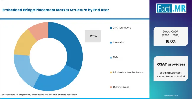
Embedded Bridge Placement Market Analysis By End User | Source: Fact.MR
OSAT providers integrate bridge placement with die attach, molding and package assembly and can optimize the sequence around customer package designs. Their equipment must switch between high-value, relatively low-volume product variants. Foundries participate in advanced packaging, but OSATs retain a broad installed base and customer mix for bridge-based assembly. Bridge placement error propagates into die attach: the die's fine-pitch microbumps must align to bridge pads while C4 bumps align to substrate pads - bridge placement tolerance is set by the finest bridge pad pitch, with TCB used at the finest pitches. [3] OSAT demand favors tools that support multiple package designs, traceable recipes and fast changeover without sacrificing placement accuracy.
What is accelerating Embedded Bridge Placement Market adoption, and what is holding it back?
The strongest accelerator is process position and precision class, while the main restraint is that bridge shift during adhesive cure or lamination can consume the placement margin after the tool has released the part.
Drivers Impact Analysis
| DRIVER | (~) % IMPACT ON CAGR | GEOGRAPHIC RELEVANCE | IMPACT TIMELINE |
|---|---|---|---|
| Process position and precision class | +4.5% | Global leading-edge fabs | Medium term (2-4 years) |
| Placement accuracy cascade | +3.7% | Global leading-edge fabs | Medium term (2-4 years) |
| Yield economics of placement | +3.0% | Global leading-edge fabs | Medium term (2-4 years) |
| Bond-process control | +2.4% | Global leading-edge fabs | Medium term (2-4 years) |
Source: Fact.MR analysis. Updated Jul 22, 2026
- Process position and precision class: Intel describes EMIB as a process in which bridges are placed into substrate cavities and secured with adhesive before dielectric and metal build-up. [1]
- Placement accuracy cascade: Bridge placement error propagates into die attach: the die's fine-pitch microbumps must align to bridge pads while C4 bumps align to substrate pads - bridge placement tolerance is set by the finest bridge pad pitch, with TCB used at the finest pitches. [3]
- Yield economics of placement: The localized bridge reduces the amount of fine-routing silicon, but the economic advantage depends on accurate cavity placement and high-yield substrate integration. [1]
- Bond-process control: Finetech documents 0.5 µm placement capability for the FINEPLACER sigma, while K&S emphasizes precise temperature, pressure and tilt control in thermo-compression bonding. [2][3]
Opportunity Impact Analysis
| OPPORTUNITY | (~) % IMPACT ON CAGR | GEOGRAPHIC RELEVANCE | IMPACT TIMELINE |
|---|---|---|---|
| Bridge proliferation raises placement throughput demand | +2.7% | Global leading-edge fabs | Short term (<=2 years) |
| Panel-scale embedding | +2.1% | Global leading-edge fabs | Medium term (2-4 years) |
| Adhesive-secured placement vs. self-assembly | +1.6% | Global leading-edge fabs | Short term (<=2 years) |
Source: Fact.MR analysis. Updated Jul 22, 2026
- Bridge proliferation raises placement throughput demand: Packages using more localized bridges increase the number of precision placement events and make cycle time, recipe control and automated handling more important.
- Panel-scale embedding: Larger organic panels can carry multiple bridge sites, creating demand for wide-field accuracy and compensation for panel distortion.
- Adhesive-secured placement: Intel documents bridges placed in substrate cavities and held with adhesive, making dispense control, placement stability and cure behavior part of equipment qualification. [1]
Restraints Impact Analysis
| RESTRAINT | (~) % IMPACT ON CAGR | GEOGRAPHIC RELEVANCE | IMPACT TIMELINE |
|---|---|---|---|
| Primary qualification constraint | -2.4% | Global leading-edge fabs | Medium term (2-4 years) |
| Process-window sensitivity | -1.9% | Global leading-edge fabs | Medium term (2-4 years) |
| Thermal and mechanical distortion | -1.4% | Global leading-edge fabs | Medium term (2-4 years) |
Source: Fact.MR analysis. Updated Jul 22, 2026
- Primary qualification constraint: Bridge shift during adhesive cure or dielectric build-up can consume placement margin after the tool releases the part.
- Process-window sensitivity: Cavity dimensions, adhesive volume, bridge thickness and substrate planarity must remain within a linked process window to preserve downstream alignment.
- Thermal and mechanical distortion: Panel warpage and cure-induced movement can alter bridge position, requiring compensation and post-embed metrology.
Which countries are scaling Embedded Bridge Placement Market fastest?
In USA, Embedded Bridge Placement Market is projected to advance at 17.6% CAGR, supported by leading-edge logic, high-performance computing, federally supported semiconductor R&D and a large domestic equipment base.
- Countries differ less by the headline CAGR than by the type of semiconductor work creating demand for the Embedded Bridge Placement Market.
- Taiwan follows a pathway shaped by leading foundry production, advanced packaging and a dense OSAT and substrate supply chain. USA takes a different path through leading-edge logic, high-performance computing, federally supported semiconductor R&D and a large domestic equipment base.
- South Korea remains aligned through distinct combinations of device production, equipment development and advanced packaging investment.
- Malaysia develops through large-scale outsourced assembly, test and package manufacturing, while Japan relies on semiconductor equipment, materials, inspection and memory-process expertise.
- Markets with similar CAGRs can follow different development paths because installed fabs, device mix, local equipment capability, export controls and qualification cycles differ.
The full report compares the five named country markets within the wider regional coverage of North America, Latin America, Europe, East Asia, South Asia & Oceania, and the Middle East & Africa.
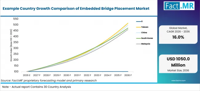
Example Country Growth Comparison Of Embedded Bridge Placement Market | Source: Fact.MR
| COUNTRY | CAGR 2026 to 2036 |
|---|---|
| Taiwan | 17.8% |
| USA | 17.6% |
| South Korea | 16.8% |
| Malaysia | 16.5% |
| Japan | 16.1% |
Source: Fact.MR analysis. Updated Jul 22, 2026
What is driving Taiwan's growth through 2036?
17.8% CAGR, supported by leading foundry production, advanced packaging and a dense OSAT and substrate supply chain.
Taiwan's foundry, OSAT and substrate ecosystem supports qualification of high-accuracy placement and bonding equipment for advanced multi-die packages.
What is driving USA's growth through 2036?
17.6% CAGR, supported by leading-edge logic, high-performance computing, federally supported semiconductor R&D and a large domestic equipment base.
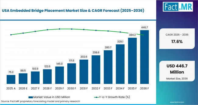
Embedded Bridge Placement Market Country Value Analysis | Source: Fact.MR
Intel's production-proven EMIB architecture and the country's advanced-packaging investment base support demand for precise bridge-placement and substrate-integration equipment. [1]
What is driving South Korea's growth through 2036?
16.8% CAGR, supported by high-volume memory, HBM and vertically integrated semiconductor manufacturing.
South Korea's memory and vertically integrated semiconductor manufacturing base supports advanced-packaging equipment qualification for dense multi-die assemblies.
What is driving Malaysia's growth through 2036?
16.5% CAGR, supported by large-scale outsourced assembly, test and package manufacturing.
Malaysia combines large-scale outsourced assembly, test and package manufacturing with a 12.4% share of 2026 demand across the five profiled countries. Intel's documented EMIB flow places bridges into substrate cavities before dielectric and metal build-up layers are added. [1] The commercial link is the need to solve the problem of placing small silicon or glass bridges into substrate cavities with micron-class registration and controlled planarity as capacity and process complexity increase.
What is driving Japan's growth through 2036?
16.1% CAGR, supported by semiconductor equipment, materials, inspection and memory-process expertise.
Japan's substrate, materials and semiconductor-equipment base supports precision placement, bonding and process-control requirements for advanced packaging.
Who leads the Embedded Bridge Placement Market?
ASMPT and BESI lead the competitive landscape, followed by Kulicke & Soffa and Shinkawa as the next tier of challengers.
ASMPT supplies advanced-packaging platforms for die and flip-chip bonding, thermo-compression bonding and embedded-package applications. [4]
Besi provides high-accuracy die-placement and hybrid-bonding platforms for dense interconnect and 3D integration. [5]
Kulicke & Soffa supplies thermo-compression bonding systems with controlled heat, pressure and tilt for fine-pitch advanced packaging. [3]
Yamaha Robotics markets SHINKAWA Series semiconductor bonding equipment, including precision die-bonding platforms. [6]
Palomar Technologies provides precision die-attach systems for microelectronic and specialty-packaging applications. [7]
Panasonic Connect supplies die and flip-chip bonders for high-accuracy semiconductor assembly. [8]
Competition is expected to center on repeatable process performance, integration with adjacent modules, installed-base service and documented capability to address the challenge of placing small silicon or glass bridges into substrate cavities with micron-class registration and controlled planarity. Buyers are likely to compare accuracy, defect prevention, throughput, recipe stability and the completeness of the delivered process cell.
Which companies are the key providers?
Key companies include ASMPT; BESI; Kulicke & Soffa; Shinkawa; Palomar Technologies; Panasonic.
- ASMPT
- BESI
- Kulicke & Soffa
- Shinkawa
- Palomar Technologies
- Panasonic
Bibliography
- [1] Intel Foundry. (2025). EMIB Technology Brief. https://www.intel.com/content/dam/www/central-libraries/us/en/documents/2025-07/emib-product-brief.pdf
- [2] Finetech. FINEPLACER sigma Advanced Sub-Micron Bonder. https://de.finetech.de/wp-content/uploads/2022/11/Technical-Data-Sheet_sigma_rev2.2.2_EN_web-1.pdf?download=1
- [3] Kulicke & Soffa. Thermo-Compression Bonding. https://www.kns.com/products-services/thermo-compression-bonding
- [4] ASMPT. Advanced Packaging Solutions. https://semi.asmpt.com/en/products/ap/
- [5] Besi. Hybrid Bonding. https://www.besi.com/products-technology/product-details/productgroup/hybrid-bonding/
- [6] Yamaha Robotics. SHINKAWA Series. https://www.yamaha-robotics.com/en/brand/shinkawa
- [7] Palomar Technologies. Precision Die Attach Placement Accuracy. https://www.palomartechnologies.com/news-room/press-releases/bid/106056/palomar-technologies-presents-sub-5um-die-attach-placement-accuracy-webcast
- [8] Panasonic Connect. MD-P300 Flip-chip Bonder. https://ap.connect.panasonic.com/sg/en/md-p300-flip-chip-bonder
This Report Addresses
- The report provides strategic intelligence on Embedded Bridge Placement Market across Placement Technology and Placement Accuracy choices that shape purchasing decisions.
- Segment analysis covers Flip-chip bonders as the share leader within the 2026 market structure.
- Regional outlook evaluates Taiwan alongside South Korea and Malaysia, while USA and Japan complete the growth comparison.
- Competitive analysis profiles ASMPT and BESI alongside Kulicke & Soffa and Shinkawa, followed by additional active providers.
- Use-case assessment covers the categories and applications that shape demand in the Embedded Bridge Placement Market across the forecast period.
What does the Embedded Bridge Placement Market cover?
The market covers equipment and process systems configured to address the challenge of placing small silicon or glass bridges into substrate cavities with micron-class registration and controlled planarity.
Embedded bridge placement equipment places small silicon bridge dies into cavities in organic (or glass) package substrates with micron-level accuracy before build-up lamination - the bridge embedding step of EMIB-class flows. The segment sits between die bonding and substrate fabrication: placement happens in laminate substrate fabs, not wafer fabs, at panel scale, with the bridge held by adhesive and then buried.
Commercial value arises from the complete configured system, including process control, handling, software and integrated modules required for repeatable operation. Finished semiconductor devices, package value and unrelated parent-market equipment are excluded.
What is included in the scope?
The scope includes systems used by osat providers and the other end-user groups listed in the segmentation.
The market is segmented by Placement Technology, including Flip-chip bonders, High-accuracy pick-and-place, Thermocompression placement, Laser-assisted placement, Collective placement; Placement Accuracy, including <1 um, 1-3 um, 3-5 um, 5-10 um, >10 um; Bridge Type, including Silicon bridges, Glass bridges, Photonic bridges, Passive interconnect bridges, Active bridges; Substrate Format, including Organic panel, Wafer-level carrier, Glass core panel, Ceramic substrate, Custom carriers; End User, including OSAT providers, Foundries, IDMs, Substrate manufacturers, R&D institutes.
Integrated handling, metrology, cleaning, activation, process-control or support modules are included when delivered as part of the configured market system.
What is excluded from the scope?
The scope excludes unrelated semiconductor equipment, standalone materials and components sold independently of the configured system.
It also excludes facility construction, cleanroom infrastructure, the value of processed wafers or packages, and adjacent process steps that are not part of the defined equipment category.
How Was the Analysis Built?
Fact.MR is of the opinion that this assessment combines structured market analysis with a review of public information and industry evidence relevant to the market.
- Market Assessment: The analysis considers demand patterns, supply conditions, segment mix, country activity, company participation, and adoption trends.
- Evidence Review: Public company disclosures, government and regulatory publications, trade information, technical literature, and industry records inform the assessment.
- Validation and Updates: Findings are cross-checked against available market indicators and reviewed when material market developments emerge.
Segmentation
What is the report's scope and coverage?
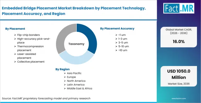
Embedded Bridge Placement Market Breakdown By Placement Technology, Placement Accuracy, And Region | Source: Fact.MR
| Attribute | Details |
|---|---|
| Quantitative Units | USD Million in 2026 to USD Million by 2036 at a CAGR |
| Market Definition | Embedded bridge placement equipment places small silicon bridge dies into cavities in organic (or glass) package substrates with micron-level accuracy before build-up lamination - the bridge embedding step of EMIB-class flows. The segment sits between die bonding and substrate fabrication: placement happens in laminate substrate fabs, not wafer fabs, at panel scale, with the bridge held by adhesive and then buried. |
| Placement Technology | Flip-chip bonders; High-accuracy pick-and-place; Thermocompression placement; Laser-assisted placement; Collective placement |
| Placement Accuracy | <1 um; 1-3 um; 3-5 um; 5-10 um; >10 um |
| Bridge Type | Silicon bridges; Glass bridges; Photonic bridges; Passive interconnect bridges; Active bridges |
| Substrate Format | Organic panel; Wafer-level carrier; Glass core panel; Ceramic substrate; Custom carriers |
| End User | OSAT providers; Foundries; IDMs; Substrate manufacturers; R&D institutes |
| Regions Covered | North America; Latin America; Europe; East Asia; South Asia & Oceania; Middle East & Africa |
| Countries Covered | Taiwan; South Korea; Malaysia; USA; Japan |
| Key Companies Profiled | ASMPT; BESI; Kulicke & Soffa; Shinkawa; Palomar Technologies; Panasonic |
| Forecast Period | 2026 to 2036 |
| Approach | Hybrid top-down and bottom-up approach using demand indicators across Placement Technology; Placement Accuracy; Bridge Type; Substrate Format; End User; country-level growth; company participation and adoption trends |
Source: Fact.MR analysis. Updated Jul 22, 2026
How is the market segmented?
-
By Placement Technology:
- Flip-chip bonders
- High-accuracy pick-and-place
- Thermocompression placement
- Laser-assisted placement
- Collective placement
-
By Placement Accuracy:
- <1 um
- 1-3 um
- 3-5 um
- 5-10 um
- >10 um
-
By Bridge Type:
- Silicon bridges
- Glass bridges
- Photonic bridges
- Passive interconnect bridges
- Active bridges
-
By Substrate Format:
- Organic panel
- Wafer-level carrier
- Glass core panel
- Ceramic substrate
- Custom carriers
-
By End User:
- OSAT providers
- Foundries
- IDMs
- Substrate manufacturers
- R&D institutes
-
By Region:
- North America
- Latin America
- Europe
- East Asia
- South Asia & Oceania
- Middle East & Afric
Frequently Asked Questions
Which Placement Technology leads the Embedded Bridge Placement Market?
Which Placement Accuracy leads the Embedded Bridge Placement Market?
Which Bridge Type leads the Embedded Bridge Placement Market?
Which Substrate Format leads the Embedded Bridge Placement Market?
Which End User leads the Embedded Bridge Placement Market?
What CAGR is projected for Taiwan in the Embedded Bridge Placement Market?
What CAGR is projected for USA in the Embedded Bridge Placement Market?
What CAGR is projected for China in the Embedded Bridge Placement Market?
What CAGR is projected for South Korea in the Embedded Bridge Placement Market?
What CAGR is projected for Malaysia in the Embedded Bridge Placement Market?
What CAGR is projected for Japan in the Embedded Bridge Placement Market?
What is the primary driver of the Embedded Bridge Placement Market?
What is the main restraint in the Embedded Bridge Placement Market?
Who worked on this report


Preview the report firsthand - request a free sample
Free SampleGet the brochure for pricing and purchase details
Download PDF