- Market Value (2025): USD 1.4 Bn
- Estimated Value (2026): USD 1.6 Bn
- Forecast Value (2036): USD 7.8 Bn
- CAGR (2026-2036): 17.1%
What is the HBM Known Good Die KGD Screening and Test Market forecast to be worth by 2036?
USD 1.6 billion in 2026 to USD 7.8 billion by 2036 at 17.1% CAGR.
- The HBM known good die KGD screening and test market crossed a valuation of USD 1.4 billion in 2025.
- Demand is projected to increase from USD 1.6 billion in 2026 to USD 7.8 billion by 2036.
- The market is forecast to expand at 17.1% CAGR from 2026 to 2036.
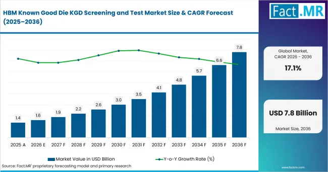
Hbm Known Good Die Kgd Screening And Test Market Value Analysis | Source: Fact.MR
What are the defining numbers behind HBM Known Good Die KGD Screening and Test Market growth?
USD 6.2 billion absolute opportunity by 2036.
- Demand Drivers in the Market
- AI training and inference hardware is expected to raise demand for HBM screening because data center accelerator platforms need reliable memory stacks before system release.
- Chiplet design and 3D semiconductor packaging are anticipated to make earlier die acceptance more useful since failed parts are harder to recover after stacking. In January 2025, the U.S. Department of Commerce finalized $1.4 billion under the CHIPS NAPMP to boost domestic advanced packaging. However, following structural reviews later that year, the $1.1 billion operational contract originally awarded to Natcast was halted, shifting direct oversight of the advanced packaging facilities to NIST
- HBM stack inspection is expected to support buyer confidence where memory stacks move from package qualification into higher volume production.
- Key Segments Analyzed
- By Test Solution: Known Good Die Screening is expected to hold 54.0% share in 2026 because early die acceptance lowers downstream package risk.
- By Application: HBM3E Memory Validation is projected to account for 46.0% share in 2026 as buyers qualify faster memory for AI processors.
- By End User: Memory Manufacturers are anticipated to represent 44.0% share in 2026 due to their direct control over HBM die output.
- By Test Deployment: Wafer-level Testing is estimated to hold 59.0% share in 2026 because screening before dicing protects later assembly yield.
- By Test Technology: Wafer Probe Testing is forecast to capture 52.0% share in 2026 since probe workflows remain central to die qualification.
- Analyst Opinion at Fact.MR
- Shambhu Nath Jha, Senior Consultant at Fact.MR, states, “HBM KGD screening is moving closer to the economics of advanced packaging. Buyers judge test equipment by early weak-die isolation and stable heat control. They need results that transfer into high-yield stack assembly.”
- Strategic Implications
- Test-equipment suppliers should show how wafer probe results guide stack-level quality decisions so memory manufacturers can shorten qualification cycles.
- Firms serving advanced IC substrates can strengthen customer discussions by connecting substrate readiness with probe access and thermal behavior.
- Vendors should deepen work with foundries and OSAT providers because HBM screening decisions often fall between memory output and final package assembly.
South Korea leads at 18.0% CAGR through memory manufacturing leadership. Taiwan follows at 17.5% as foundry scale supports advanced packaging and validation. The USA records 16.9% through CHIPS Act investments and AI infrastructure buildout. Japan reaches 16.3% through advanced materials and equipment supply chains. China posts 15.7% through domestic semiconductor programs. Germany records 15.1% through automotive semiconductor demand. Singapore reaches 14.4% through regional packaging and distribution roles.
How does the HBM Known Good Die KGD Screening and Test Market break down by segment?
Known Good Die Screening is expected to lead Test Solution at 54.0% share in 2026. HBM3E Memory Validation is projected to lead Application at 46.0% share in 2026.
Why does Known Good Die Screening lead Test Solution?
Known Good Die Screening is projected to account for 54.0% share in 2026.
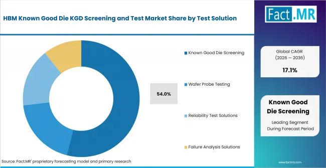
Hbm Known Good Die Kgd Screening And Test Market Analysis By Test Solution | Source: Fact.MR
This sub-segment leads because HBM packages carry high assembly value before final system testing begins. Memory suppliers need early proof that each die can enter a stack. The screening step reduces the chance that a weak die moves into an expensive package build.
Why does HBM3E Memory Validation lead Application?
HBM3E Memory Validation leads with 46.0% share in 2026.
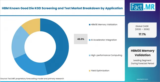
Hbm Known Good Die Kgd Screening And Test Market Analysis By Application | Source: Fact.MR
HBM3E validation is central to the market since AI accelerators need fast memory with stable electrical behavior. Buyers use validation results to confirm speed and thermal response before pairing memory with processors. This makes the application a leading spending area in the base year. In March 2025, Micron announced that HBM3E 12H 36GB was designed into NVIDIA HGX B300 NVL16 and GB300 NVL72 platforms, keeping qualification pressure high around AI memory.
Why do Memory Manufacturers lead End User?
Memory Manufacturers are projected to account for 44.0% share in 2026.
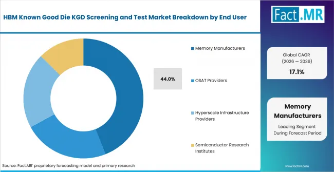
Hbm Known Good Die Kgd Screening And Test Market Analysis By End User | Source: Fact.MR
Memory manufacturers lead end-user demand because they control die output before HBM stacks reach packaging. Their test choices affect binning and shipment readiness. Strong screening capability helps reduce late-stage failures after high-value dies have entered stacked formats. In September 2025, SK hynix said it completed HBM4 development and prepared mass production, with bandwidth doubled and power efficiency improved by more than 40% compared with the previous generation.
What supports Wafer-level Testing within Test Deployment?
Wafer-level Testing holds 59.0% share in 2026.
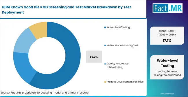
Hbm Known Good Die Kgd Screening And Test Market Analysis By Test Deployment | Source: Fact.MR
Wafer-level testing holds the lead by giving manufacturers earlier visibility into die quality. Testing at this stage supports faster sorting before dicing and package build. For HBM, each rejected weak die can protect later stacking yield.
What supports Wafer Probe Testing within Test Technology?
Wafer Probe Testing is projected to account for 52.0% share in 2026.
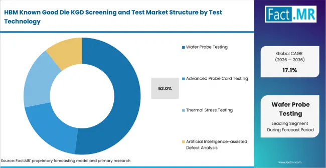
Hbm Known Good Die Kgd Screening And Test Market Analysis By Test Technology | Source: Fact.MR
Wafer probe testing remains the leading technology because it connects die-level electrical results with production release decisions. Probe cards and automated test systems must handle dense contact patterns during HBM qualification. The workflow stays useful as memory speeds rise.
What is accelerating HBM Known Good Die KGD Screening and Test Market adoption, and what is holding it back?
Demand is expected to rise as AI processors and HBM stacks require stricter die-level screening before advanced assembly. Growth may be limited by capital intensity and the engineering time needed to qualify new test workflows for AI server chassis platforms.
Drivers Impact Analysis
| DRIVER | IMPACT ON CAGR | GEOGRAPHIC RELEVANCE | IMPACT TIMELINE |
|---|---|---|---|
| Technology Innovation & R&D | High | Global | 2026-2036 |
| Regulatory & Policy Drivers | Medium-High | North America, Europe | 2026-2032 |
| End-User Industry Expansion | High | Asia Pacific, MEA | 2026-2036 |
| Operational & Cost Efficiency | Medium | Global | 2026-2036 |
Source: Fact.MR analysis. Updated Aug 11, 2026
- Technology Innovation & R&D: Higher memory speed and tighter thermal limits are expected to raise the value of probe accuracy and screening repeatability.
- Regulatory & Policy Drivers: Regional semiconductor investment programs are anticipated to support test infrastructure where fabs and packaging sites add local capacity. In January 2025, NIST said SMART USA received USD 285 million to use digital twins for semiconductor design, manufacturing, advanced packaging, assembly, and test processes.
- End-User Industry Expansion: AI computing and high-performance data centers are forecast to widen the buyer base for HBM screening equipment.
Opportunity Impact Analysis
| OPPORTUNITY | IMPACT ON CAGR | GEOGRAPHIC RELEVANCE | IMPACT TIMELINE |
|---|---|---|---|
| HBM burn-in and screening integration | Medium-High | South Korea, Taiwan, USA | 2026-2032 |
| Thermal-aware die probing | Medium | Advanced memory fabs | 2026-2036 |
| Test data transfer into advanced packaging | Medium | Memory and OSAT clusters | 2026-2036 |
| Automotive and defense compute qualification | Low-Medium | USA, Japan, Germany | 2028-2036 |
Source: Fact.MR analysis. Updated Aug 11, 2026
- HBM burn-in and screening integration: Suppliers that connect die screening with later reliability checks are expected to gain acceptance from memory manufacturers.
- Thermal-aware die probing: Probing systems that preserve stable temperature conditions are anticipated to become more valuable as data center server rack power density rises.
- Test data transfer into advanced packaging: Buyers are expected to favor systems that make die-level results usable during package qualification.
Restraints Impact Analysis
| RESTRAINT | IMPACT ON CAGR | GEOGRAPHIC RELEVANCE | IMPACT TIMELINE |
|---|---|---|---|
| Capital Intensity & Investment | Medium | Developing Markets | 2026-2030 |
| Supply Chain & Raw Material | Medium | Global | 2026-2028 |
| Workforce & Capability Gaps | Low-Medium | Africa, Latin America | 2026-2036 |
| Thermal and signal-integrity control | Medium | Advanced memory fabs | 2026-2032 |
Source: Fact.MR analysis. Updated Aug 11, 2026
- Capital Intensity & Investment: HBM screening requires advanced probers and test platforms that can be costly for smaller facilities.
- Supply Chain & Raw Material: Long lead times for precision components can delay tool installation and extend qualification schedules.
- Workforce & Capability Gaps: Skilled process and test engineers are needed to interpret HBM screening results and transfer them into production decisions.
Which countries are scaling the HBM Known Good Die KGD Screening and Test Market fastest?
- South Korea remains 0.5 percentage point above Taiwan through memory manufacturing leadership.
- Taiwan remains 0.6 percentage point above the USA where foundry depth supports advanced packaging validation.
- The USA remains 0.6 percentage point above Japan through CHIPS Act investment and AI infrastructure buildout.
- Japan remains 0.6 percentage point above China due to advanced materials and equipment supply-chain strength.
- China remains 0.6 percentage point above Germany through domestic semiconductor self-sufficiency initiatives.
- Germany remains 0.7 percentage point above Singapore as automotive semiconductor demand supports local qualification work.
- Singapore closes the displayed range through advanced packaging support and regional distribution.
Comparable CAGRs can create different entry conditions because each country has a different mix of memory output and package assembly depth. Full report coverage includes North America; Latin America; Europe; Asia Pacific; Middle East and Africa.
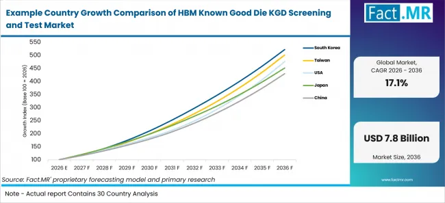
Example Country Growth Comparison Of Hbm Known Good Die Kgd Screening And Test Market | Source: Fact.MR
| Country | CAGR (2026-2036) |
|---|---|
| South Korea | 18.0% |
| Taiwan | 17.5% |
| USA | 16.9% |
| Japan | 16.3% |
| China | 15.7% |
| Germany | 15.1% |
| Singapore | 14.4% |
Source: Fact.MR analysis. Updated Aug 11, 2026
What is driving the HBM Known Good Die KGD Screening and Test market in South Korea?
18.0% CAGR, supported by memory manufacturing leadership.
South Korea is expected to stay the fastest listed market because HBM screening fits directly into its memory production base. Local demand is concentrated near die output and stack qualification. Equipment buyers are expected to value tools that help weak dies get removed before package value rises. In June 2026, the U.S. International Trade Administration reported that South Korea's semiconductor exports reached USD 173.4 billion in 2025, up 22.2% and equal to about 24.4% of total exports.
How is Taiwan scaling demand?
17.5% CAGR, driven by its dominant semiconductor foundry ecosystem.
Taiwan’s demand is shaped by foundry scale and close packaging coordination. Buyers are expected to need KGD screening where dies move quickly from wafer testing into advanced assembly. The local mechanism is practical: better die-level evidence can reduce risk before integration.
What supports USA adoption?
16.9% CAGR, backed by CHIPS Act investments and AI infrastructure buildout.
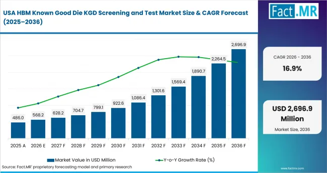
Hbm Known Good Die Kgd Screening And Test Market Country Value Analysis | Source: Fact.MR
The USA is expected to gain from advanced computing investment and renewed semiconductor capacity planning. Test buyers are likely to prioritize traceability and reliability data. Those needs matter because HBM failures can affect expensive accelerator modules late in the release path. NIST reported a supplemental CHIPS award of up to USD 75 million for GlobalFoundries' Malta facility to support advanced packaging, chiplet integration, and wafer-to-wafer hybrid bonding.
How does Japan perform?
16.3% CAGR, led by advanced materials and equipment supply-chain strength.
Japan’s growth reflects its position in precision semiconductor equipment and material support. Local test demand is expected to favor stable probing and thermal handling. These capabilities matter when HBM validation must remain repeatable across different device lots.
What is driving China’s growth from 2026 to 2036?
15.7% CAGR, supported by domestic semiconductor self-sufficiency initiatives.
China’s market is expected to expand where local semiconductor programs need more control over testing and qualification. Screening demand is tied to domestic tool use and engineering support. The market may still face slower qualification where equipment access remains difficult. China's State Council cited Ministry of Industry and Information Technology data showing integrated-circuit output reached 484.3 billion units in 2025, up 10.9% year over year.
What supports Germany’s demand?
15.1% CAGR, driven by automotive semiconductor and industrial IoT demand.
Germany’s demand is expected to come from advanced electronics used in vehicles and industrial systems. HBM KGD screening has a narrower role here than in memory-led Asian markets. The opportunity is strongest where reliable high-performance modules support compute-heavy applications.
How is Singapore developing demand?
14.4% CAGR, supported by advanced packaging and regional distribution.
Singapore is expected to develop demand through semiconductor services and regional packaging support. Its compact production cluster can support qualification work close to electronics supply chains. Buyers are likely to favor screening workflows that help package release and customer approval.
Who leads the HBM Known Good Die KGD Screening and Test Market?
Advantest Corporation; Teradyne, Inc.; and FormFactor, Inc. show the clearest direct relevance to HBM KGD screening and test. Technoprobe S.p.A.; Tokyo Electron Limited; Cohu, Inc.; MPI Corporation extend the competitive field across probe cards and memory validation workflows.
Competition is shaped by qualification depth instead of product breadth alone. Advantest said in August 2025 that it would feature end-to-end memory test solutions for HBM and other memory devices. Teradyne released Magnum 7H in August 2025 for high bandwidth memory devices used with GPUs and accelerators. FormFactor published in February 2025 that KGD wafer test work addresses electrical and thermal challenges for next-generation memory devices. Tokyo Electron released Prexa SDP in April 2026 for singulated device testing and accurate KGD selection.
Which companies are the key providers?
Key companies profiled in the HBM Known Good Die KGD Screening and Test market include Advantest Corporation; Teradyne, Inc.; FormFactor, Inc.; Technoprobe S.p.A.; Tokyo Electron Limited; Cohu, Inc.; MPI Corporation.
- Advantest Corporation
- Teradyne, Inc.
- FormFactor, Inc.
- Technoprobe S.p.A.
- Tokyo Electron Limited
- Cohu, Inc.
- MPI Corporation
Bibliography
- Advantest Corporation. (2025, August 4). Advantest will Showcase Latest Memory Test Solutions at Future of Memory and Storage 2025.
- FormFactor, Inc. (2025, February 21). High-Speed Test Solutions for Known Good Die Wafer Test on Memory ICs.
- SEMI. (2026, April 7). SEMI Reports Global Semiconductor Equipment Billings Reached $135 Billion in 2025, Up 15% Year-on-Year.
- Teradyne, Inc. (2025, August 4). Teradyne Unveils Magnum 7H - The Next-Generation Memory Tester for High Bandwidth Memory Devices.
- Tokyo Electron Limited. (2026, April 16). Tokyo Electron Releases Prexa™ SDP, a New Device Prober.
- Cohu, Inc. (2025, September 16). Cohu Secures Additional Neon Orders, Raises 2025 Forecasted HBM Revenue to $10-$11 million.
- International Trade Administration. (2026, June 29). Korea - Digital Economy.
- Micron Technology, Inc. (2025, March 18). Micron Innovates From the Data Center to the Edge With NVIDIA.
- National Institute of Standards and Technology. (2025, January 3). Biden-Harris Administration Awards Semiconductor Research Corporation Manufacturing Consortium Corporation $285M for New CHIPS Manufacturing USA Institute for Digital Twins, Headquartered in North Carolina.
- National Institute of Standards and Technology. (2025, January 16). U.S. Department of Commerce Announces $1.4 Billion in Final Awards to Support the Next Generation of U.S. Semiconductor Advanced Packaging.
- National Institute of Standards and Technology. (2025, January 17). U.S. Department of Commerce Announces CHIPS Incentives Awards with Corning, Edwards Vacuum, and Infinera to Increase Domestic Production Capacity of Chips and Equipment Critical for U.S. Technological Leadership.
- SK hynix Inc. (2025, September 12). SK hynix Completes World's First HBM4 Development and Readies Mass Production.
This Report Answers
- The report provides strategic intelligence on the HBM Known Good Die KGD Screening and Test Market across Test Solution and Application choices that shape memory qualification.
- Segment analysis covers Known Good Die Screening and HBM3E Memory Validation as the share leaders within the 2026 market.
- Country outlook evaluates South Korea and Taiwan alongside the USA and Japan. China and Germany complete the growth comparison with Singapore.
- Competitive analysis profiles Advantest Corporation and Teradyne, Inc. alongside FormFactor, Inc. and Tokyo Electron Limited.
- Process assessment covers Wafer-level Testing and Wafer Probe Testing. These workflows shape the release path before advanced packaging.
What does the HBM Known Good Die KGD Screening and Test Market cover?
HBM KGD screening covers test workflows that confirm die quality before memory is stacked or integrated into high-value packages. The market includes electrical and thermal checks at wafer or die level. Reliability evidence guides release decisions.
Coverage extends to HBM3E memory validation and workflows used around 3D TSV packages. The market also considers test data that supports advanced package yield and customer acceptance. It does not include general semiconductor testing unless the activity is directly tied to HBM die qualification.
What is included in the scope?
The scope includes Test Solution; Application; End User; Test Deployment; Test Technology. Coverage spans Known Good Die Screening and HBM3E Memory Validation. It includes Memory Manufacturers and Wafer-level Testing alongside Wafer Probe Testing.
Adjacent context includes queue-time hybrid bonders where package timing affects the value of earlier die screening. The scope also considers how test data moves into package qualification and customer release workflows.
What is excluded from the scope?
The scope excludes company market-share estimates and revenue allocation by vendor. It also excludes unrelated semiconductor equipment categories and generic inspection tools that do not support HBM die release.
General packaging spending and broad memory-device revenue are outside the scope unless they directly affect KGD screening demand. Product pages without dated evidence are not treated as company developments.
How Was the Analysis Built?
The analysis draws on 120+ sources, 35+ company portfolios, 25+ countries, and more than 20 industry interviews.
- Primary Research: Primary research includes discussions with manufacturers, service providers, technology developers, distributors, end users, procurement teams, and subject-matter experts. These conversations examine purchasing priorities, product adoption, operational challenges, approval requirements, competitive positioning, and the factors that influence wider market acceptance.
- Desk Research: Desk research covers government statistics, regulatory publications, company filings, trade data, technical studies, industry associations, standards, public policy, and other authoritative sources. Every source used in the analysis is documented in the bibliography.
- Market Sizing and Forecasting: Market estimates combine historical performance, demand indicators, pricing and volume trends, segment shares, company participation, country-level growth, adoption patterns, investment activity, and barriers to market expansion.
- Data Validation and Update Cycle: Findings are validated by comparing primary interviews with public data, company activity, regulatory changes, trade patterns, and industry developments. Regular updates review new product launches, capacity changes, partnerships, approvals, procurement trends, and shifts in commercial adoption.
Segmentation
What is the report’s scope and coverage?
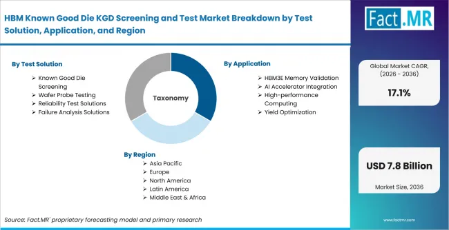
Hbm Known Good Die Kgd Screening And Test Market Breakdown By Test Solution, Application, And Region | Source: Fact.MR
| Attribute | Details |
|---|---|
| Quantitative Units | USD billion in 2026 to USD billion by 2036 at CAGR |
| Market Definition | Wafer-level and die-level screening used to confirm that HBM dies and related stacked memory components meet electrical, thermal, and reliability requirements before advanced packaging and system integration |
| Test Solution | Known Good Die Screening; Wafer Probe Testing; Reliability Test Solutions; Failure Analysis Solutions |
| Application | HBM3E Memory Validation; AI Accelerator Integration; High-performance Computing; Yield Optimization |
| End User | Memory Manufacturers; OSAT Providers; Hyperscale Infrastructure Providers; Semiconductor Research Institutes |
| Test Deployment | Wafer-level Testing; In-line Manufacturing Test; Quality Assurance Laboratories; Process Development Facilities |
| Test Technology | Wafer Probe Testing; Advanced Probe Card Testing; Thermal Stress Testing; Artificial Intelligence-assisted Defect Analysis |
| Regions Covered | North America; Europe; Asia Pacific; Latin America; Middle East & Africa |
| Countries Covered | South Korea; Taiwan; USA; Japan; China; Germany; Singapore |
| Key Companies Profiled | Advantest Corporation; Teradyne, Inc.; FormFactor, Inc.; Technoprobe S.p.A.; Tokyo Electron Limited; Cohu, Inc.; MPI Corporation |
| Forecast Period | 2026 to 2036 |
| Approach | Hybrid top-down and bottom-up approach using HBM screening demand; wafer-level and die-level qualification requirements; Known Good Die acceptance; HBM3E memory validation activity; wafer probe testing; electrical and thermal reliability checks; advanced packaging yield requirements; memory manufacturer and OSAT demand; test equipment adoption; AI accelerator integration; country growth patterns and company portfolio review. |
Source: Fact.MR analysis. Updated Aug 11, 2026
How is the market segmented?
-
By Test Solution
- Known Good Die Screening
- Pre-bond KGD Screening
- Post-bond KGD Screening
- Wafer Probe Testing
- High-bandwidth Memory Probe
- Burn-in Wafer Testing
- Reliability Test Solutions
- Thermal Cycling Test
- Electrical Reliability Test
- Failure Analysis Solutions
- Non-destructive Failure Analysis
- Physical Failure Analysis
- Known Good Die Screening
-
By Application
- HBM3E Memory Validation
- HBM3E Qualification
- HBM4 Development
- AI Accelerator Integration
- GPU Packaging Validation
- Chiplet Integration
- High-performance Computing
- Server Processor Validation
- Networking ASIC Validation
- Yield Optimization
- Process Improvement
- Defect Root Cause Analysis
- HBM3E Memory Validation
-
By End User
- Memory Manufacturers
- DRAM Manufacturers
- Logic Chip Manufacturers
- OSAT Providers
- Semiconductor Foundries
- Advanced Packaging Companies
- Hyperscale Infrastructure Providers
- Cloud Computing Companies
- Network Equipment Manufacturers
- Semiconductor Research Institutes
- Academic Research Centers
- Government Semiconductor Laboratories
- Memory Manufacturers
-
By Test Deployment
- Wafer-level Testing
- Pre-assembly Testing
- Final Test Operations
- In-line Manufacturing Test
- Production Test Lines
- Automated Test Facilities
- Quality Assurance Laboratories
- Reliability Qualification Centers
- Engineering Validation Labs
- Process Development Facilities
- Pilot Production Lines
- Reliability Engineering Labs
- Wafer-level Testing
-
By Test Technology
- Wafer Probe Testing
- High-speed Wafer Probing
- Known Good Die Characterization
- Advanced Probe Card Testing
- High-density Probe Card Technology
- Wafer Burn-in Technology
- Thermal Stress Testing
- High-temperature Reliability Test
- Electrical Parametric Testing
- Artificial Intelligence-assisted Defect Analysis
- X-ray Defect Inspection
- Focused Ion Beam Analysis
- Wafer Probe Testing
-
By Region
- North America
- Latin America
- Western Europe
- Eastern Europe
- East Asia
- South Asia and Pacific
- Middle East & Africa
Frequently Asked Questions
How big is the HBM Known Good Die KGD screening and test market in 2026?
What is the CAGR of the HBM Known Good Die KGD screening and test market from 2026 to 2036?
Which test solution leads the HBM Known Good Die KGD screening and test market?
Which application leads the HBM Known Good Die KGD screening and test market?
Who are the leading companies in the HBM Known Good Die KGD screening and test market?
Who worked on this report


Preview the report firsthand - request a free sample
Free SampleGet the brochure for pricing and purchase details
Download PDF