Organic Substrate Packaging Material Market Size, Share, Growth and Forecast (2025 - 2035)
Organic Substrate Packaging Material Market Size and Share Forecast Outlook 2025 to 2035
Organic substrate packaging material market is projected to grow from USD 16.9 billion in 2025 to USD 28.8 billion by 2035, at a CAGR of 5.5%. SO packages will dominate with a 41.0% market share, while consumer electronics will lead the application segment with a 45.0% share.
Organic Substrate Packaging Material Market Forecast and Outlook 2025 to 2035
The global organic substrate packaging material market is projected to grow from USD 16.9 billion in 2025 to approximately USD 28.8 billion by 2035, recording an extraordinary absolute increase of USD 11.9 billion over the forecast period. This translates into a total growth of 70.6%, with the market forecast to expand at a compound annual growth rate (CAGR) of 5.5% between 2025 and 2035.
The overall market size is expected to grow by over 1.7X during this period, supported by exponential demand for advanced semiconductor packaging solutions, rising adoption of high-density interconnect technologies, and growing emphasis on miniaturization innovation and electronic device performance optimization across global semiconductor operations.
Quick Stats on Organic Substrate Packaging Material Market
- Organic Substrate Packaging Material Market Value (2025): USD 16.9 billion
- Organic Substrate Packaging Material Market Forecast Value (2035): USD 28.8 billion
- Organic Substrate Packaging Material Market Forecast CAGR (2025 to 2035): 5.5%
- Leading Technology in Organic Substrate Packaging Material Market: SO packages (41.0%)
- Leading Application in Organic Substrate Packaging Material Market: Consumer Electronics (45.0%)
- Key Growth Regions in Organic Substrate Packaging Material Market: Asia Pacific, North America, and Europe
- Key Players in Organic Substrate Packaging Material Market: Amkor Technology Inc., Kyocera Corporation, Microchip Technology Inc., Texas Instruments Incorporated, ASE Kaohsiung, Simmtech Co., Ltd, Shinko Electric Industries Co. Ltd, LG Innotek Co. Ltd, AT&S, Daeduck Electronics Co. Ltd
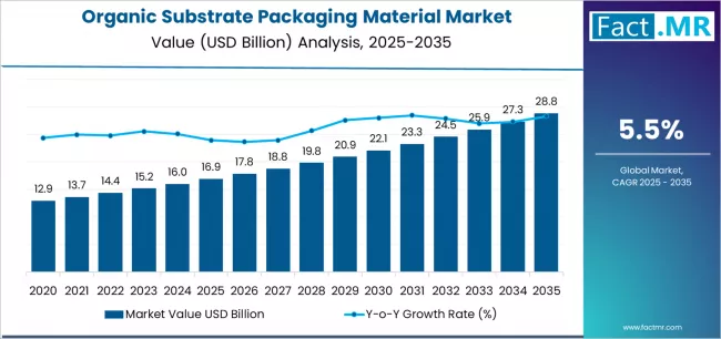
The organic substrate packaging material market is positioned for substantial expansion, driven by increasing recognition of advanced packaging importance, growing semiconductor chip complexity with enhanced performance standards, and rising adoption of sophisticated substrate technologies across electronics manufacturing practices globally.
The market demonstrates robust fundamentals supported by expanding semiconductor fabrication networks, packaging engineers' focus on thermal management protocols and rising recognition of organic substrate solutions as critical packaging components in achieving enhanced electrical performance outcomes, miniaturization capabilities, and reliability effectiveness within modern semiconductor architectures across diverse electronic applications.
Market growth is underpinned by technological innovations in substrate manufacturing procedures, particularly advanced SO package configurations and high-layer-count substrate integration, which offer enhanced signal integrity, improved thermal dissipation, and superior compatibility with comprehensive semiconductor packaging protocols prevalent in contemporary electronics practices.
Semiconductor manufacturers increasingly prioritize organic substrate materials that deliver optimal balance between electrical performance, mechanical reliability, and cost-effectiveness while adhering to increasingly stringent quality standards and miniaturization requirements across global electronics markets.
The convergence of artificial intelligence chip development in technology regions, automotive electronics growth in manufacturing economies, and specialized high-performance computing infrastructure advancement in emerging markets creates multifaceted growth opportunities for organic substrate manufacturers and semiconductor packaging operators.
The organic substrate packaging material landscape is experiencing transformative changes as manufacturers develop sophisticated substrate architectures including advanced multi-layer configurations, optimized via structures, and innovative material formulations that enable superior electrical characteristics and thermal management.
These technological advancements are complemented by evolving application capabilities encompassing AI processor packaging, advanced automotive radar systems, and innovative 5G telecommunications infrastructure that significantly improve device performance and functional integration outcomes.
The integration of heterogeneous integration technologies and advanced flip-chip capabilities further expands market opportunities for organic substrate applications, particularly benefiting high-performance computing initiatives and automotive electronics sectors where reliability optimization remains critical.
Between 2025 and 2030, the organic substrate packaging material market is projected to expand from USD 16.9 billion to USD 21.8 billion, demonstrating strong foundational growth driven by global semiconductor industry expansion, increasing awareness of advanced packaging advantages, and initial deployment of AI chip technologies across consumer electronics and automotive platforms. This growth phase establishes market infrastructure, validates high-density substrate protocols, and creates comprehensive supply networks supporting global semiconductor operations.
From 2030 to 2035, the market is forecast to reach USD 28.8 billion, driven by mature advanced packaging penetration, next-generation chiplet architectures requiring sophisticated substrate expertise, and comprehensive integration of heterogeneous integration methodologies demanding enhanced interconnect capabilities. The growing adoption of artificial intelligence accelerator programs specialized automotive ADAS initiatives, and 5G infrastructure expansion will drive demand for comprehensive organic substrate solutions with enhanced thermal profiles and seamless semiconductor packaging integration functionality.
Organic Substrate Packaging Material Market Key Takeaways
| Metric | Value |
|---|---|
| Estimated Value (2025E) | USD 16.9 billion |
| Forecast Value (2035F) | USD 28.8 billion |
| Forecast CAGR (2025 to 2035) | 5.5% |
Why is the Organic Substrate Packaging Material Market Growing?
Market expansion is being supported by the exponential increase in semiconductor content per device and the corresponding need for sophisticated packaging substrate solutions in chip integration applications across global electronics operations. Modern semiconductor professionals are increasingly focused on advanced organic substrate technologies that can enable higher I/O density, improve signal integrity, and optimize thermal management while meeting stringent reliability requirements. The proven efficacy of organic substrate materials in various semiconductor packaging applications makes them an essential component of comprehensive chip assembly strategies and advanced packaging programs.
The growing emphasis on device miniaturization standards and heterogeneous integration is driving demand for advanced organic substrate solutions that meet stringent performance specifications and operational requirements for semiconductor applications. Semiconductor manufacturers' preference for reliable, high-density substrate platforms that can ensure consistent electrical performance is creating opportunities for innovative material formulations and customized layer-stack solutions. The rising influence of artificial intelligence chip requirements and automotive electronics reliability standards is also contributing to increased adoption of premium-grade organic substrate products across different semiconductor categories and packaging systems requiring advanced interconnect technology.
Opportunity Pathways - Organic Substrate Packaging Material Market
The organic substrate packaging material market represents a transformative growth opportunity, expanding from USD 16.9 billion in 2025 to USD 28.8 billion by 2035 at a 5.5% CAGR. As semiconductor manufacturers prioritize performance optimization, thermal management enhancement, and miniaturization excellence in complex chip environments, organic substrate solutions have evolved from a basic interconnect carrier to an essential packaging component enabling precise signal routing, comprehensive thermal dissipation strategies, and multi-chip integration operations across AI processor platforms and automotive semiconductor applications.
The convergence of semiconductor complexity acceleration, increasing heterogeneous integration penetration, advanced packaging technology adoption, and stringent reliability mandates creates momentum in demand. High-performance SO package configurations offering superior I/O density, cost-effective substrate solutions balancing functionality with economics, and specialized materials for automotive applications will capture market premiums, while geographic expansion into high-growth Asian semiconductor markets and emerging OSAT ecosystems will drive volume leadership. Semiconductor manufacturer emphasis on packaging innovation and reliability provides structural support.
- Pathway A - SO Packages Technology Dominance: Leading with 41.0% market share, SO package applications drive primary demand through flip-chip ball grid array requirements requiring comprehensive high-density interconnect capabilities for advanced chip integration. Advanced SO package substrates enabling improved electrical performance, enhanced thermal management, and superior reliability outcomes command premium positioning from semiconductor manufacturers requiring stringent performance specifications and quality compliance. Expected revenue pool: USD 6.9-11.8 billion.
- Pathway B - Consumer Electronics Application Leadership: Dominating with 45.0% market share through optimal balance of volume scale and device sophistication, consumer electronics applications serve most organic substrate requirements while meeting diverse smartphone and computing demands. This application category addresses both mobile processor needs and computing chip expectations, making it the preferred segment for semiconductor companies and device manufacturers seeking comprehensive packaging capabilities. Opportunity: USD 7.6-13.0 billion.
- Pathway C - Asian Market Acceleration: India (6.6% CAGR) and China (6.4% CAGR) lead global growth through government semiconductor incentives, OSAT expansion, and substrate manufacturing capability advancement. Strategic partnerships with local foundries, technology localization expertise, and supply chain optimization enable the expansion of organic substrate applications in major semiconductor and electronics manufacturing hubs. Geographic expansion upside: USD 5.8-10.2 billion.
- Pathway D - Automotive Application Segment: Automotive electronics with growing market share serve critical safety and performance applications requiring high-reliability substrates for diverse vehicle systems. Optimized substrate configurations supporting ADAS processors, electric vehicle power management requirements, and proven automotive-grade qualification maintain significant volumes from automotive semiconductor suppliers and tier-one manufacturers. Revenue potential: USD 3.4-6.5 billion.
- Pathway E - Advanced Material Innovation & Layer-Count Expansion: Companies investing in high-layer-count substrates, novel resin formulations, and advanced via technologies gain competitive advantages through enhanced electrical performance delivery and thermal management. Advanced capabilities enabling fine-pitch interconnects and high-frequency signal integrity capture premium semiconductor partnerships. Technology premium: USD 2.5-5.2 billion.
- Pathway F - Manufacturing Excellence & Quality Assurance: Specialized substrate fabrication capabilities, strategic yield optimization, and comprehensive reliability testing systems create competitive differentiation in markets requiring consistent packaging performance. Companies offering guaranteed electrical specifications, rapid prototyping services, and comprehensive failure analysis gain preferred supplier status with quality-focused semiconductor operators. Manufacturing value: USD 2.1-4.3 billion.
- Pathway G - Emerging Applications & Market Development: Beyond traditional computing applications, organic substrates in AI accelerators, chiplet architectures, and specialized RF applications represent growth opportunities. Companies developing novel substrate architectures, supporting advanced packaging research, and expanding into adjacent semiconductor markets capture incremental demand while diversifying revenue streams. Emerging opportunity: USD 1.7-3.4 billion.
Segmental Analysis
The market is segmented by technology, application, and region. By technology, the market is divided into SO packages, GA packages, flat no-leads packages, and others. Based on application, the market is categorized into consumer electronics, automotive, manufacturing, healthcare, and others. Regionally, the market is divided into Asia Pacific, North America, Europe, Latin America, and Middle East & Africa.
Which Technology Leads in the Organic Substrate Packaging Material Market?
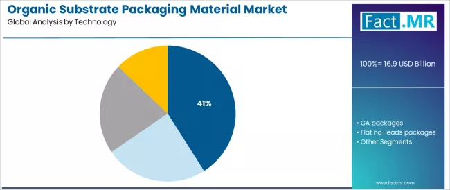
The SO packages technology segment is projected to account for 41.0% of the organic substrate packaging material market in 2025, reaffirming its position as the category's dominant packaging specification. Semiconductor packaging engineers increasingly recognize the optimal balance of I/O density and thermal performance offered by SO package substrates for flip-chip applications, particularly in high-performance computing and graphics processor packaging.
This technology category addresses both fine-pitch interconnect requirements and thermal dissipation demands while providing reliable electrical performance across diverse semiconductor operations. This segment forms the foundation of most advanced packaging protocols for high-performance chips and graphics processors, as it represents the most technically capable and commercially established technology category in the organic substrate industry.
Electrical validation standards and extensive packaging application continue to strengthen confidence in SO package substrate systems among semiconductor manufacturers and packaging professionals. With increasing recognition of interconnect density impact on chip performance and thermal management requirements, SO package substrate technologies align with both current semiconductor practices and advanced packaging evolution goals, making them the central growth driver of comprehensive chip assembly strategies across multiple application platforms.
GA packages represent a portion of technology applications, reflecting wire-bonding configurations and cost-sensitive applications requiring proven packaging approaches. Flat no-leads packages account for compact form-factor requirements, driven by mobile device miniaturization and thermal performance needs, while other technologies encompass specialized substrate configurations and emerging packaging approaches requiring distinct interconnect architectures.
Why do Consumer Electronics Command the Leading Application Share?
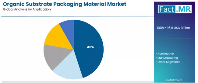
Consumer electronics application is projected to represent 45.0% of organic substrate demand in 2025, underscoring its role as the primary application category driving market adoption and substrate technology deployment. Electronics manufacturers recognize that consumer device requirements, including smartphones, tablets, and personal computers, provide the largest addressable market that specialized applications cannot match in production volume and market scale.
Organic substrates utilized in consumer electronics offer proven reliability characteristics and broad design compatibility essential for serving mass-market device requirements and cost-sensitive applications. The segment is supported by the expanding nature of global consumer electronics production, requiring packaging substrates capable of delivering adequate performance, managing thermal constraints, and providing cost-effective solutions, and the increasing recognition that organic substrate technology can enable device miniaturization.
Manufacturers are increasingly adopting advanced substrate configurations that enable compact device designs for optimal form-factor requirements and feature integration. As understanding of mobile processor capabilities advances and device performance expectations increase, consumer electronics organic substrate systems will continue to play a crucial role in comprehensive device manufacturing differentiation strategies.
Automotive applications represent growing utilization in vehicle electronics, reflecting ADAS processor packaging, electric vehicle power management, and infotainment system requirements. Manufacturing applications account for industrial automation, robotics, and production equipment requiring reliable semiconductor packaging.
Healthcare represents medical device electronics and diagnostic equipment applications, while other applications encompass specialized semiconductor packaging including telecommunications infrastructure, aerospace systems, and emerging AI accelerator markets.
What are the Drivers, Restraints, and Key Trends of the Organic Substrate Packaging Material Market?
The organic substrate packaging material market is advancing rapidly due to increasing recognition of advanced packaging importance and growing demand for high-density interconnect solutions across the semiconductor sector.
The market faces challenges, including raw material cost volatility in resin and copper foil supply, manufacturing complexity in high-layer-count substrates, and competition from alternative packaging technologies including silicon interposers. Innovation in substrate materials and advanced manufacturing methodologies continues to influence product development and market expansion patterns.
Proliferation of Artificial Intelligence Chips and High-Performance Computing
The accelerating deployment of AI processors is enabling the development of more demanding organic substrate applications and packaging protocols that can meet stringent thermal and electrical requirements.
Semiconductor designers demand comprehensive high-density substrate integration for AI chips, including massive I/O capabilities and superior thermal dissipation formulations that are particularly important for achieving adequate performance characteristics in complex AI applications.
Advanced AI chip packaging provides requirements for cutting-edge substrate technology that can optimize signal integrity strategies and manage power delivery while maintaining reliability for diverse computing environments.
Integration of Heterogeneous Integration and Chiplet Architectures
Modern semiconductor organizations are incorporating advanced technologies such as chiplet assemblies, 2.5D packaging configurations, and 3D stacking interfaces to enhance device functionality and performance scalability.
These approaches improve design flexibility, enable seamless die-to-die interconnection, and provide better integration between diverse semiconductor functions throughout the device architecture. Advanced heterogeneous integration capabilities also enable optimized power efficiency and early adoption of leading-edge process nodes or specialized functions, supporting innovative chip designs and improved performance outcomes.
Analysis of the Organic Substrate Packaging Material Market by Key Countries
| Country | CAGR (2025 to 2035) |
|---|---|
| India | 6.6% |
| China | 6.4% |
| South Korea | 6.1% |
| USA | 5.9% |
| Taiwan | 5.7% |
| Japan | 5.4% |
| Germany | 4.9% |
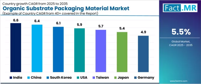
The organic substrate packaging material market is experiencing exceptional growth globally, with India leading at a 6.6% CAGR through 2035, driven by government semiconductor incentive programs, OSAT facility expansion, and comprehensive electronics manufacturing development across major industrial regions.
China follows at 6.4%, supported by massive ABF substrate manufacturing capacity, growing semiconductor self-sufficiency initiatives, and comprehensive packaging infrastructure modernization. South Korea records 6.1% growth, benefiting from advanced AI chip development and telecommunications semiconductor requirements.
USA demonstrates 5.9% growth, emphasizing high-performance computing and aerospace substrate demand. Taiwan shows 5.7% growth with TSMC advanced packaging expansion and foundry ecosystem integration. Japan records 5.4% growth, representing electronic materials innovation and precision substrate manufacturing, while Germany shows 4.9% growth, representing EV electronics and ADAS automotive substrate utilization.
How does India Demonstrate Exceptional Market Potential with Semiconductor Incentives?
The organic substrate packaging market in India is projected to exhibit exceptional growth with a CAGR of 6.6% through 2035, driven by comprehensive government semiconductor incentive programs and increasing emphasis on electronics manufacturing as an essential component for technology self-sufficiency and economic development.
The country's expanding OSAT infrastructure and growing semiconductor assembly capabilities are creating significant opportunities for organic substrate deployment across both consumer electronics and emerging automotive semiconductor segments.
Major international substrate manufacturers and domestic suppliers are establishing production relationships to serve the expanding demand from packaging facilities and electronics manufacturers requiring advanced substrate solutions across mobile devices, computing systems, and automotive electronics throughout India's diverse industrial regions.
The Indian government's strategic emphasis on semiconductor ecosystem development and electronics manufacturing promotion is driving substantial investments in packaging capabilities and substrate supply availability.
This policy support, combined with the country's enormous electronics consumption market and growing manufacturing base, creates a favorable environment for organic substrate market development. Indian OSAT facilities are increasingly focusing on advanced packaging capabilities to serve domestic and export markets, with sophisticated organic substrate systems representing a key component in this semiconductor capability building.
- Government semiconductor incentive programs and electronics manufacturing initiatives are driving demand for organic substrate solutions across packaging segments
- OSAT expansion and assembly capacity development are supporting appropriate utilization of advanced substrates among packaging facilities nationwide
- Electronics manufacturers and semiconductor companies are increasingly recognizing substrate technology importance in device performance, creating new consumption capabilities
- Rising semiconductor investment and growing awareness of advanced packaging benefits are accelerating organic substrate adoption across application categories
What Makes China Demonstrate Strong Market Growth with Manufacturing Scale?
The organic substrate packaging market in China is expanding at a CAGR of 6.4%, supported by massive ABF substrate manufacturing capacity, expanding semiconductor foundry infrastructure, and advancing packaging technology integration across the country's developing semiconductor corridors.
The country's substantial electronics production scale and increasing semiconductor self-sufficiency priorities are driving demand for domestically produced organic substrate solutions in both consumer electronics and emerging AI chip applications. International substrate suppliers and domestic manufacturers are establishing production capacity to serve the growing demand from local foundries and OSAT facilities while supporting the country's position as a leading semiconductor packaging market.
China's semiconductor sector continues to benefit from favorable government policies supporting domestic supply chain development, expanding foundry investments, and growing packaging sophistication. The country's focus on reducing foreign technology dependence is driving investments in critical substrate manufacturing including ABF production and advanced organic substrate capabilities. This development is particularly important for advanced packaging applications, as semiconductor companies seek reliable domestic substrate sources to enhance supply security and meet packaging requirements.
- Semiconductor self-sufficiency initiatives and supply chain localization are creating opportunities for domestic organic substrate solutions
- Growing foundry capacity and advanced packaging adoption are supporting increased deployment of sophisticated substrates across semiconductor categories
- Expanding ABF manufacturing capabilities and emerging material innovation are driving applications of organic substrates in computing and AI applications
- Manufacturing scale advantages are enabling cost-competitive substrate production, supporting market growth and domestic supply chain development
How does South Korea Maintain Advanced Semiconductor Leadership?
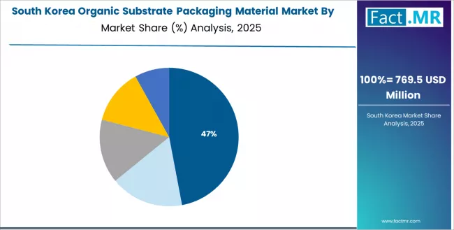
The organic substrate packaging market in South Korea is projected to exhibit strong growth with a CAGR of 6.1% through 2035, driven by advanced AI chip development and telecommunications semiconductor requirements. The country's position as a memory and logic semiconductor leader and sophisticated packaging capabilities are creating significant opportunities for organic substrate integration across both cutting-edge processor and specialized RF applications. Korean semiconductor manufacturers and substrate suppliers are leveraging technology expertise to serve the demand for high-performance substrates while supporting the country's position as a semiconductor innovation leader.
The South Korean market benefits from integrated semiconductor ecosystem supporting advanced packaging adoption, enabling optimized organic substrate utilization and comprehensive technology integration. This development is particularly important for organic substrate applications, as semiconductor companies seek performance-optimized substrates that maximize chip capabilities while ensuring reliability in advanced node and high-performance applications.
Strategic Market Considerations:
- AI processor and 5G semiconductor segments leading demand with focus on high-performance substrates and advanced packaging applications
- Integrated device manufacturer requirements and advanced node adoption are driving sophisticated organic substrate specifications with high-density characteristics
- Semiconductor technology leadership and packaging innovation supporting competitive positioning in Asian electronics markets
- Performance requirements and thermal management challenges ensuring appropriate substrate selection and material optimization
What drives USA’s Market Growth with HPC Excellence?
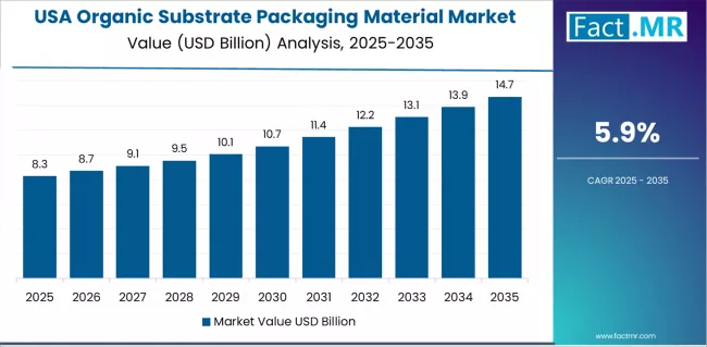
The USA's advanced semiconductor market demonstrates sophisticated organic substrate utilization with documented effectiveness in high-performance computing platforms and aerospace applications through integration with cutting-edge packaging technologies and reliability requirements.
The country leverages semiconductor design leadership and comprehensive computing infrastructure to maintain a 5.9% CAGR through 2035. Technology companies and semiconductor manufacturers, including major processor designers and fabless companies, showcase advanced organic substrate implementations where high-layer-count configurations integrate with comprehensive thermal management programs and ongoing performance optimization to maximize computing capabilities and system reliability.
American semiconductor companies prioritize performance leadership and technological innovation in chip design, creating demand for premium organic substrate solutions with proven capabilities, including ultra-fine pitch interconnects and integration with advanced heat dissipation systems. The market benefits from established semiconductor ecosystem and willingness to invest in cutting-edge packaging technologies that provide superior computational performance and compliance with aerospace reliability standards and data center requirements.
Strategic Market Considerations:
- High-performance computing and aerospace segments leading adoption with focus on advanced substrate technologies and comprehensive reliability applications
- Strong semiconductor design capabilities and packaging innovation supporting organic substrate market development through performance requirements
- Technology leadership and thermal management expertise supporting continued advancement in North American markets
- Performance standards and reliability requirements ensuring appropriate substrate specifications and quality optimization
How Does Taiwan Drive Foundry Ecosystem Integration?
The organic substrate packaging market in Taiwan is projected to exhibit moderate growth with a CAGR of 5.7% through 2035, driven by TSMC advanced packaging expansion and comprehensive foundry ecosystem development. The country's position as the leading semiconductor foundry hub and growing advanced packaging capabilities are creating opportunities for organic substrate integration across both logic processors and specialized semiconductor applications. Taiwanese foundries and substrate suppliers are leveraging manufacturing excellence to serve the demand for packaging substrates while supporting the country's position as a semiconductor manufacturing leader.
The Taiwanese market benefits from integrated foundry-packaging operations supporting substrate consumption, enabling coordinated organic substrate deployment and comprehensive supply chain integration. This development is particularly important for organic substrate applications, as foundries seek reliable substrate partners that ensure supply continuity while meeting advanced packaging requirements in leading-edge semiconductor production.
Strategic Market Considerations:
- Advanced packaging and chiplet segments leading adoption with focus on foundry integration and comprehensive substrate applications
- TSMC ecosystem development and CoWoS technology expansion are driving organic substrate consumption through advanced packaging services
- Manufacturing excellence and supply chain integration supporting competitive positioning in global semiconductor markets
- Technology roadmap alignment and capacity coordination ensuring appropriate substrate supply and packaging capability development
What Drives Japan Market Growth with Materials Innovation?
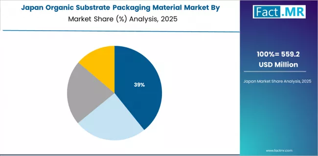
The organic substrate packaging market in Japan is projected to exhibit moderate growth with a CAGR of 5.4% through 2035, driven by electronic materials innovation and precision substrate manufacturing capabilities. The country's leadership in specialty chemicals and advanced materials development are creating opportunities for organic substrate technology advancement across both domestic semiconductor and export applications. Japanese materials companies and substrate manufacturers are leveraging technical expertise to serve the demand for high-quality substrates while supporting advanced packaging requirements.
The Japanese market benefits from materials science leadership supporting substrate innovation, enabling optimized material formulations and comprehensive quality assurance. This development is particularly important for organic substrate applications, as manufacturers develop novel resin systems and copper foil technologies that enhance substrate performance while ensuring reliability in demanding applications.
Strategic Market Considerations:
- Materials innovation and precision manufacturing segments leading development with emphasis on substrate quality and performance optimization
- Electronic materials expertise and manufacturing precision supporting organic substrate technology advancement
- Quality standards and reliability focus supported by materials industry capabilities and process control excellence
- Export markets and domestic semiconductor applications driving balanced substrate demand and technology development
How does Germany Demonstrate Automotive Electronics Leadership?
The organic substrate packaging market in Germany is projected to exhibit moderate growth with a CAGR of 4.9% through 2035, driven by electric vehicle electronics expansion and ADAS semiconductor requirements. The country's position as an automotive manufacturing leader and growing automotive semiconductor content are creating opportunities for organic substrate utilization in automotive-grade packaging applications. German automotive suppliers and semiconductor manufacturers are increasingly prioritizing reliable substrates that support vehicle electronics advancement.
The German market shows automotive-driven demand supporting specialized substrate adoption, enabling automotive-qualified organic substrates and comprehensive reliability validation. This development is particularly relevant for organic substrate applications, as automotive manufacturers require stringent quality standards and long-term reliability assurance in safety-critical electronic systems.
Strategic Market Considerations:
- Automotive electronics and industrial segments representing growth focus with emphasis on reliability and automotive-grade qualification
- Electric vehicle electronics and ADAS semiconductor requirements driving demand for high-reliability organic substrates
- Automotive quality standards and AEC-Q qualification influencing substrate specifications and supplier selection
- Long-term reliability requirements and environmental durability ensuring appropriate material selection and testing validation
Europe Market Split by Country
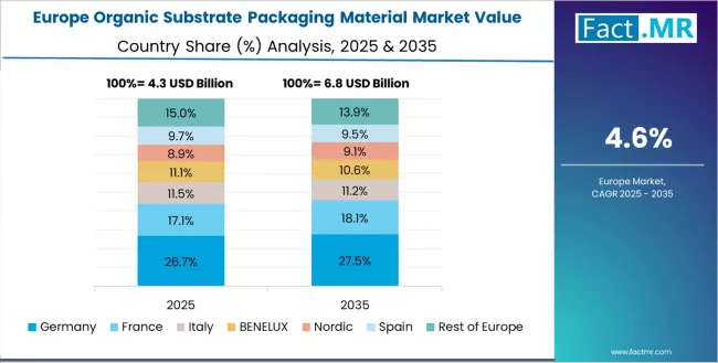
The organic substrate packaging material market in Europe is projected to grow from USD 3.2 billion in 2025 to USD 5.1 billion by 2035, registering a CAGR of 4.8% over the forecast period. Germany is expected to maintain its leadership position with a 34.6% market share in 2025, rising to 36.2% by 2035, supported by its dominant automotive electronics infrastructure, comprehensive manufacturing capabilities, and advanced substrate quality excellence throughout major semiconductor assembly facilities and automotive supply networks.
France follows with a 22.4% share in 2025, projected to reach 21.8% by 2035, driven by industrial electronics sophistication, aerospace semiconductor applications, and established substrate distribution serving both domestic and European markets. The UK holds a 16.8% share in 2025, expected to decrease to 15.4% by 2035, reflecting mature market characteristics and limited local substrate manufacturing.
Italy commands a 13.7% share in 2025, projected to reach 13.2% by 2035, while the Netherlands accounts for 9.3% in 2025, expected to reach 9.8% by 2035. The rest of Europe region, including Nordic countries with specialty electronics, Eastern European emerging assembly markets, and smaller Western European semiconductor facilities, is anticipated to hold 3.2% in 2025, increasing slightly to 3.6% by 2035, attributed to regional electronics manufacturing growth in select markets with developing packaging infrastructure and organic substrate consumption.
Competitive Landscape of the Organic Substrate Packaging Material Market
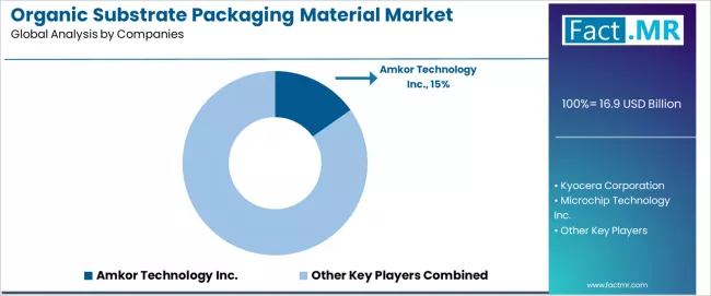
The organic substrate packaging material market is characterized by intense competition among established substrate manufacturers, specialized OSAT providers, and comprehensive semiconductor packaging organizations focused on delivering high-quality, reliable, and performance-optimized organic substrate products.
Companies are investing in manufacturing capacity expansion programs, advanced material development, strategic foundry partnerships, and comprehensive quality assurance initiatives to deliver effective, consistent, and technologically advanced substrate solutions that meet stringent semiconductor standards and customer expectations. Product innovation, yield optimization, and technical support strategies are central to strengthening product portfolios and market presence.
Amkor Technology Inc. leads the market with a 15.2% market share, offering comprehensive semiconductor packaging solutions with integrated organic substrate capabilities focusing on OSAT expertise and advanced flip-chip packaging for diverse semiconductor applications. Kyocera Corporation provides specialized ceramic and organic substrate platforms with emphasis on material science excellence and comprehensive electronic component support across global markets.
Microchip Technology Inc. focuses on integrated semiconductor solutions and substrate requirements serving microcontroller and analog applications. Texas Instruments Incorporated delivers semiconductor manufacturing expertise with captive substrate capabilities and power management integration.
ASE Kaohsiung operates with a focus on advanced packaging services and organic substrate consumption for semiconductor assembly applications. Simmtech Co., Ltd provides Korean substrate manufacturing emphasizing mobile device applications and consumer electronics integration.
Shinko Electric Industries Co. Ltd specializes in Japanese substrate production and high-density interconnect expertise. LG Innotek Co. Ltd delivers substrate manufacturing to enhance consumer electronics supply and provide comprehensive packaging solutions. AT&S and Daeduck Electronics Co. Ltd focus on European and Korean substrate production capabilities, emphasizing manufacturing quality and comprehensive substrate protocols through dedicated organic packaging strategies.
Key Players in the Organic Substrate Packaging Material Market
- Amkor Technology Inc.
- Kyocera Corporation
- Microchip Technology Inc.
- Texas Instruments Incorporated
- ASE Kaohsiung
- Simmtech Co., Ltd
- Shinko Electric Industries Co. Ltd
- LG Innotek Co. Ltd
- AT&S
- Daeduck Electronics Co. Ltd
Scope of the Report
| Items | Values |
|---|---|
| Quantitative Units (2025) | USD 16.9 Billion |
| Technology | SO packages, GA packages, Flat no-leads packages, Others |
| Application | Consumer Electronics, Automotive, Manufacturing, Healthcare, Others |
| Regions Covered | Asia Pacific, North America, Europe, Latin America, Middle East & Africa |
| Countries Covered | USA, Germany, UK, Japan, India, China, South Korea, Taiwan and 40+ countries |
| Key Companies Profiled | Amkor Technology Inc., Kyocera Corporation, Microchip Technology Inc., Texas Instruments Incorporated, ASE Kaohsiung, Simmtech Co., Ltd, Shinko Electric Industries Co. Ltd, LG Innotek Co. Ltd, AT&S, Daeduck Electronics Co. Ltd |
| Additional Attributes | Dollar sales by technology, application, regional demand trends, competitive landscape, semiconductor manufacturer preferences for specific organic substrate configurations, integration with comprehensive packaging systems, innovations in substrate material development, layer-count advancement, and electrical performance optimization capabilities |
Organic Substrate Packaging Material Market by Segments
-
Technology :
- SO packages
- GA packages
- Flat no-leads packages
- Others
-
Application :
- Consumer Electronics
- Automotive
- Manufacturing
- Healthcare
- Others
-
Region :
- Asia Pacific
- China
- India
- Japan
- South Korea
- Taiwan
- ASEAN
- Australia & New Zealand
- Rest of Asia Pacific
- North America
- United States
- Canada
- Mexico
- Europe
- Germany
- France
- United Kingdom
- Italy
- Spain
- Nordic
- BENELUX
- Rest of Europe
- Latin America
- Brazil
- Argentina
- Chile
- Rest of Latin America
- Middle East & Africa
- Kingdom of Saudi Arabia
- Other GCC Countries
- Turkey
- South Africa
- Other African Countries
- Rest of Middle East & Africa
- Asia Pacific
- Frequently Asked Questions -
How big is the organic substrate packaging material market in 2025?
The global organic substrate packaging material market is estimated to be valued at USD 16.9 billion in 2025.
What will be the size of organic substrate packaging material market in 2035?
The market size for the organic substrate packaging material market is projected to reach USD 28.8 billion by 2035.
How much will be the organic substrate packaging material market growth between 2025 and 2035?
The organic substrate packaging material market is expected to grow at a 5.5% CAGR between 2025 and 2035.
What are the key product types in the organic substrate packaging material market?
The key product types in organic substrate packaging material market are so packages, ga packages, flat no-leads packages and others.
Which application segment to contribute significant share in the organic substrate packaging material market in 2025?
In terms of application, consumer electronics segment to command 45.0% share in the organic substrate packaging material market in 2025.
Table of Content
- Executive Summary
- USA Market Outlook
- Demand to side Trends
- Supply to side Trends
- Technology Roadmap Analysis
- Analysis and Recommendations
- Market Overview
- Market Coverage / Taxonomy
- Market Definition / Scope / Limitations
- Market Background
- Market Dynamics
- Drivers
- Restraints
- Opportunity
- Trends
- Scenario Forecast
- Demand in Optimistic Scenario
- Demand in Likely Scenario
- Demand in Conservative Scenario
- Opportunity Map Analysis
- Product Life Cycle Analysis
- Supply Chain Analysis
- Investment Feasibility Matrix
- Value Chain Analysis
- PESTLE and Porter’s Analysis
- Regulatory Landscape
- Regional Parent Market Outlook
- Production and Consumption Statistics
- Import and Export Statistics
- Market Dynamics
- USA Market Analysis 2020 to 2024 and Forecast, 2025 to 2035
- Historical Market Size Value (USD Million) Analysis, 2020 to 2024
- Current and Future Market Size Value (USD Million) Projections, 2025 to 2035
- Y to o to Y Growth Trend Analysis
- Absolute $ Opportunity Analysis
- USA Market Pricing Analysis 2020 to 2024 and Forecast 2025 to 2035
- USA Market Analysis 2020 to 2024 and Forecast 2025 to 2035, By Technology
- Introduction / Key Findings
- Historical Market Size Value (USD Million) Analysis By Technology, 2020 to 2024
- Current and Future Market Size Value (USD Million) Analysis and Forecast By Technology, 2025 to 2035
- SO packages
- GA packages
- Flat no-leads packages
- Others
- Y to o to Y Growth Trend Analysis By Technology, 2020 to 2024
- Absolute $ Opportunity Analysis By Technology, 2025 to 2035
- USA Market Analysis 2020 to 2024 and Forecast 2025 to 2035, By Application
- Introduction / Key Findings
- Historical Market Size Value (USD Million) Analysis By Application, 2020 to 2024
- Current and Future Market Size Value (USD Million) Analysis and Forecast By Application, 2025 to 2035
- Consumer Electronics
- Automotive
- Manufacturing
- Healthcare
- Others
- Y to o to Y Growth Trend Analysis By Application, 2020 to 2024
- Absolute $ Opportunity Analysis By Application, 2025 to 2035
- USA Market Analysis 2020 to 2024 and Forecast 2025 to 2035, By Region
- Introduction
- Historical Market Size Value (USD Million) Analysis By Region, 2020 to 2024
- Current Market Size Value (USD Million) Analysis and Forecast By Region, 2025 to 2035
- USA
- Market Attractiveness Analysis By Region
- USA Market Analysis 2020 to 2024 and Forecast 2025 to 2035, By Country
- Historical Market Size Value (USD Million) Trend Analysis By Market Taxonomy, 2020 to 2024
- Market Size Value (USD Million) Forecast By Market Taxonomy, 2025 to 2035
- By Country
- By Technology
- By Application
- Market Attractiveness Analysis
- By Country
- By Technology
- By Application
- Key Takeaways
- Market Structure Analysis
- Competition Dashboard
- Competition Benchmarking
- Market Share Analysis of Top Players
- By Regional
- By Technology
- By Application
- Competition Analysis
- Competition Deep Dive
- Amkor Technology Inc.
- Overview
- Product Portfolio
- Profitability by Market Segments (Product/Age /Sales Channel/Region)
- Sales Footprint
- Strategy Overview
- Marketing Strategy
- Product Strategy
- Channel Strategy
- Kyocera Corporation
- Microchip Technology Inc.
- Texas Instruments Incorporated
- ASE Kaohsiung
- Simmtech Co., Ltd
- Shinko Electric Industries Co. Ltd
- LG Innotek Co. Ltd
- AT&S
- Daeduck Electronics Co. Ltd
- Amkor Technology Inc.
- Competition Deep Dive
- Assumptions & Acronyms Used
- Research Methodology
List Of Table
- Table 1: USA Market Value (USD Million) Forecast by Region, 2020 to 2035
- Table 2: USA Market Value (USD Million) Forecast by Technology, 2020 to 2035
- Table 3: USA Market Value (USD Million) Forecast by Application, 2020 to 2035
- Table 4: USA Market Value (USD Million) Forecast by Country, 2020 to 2035
- Table 5: USA Market Value (USD Million) Forecast by Technology, 2020 to 2035
- Table 6: USA Market Value (USD Million) Forecast by Application, 2020 to 2035
List Of Figures
- Figure 1: USA Market Pricing Analysis
- Figure 2: USA Market Value (USD Million) Forecast 2020 to 2035
- Figure 3: USA Market Value Share and BPS Analysis by Technology, 2025 and 2035
- Figure 4: USA Market Y to o to Y Growth Comparison by Technology, 2025 to 2035
- Figure 5: USA Market Attractiveness Analysis by Technology
- Figure 6: USA Market Value Share and BPS Analysis by Application, 2025 and 2035
- Figure 7: USA Market Y to o to Y Growth Comparison by Application, 2025 to 2035
- Figure 8: USA Market Attractiveness Analysis by Application
- Figure 9: USA Market Value (USD Million) Share and BPS Analysis by Region, 2025 and 2035
- Figure 10: USA Market Y to o to Y Growth Comparison by Region, 2025 to 2035
- Figure 11: USA Market Attractiveness Analysis by Region
- Figure 12: USA Market Incremental Dollar Opportunity, 2025 to 2035
- Figure 13: USA Market Value Share and BPS Analysis by Country, 2025 and 2035
- Figure 14: USA Market Value Share and BPS Analysis by Technology, 2025 and 2035
- Figure 15: USA Market Y to o to Y Growth Comparison by Technology, 2025 to 2035
- Figure 16: USA Market Attractiveness Analysis by Technology
- Figure 17: USA Market Value Share and BPS Analysis by Application, 2025 and 2035
- Figure 18: USA Market Y to o to Y Growth Comparison by Application, 2025 to 2035
- Figure 19: USA Market Attractiveness Analysis by Application
- Figure 20: USA Market - Tier Structure Analysis
- Figure 21: USA Market - Company Share Analysis