- Market Value (2025): USD 614.5 Mn
- Estimated Value (2026): USD 695.0 Mn
- Forecast Value (2036): USD 2380.0 Mn
- CAGR (2026-2036): 13.1%
What is the Sub-Nanometer eBeam Market forecast to be worth by 2036?
USD 695.0 million in 2026 to USD 2,380.0 million by 2036, at a 13.1% CAGR.
- The Sub-Nanometer eBeam Market crossed a valuation of USD 614.5 million in 2025. Foundries use e-beam inspection and metrology to review defects, measure critical dimensions and feed process-control decisions at advanced nodes.
- Demand is projected to increase from USD 695.0 million in 2026 to USD 2,380.0 million by 2036.
- The market is forecast to record a 13.1% CAGR from 2026 to 2036.
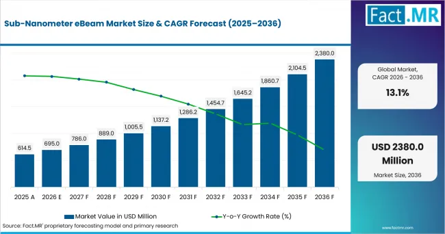
Sub Nanometer EBeam Market Value Analysis | Source: Fact.MR
What are the defining numbers behind Sub-Nanometer eBeam Market growth?
USD 1,685.0 million absolute opportunity is expected by 2036.
- Demand Drivers in the Market
- Inspection sensitivity and throughput: Advanced-node fabs need to find yield-limiting defects at dimensions where optical inspection alone may not provide sufficient sensitivity, while still preserving usable wafer coverage. E-beam selection therefore depends on defect size, sampling coverage and cycle-time limits. [1][2]
- Single-beam inspection: KLA's eSL10 uses a single high-current-density beam. Its Yellowstone mode processes 10 billion pixels per scan, while Simul-6 collects surface, topographic, material-contrast and deep-trench information in one scan. These capabilities support demand where fabs need high-sensitivity defect review across varied process layers without separate scans for each signal type. [1]
- Multibeam inspection: ASML's HMI eScan 1100 uses 25 beams and a high-speed wafer stage to increase inspection throughput. Its physical-defect and voltage-contrast capability makes it relevant where leading-edge fabs need more wafer coverage for electrical and patterning-defect inspection. [2]
- Voltage-contrast inspection: E-beam systems can detect electrical defects including opens, shorts and leakage defects. Demand arises where advanced logic and memory layers require reliable electrical-defect detection beyond optical coverage; charging control and landing-energy selection shape tool qualification. [2]
- Key Segments Analyzed
- By System Type: CD-SEM systems are projected to hold 32.0% share in 2026: CD-SEM systems convert electron imaging into repeatable dimensional measurements with established calibration, recipe and statistical-control workflows. They are sampled frequently across process steps and therefore create the largest sustained sub-nanometer measurement workload.
- By Resolution Class: <0.5 nm is projected to hold 38.8% share in 2026: Resolution below 0.5 nanometers provides additional measurement margin for demanding critical-dimension, edge-placement and roughness measurements. Adoption depends on the process layer, signal quality, charging behavior, sampling coverage and repeatability requirements.
- By Beam Architecture: Single-beam columns are projected to hold 42.4% share in 2026: Single-beam columns concentrate current and detector optimization on one probe, supporting high-sensitivity CD measurement and defect review. Multibeam architectures provide greater parallel coverage but require calibration and data processing across multiple beams.
- By Application: Critical dimension metrology is projected to hold 41.3% share in 2026: Critical-dimension metrology requires calibrated, repeatable measurements at many process checkpoints and directly feeds process control. The recurring sampling cadence creates a larger installed workload than occasional high-resolution defect analysis.
- By End User: Foundries are projected to hold 29.3% share in 2026: Foundries support many customer layouts at leading nodes and need dense metrology feedback to keep shared process modules centered. A sub-nanometer measurement error can affect multiple products simultaneously.
- Analyst Opinion at Fact.MR
- Shambhu Nath Jha, Sr. Consultant at Fact.MR, states, 'For advanced-node fabs, the purchase case is not resolution alone. A system must find yield-limiting defects in target layers at a sampling rate that supports process control, while managing charging and correlating results with optical inspection.'
- Strategic Implications
- Fabs should evaluate defects of interest per hour, charging control, voltage-contrast capability and correlation to optical inspection.
- Equipment suppliers should document measurement repeatability, charging control, signal collection, scan strategy and correlation with established inspection workflows on production-representative wafers.
- Procurement teams should compare defects of interest per hour, usable sampling coverage, charging behavior, recipe stability and service response before selecting a platform.
USA is projected to record a 14.7% CAGR; Taiwan, 14.5%; South Korea, 14.0%; Japan, 13.5%; and the Netherlands, 12.9% from 2026 to 2036. Demand conditions differ by country: leading-edge logic and semiconductor R&D shape the USA outlook, foundry and packaging capacity matter in Taiwan, memory and HBM production support South Korea, equipment and metrology expertise support Japan, and semiconductor-equipment R&D supports the Netherlands.
How does the Sub-Nanometer eBeam Market break down by segment?
CD-SEM systems lead System Type with a 32.0% share, while <0.5 nm accounts for 38.8% of Resolution Class in 2026.
Why do CD-SEM systems lead System Type?
CD-SEM systems are projected to account for 32.0% share in 2026.
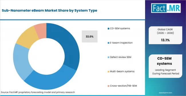
Sub Nanometer EBeam Market Analysis By System Type | Source: Fact.MR
Why does <0.5 nm lead Resolution Class?
<0.5 nm is projected to account for 38.8% share in 2026.
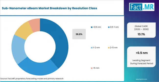
Sub Nanometer EBeam Market Analysis By Resolution Class | Source: Fact.MR
Resolution below 0.5 nanometers can provide additional measurement margin when critical dimensions, edge placement and roughness require tighter control. The 0.5-1 nanometer class remains suitable where the measurement target and process tolerance do not require the highest available resolution. Tool selection depends on charging behavior, signal quality, sampling coverage and measurement repeatability.
Why do Single-beam columns lead Beam Architecture?
Single-beam columns are projected to account for 42.4% share in 2026.
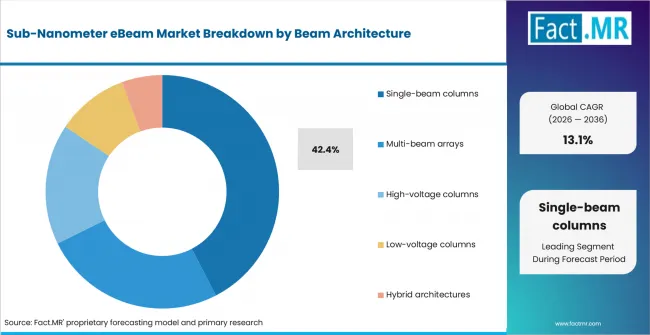
Sub Nanometer EBeam Market Analysis By Beam Architecture | Source: Fact.MR
Single-beam columns concentrate current and detector optimization on one probe, supporting high-sensitivity CD measurement and defect review. Multibeam arrays trade a more complex calibration and data-processing task for greater parallel coverage. KLA's eSL10 uses a single high-current-density beam with Yellowstone scanning and Simul-6 detection, while ASML's eScan 1100 uses 25 beams to increase inspection throughput. [1][2]
Why does Critical dimension metrology lead Application?
Critical dimension metrology is projected to account for 41.3% share in 2026.
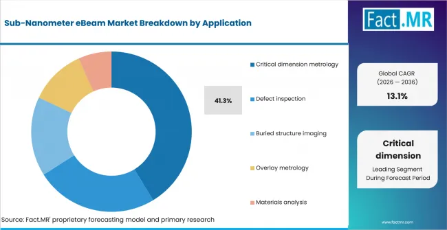
Sub Nanometer EBeam Market Analysis By Application | Source: Fact.MR
Critical-dimension metrology requires calibrated, repeatable measurements at multiple process checkpoints and feeds process control directly. Defect inspection covers broader areas but is often targeted to hotspots or engineering wafers because scan time limits coverage. Voltage-contrast inspection can detect electrical defects including opens, shorts and leakage defects on advanced logic and memory layers. [2]
Why do Foundries lead End User?
Foundries are projected to account for 29.3% share in 2026.
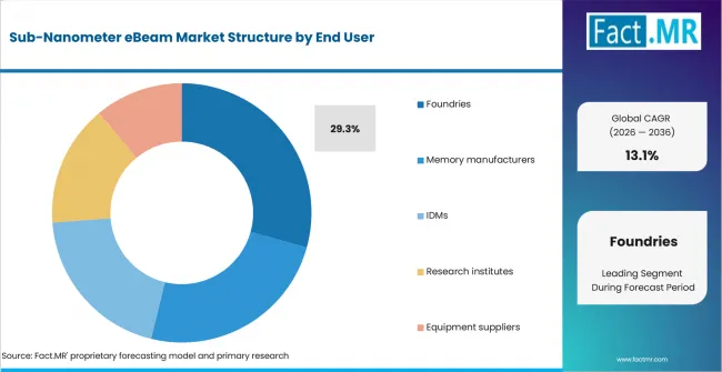
Sub Nanometer EBeam Market Analysis By End User | Source: Fact.MR
Foundries support many customer layouts at leading nodes and need dense metrology feedback to keep shared process modules centered. A sub-nanometer measurement error can affect multiple products. KLA documents Yellowstone scanning, Simul-6 signal collection and deep-learning defect isolation on its eSL10 platform; these capabilities support defect discovery across advanced logic and memory structures. [1]
What is accelerating Sub-Nanometer eBeam Market adoption, and what is holding it back?
The strongest accelerator is the need to inspect smaller defects without losing usable wafer coverage. The main restraint is the trade-off among scan time, data volume, charging control and sensitivity.
The following factors shape demand but are not assigned a separate contribution to the forecast CAGR.
Drivers Impact Analysis
| DRIVER | MARKET RELEVANCE | PRIMARY ADOPTION CONTEXT | RELEVANCE HORIZON |
|---|---|---|---|
| Inspection sensitivity and throughput | High | Global leading-edge fabs | 2026 to 2036 |
| Flagship single-beam capability | High | Global leading-edge fabs | 2026 to 2036 |
| Multibeam for throughput | High | Global leading-edge fabs | 2026 to 2036 |
| Voltage-contrast inspection | High | Global leading-edge fabs | 2026 to 2036 |
Source: Fact.MR analysis. Updated Jul 23, 2026
- Inspection sensitivity and throughput: Optical inspection supports broad coverage, while e-beam systems provide higher-resolution review for selected defects and process layers. Fabs balance sampling coverage, scan time and charging behavior when assigning inspection steps. [1][2]
- Flagship single-beam capability: KLA's eSL10 uses a single high-current-density beam, Yellowstone scanning to produce 10 billion pixels per scan, Simul-6 signal collection and deep-learning defect isolation. [1]
- Multibeam for throughput: ASML's HMI eScan 1100 uses 25 beams and provides up to 15 times the throughput of single e-beam inspection tools. It supports voltage-contrast inspection and wafer-print checks for EUV mask defects. [2]
- Voltage-contrast inspection: Voltage contrast identifies electrical defects such as opens, shorts and leakage defects in advanced logic and memory structures. [2]
Opportunity Impact Analysis
| OPPORTUNITY | MARKET RELEVANCE | PRIMARY ADOPTION CONTEXT | RELEVANCE HORIZON |
|---|---|---|---|
| Single-beam smarter scanning vs multibeam parallelism | Moderate | Global leading-edge fabs | 2026 to 2036 |
| Deep-learning defect classification | Moderate | Global leading-edge fabs | 2026 to 2036 |
| EUV inspection requirements | Moderate | Global leading-edge fabs | 2026 to 2036 |
Source: Fact.MR analysis. Updated Jul 23, 2026
- Single-beam smarter scanning vs multibeam parallelism: Single-beam systems concentrate current and detector performance on one probe, while multibeam systems increase parallel coverage. The opportunity lies in matching architecture to defect sensitivity, sampling area and acceptable scan time.
- Deep-learning defect classification: KLA integrates deep-learning algorithms to isolate defects most critical to device performance. [1]
- EUV inspection requirements: Smaller features and EUV mask monitoring create additional inspection and metrology work in mask shops and wafer fabs. ASML documents wafer-print checks for EUV mask-defect monitoring on the eScan 1100. [2]
Restraints Impact Analysis
| RESTRAINT | MARKET RELEVANCE | PRIMARY ADOPTION CONTEXT | RELEVANCE HORIZON |
|---|---|---|---|
| Primary qualification constraint | High | Global leading-edge fabs | 2026 to 2036 |
| Throughput versus sensitivity | High | Global leading-edge fabs | 2026 to 2036 |
| Process-window sensitivity | Moderate | Global leading-edge fabs | 2026 to 2036 |
Source: Fact.MR analysis. Updated Jul 23, 2026
- Primary qualification constraint: Scan time, data volume and sample charging limit the wafer area that can be inspected at the required sensitivity.
- Throughput versus sensitivity: Higher-resolution review generally reduces coverage unless scan strategy, stage speed or parallel beams recover throughput.
- Process-window sensitivity: Landing energy, charging control, detector configuration and classification thresholds must be qualified for each layer and defect type.
Which countries are scaling Sub-Nanometer eBeam Market fastest?
In USA, the Sub-Nanometer eBeam Market is projected to advance at a 14.7% CAGR from 2026 to 2036.
- Countries differ less by the headline CAGR than by the type of semiconductor work creating demand for the Sub-Nanometer eBeam Market.
- USA follows a pathway shaped by leading-edge logic, high-performance computing, federally supported semiconductor R&D and a large domestic equipment base. Taiwan takes a different path through leading foundry production, advanced packaging and a dense OSAT and substrate supply chain.
- South Korea remains differentiated by its concentration of high-volume memory and HBM manufacturing.
- Japan develops through semiconductor equipment, materials and metrology expertise, while the Netherlands is linked to lithography-integrated inspection and computational metrology.
- Sub-nanometer eBeam demand depends on advanced-node inspection insertion, foundry and memory capacity, optical-to-eBeam correlation, equipment access and qualification cycles, even where country CAGRs are close.
Country analysis situates the five profiled markets within North America, Latin America, Europe, East Asia, South Asia & Oceania, and the Middle East & Africa.
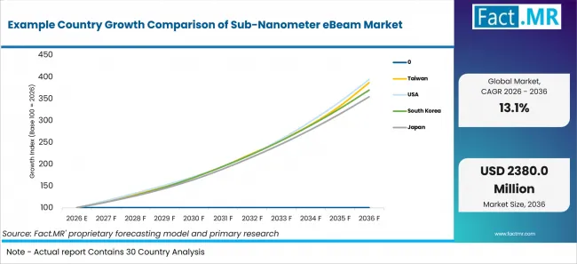
Example Country Growth Comparison Of Sub Nanometer EBeam Market | Source: Fact.MR
| COUNTRY | CAGR, 2026 to 2036 |
|---|---|
| USA | 14.7% |
| Taiwan | 14.5% |
| South Korea | 14.0% |
| Japan | 13.5% |
| Netherlands | 12.9% |
Source: Fact.MR analysis. Updated Jul 23, 2026
What is driving USA's growth through 2036?
The USA market is projected to grow at a 14.7% CAGR from 2026 to 2036.
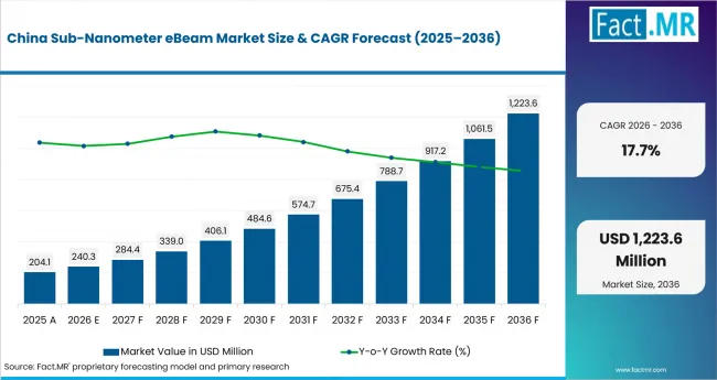
Sub Nanometer EBeam Market Country Value Analysis | Source: Fact.MR
The USA outlook reflects leading-edge logic, high-performance computing and semiconductor R&D activity. KLA's eSL10 is cited as an example of inspection capability used in this environment, not as the basis for the country forecast. [1]
What is driving Taiwan's growth through 2036?
The Taiwan market is projected to grow at a 14.5% CAGR from 2026 to 2036.
The Taiwan outlook reflects leading foundry production, advanced packaging and a dense semiconductor supply chain. ASML's HMI eScan 1100 is cited as an example of inspection capability relevant to this environment, not as the basis for the country forecast. [2]
What is driving South Korea's growth through 2036?
The South Korea market is projected to grow at a 14.0% CAGR from 2026 to 2036.
The South Korea outlook reflects high-volume memory and HBM manufacturing, where buried defects, voltage contrast and process-window control shape inspection requirements. The country forecast remains an aggregate projection rather than a result of any one device category or tool qualification.
What is driving Japan's growth through 2036?
The Japan market is projected to grow at a 13.5% CAGR from 2026 to 2036.
Japan's outlook reflects its semiconductor equipment, materials and metrology base. Hitachi High-Tech's GS1000 is cited as evidence of local inspection capability, not as the basis for the country forecast. [4]
What is driving the Netherlands' growth through 2036?
The Netherlands market is projected to grow at a 12.9% CAGR from 2026 to 2036.
The Netherlands outlook reflects its semiconductor-equipment base and EUV-related inspection expertise. ASML's HMI eScan 1100 is cited as an example of available capability, not as the basis for the country forecast. [2]
Which companies are the key providers?
Key companies include Applied Materials; Hitachi High-Tech; KLA; ASML (HMI); Zeiss; JEOL.
- Applied Materials
- Hitachi High-Tech
- KLA
- ASML (HMI)
- Zeiss
- JEOL
Bibliography
- [1] KLA. (2020, July 20). KLA Introduces Breakthrough Electron-Beam Defect Inspection System.
- [2] ASML. HMI eScan 1100.
- [3] Applied Materials. PROVision 10 eBeam Metrology.
- [4] Hitachi High-Tech. (2021, December 13). Hitachi High-Tech Develops the Electron Beam Area Inspection System GS1000.
- [5] ZEISS. MultiSEM Multi-Beam Electron Microscope.
- [6] JEOL. Semiconductor Inspection and Analysis Solutions.
This Report Addresses
- The report examines sub-nanometer e-beam inspection, review and metrology across the System Type and Resolution Class segments.
- CD-SEM systems lead System Type in the 2026 market structure, while the detailed analysis compares single-beam and multibeam architectures.
- Regional analysis compares the USA, Taiwan, South Korea, Japan and the Netherlands.
- Competitive analysis covers Applied Materials [3], Hitachi High-Tech [4], KLA [1], ASML (HMI) [2], ZEISS [5] and JEOL [6].
- Use-case analysis focuses on critical-dimension metrology, defect inspection, buried-structure imaging, overlay metrology and materials analysis.
What does the Sub-Nanometer eBeam Market cover?
The market covers equipment and process systems configured to address the challenge of finding nanometer-scale defects and measuring critical dimensions at useful wafer throughput.
Sub-nanometer eBeam covers electron-beam inspection, review and metrology systems used for single-nanometer and sub-nanometer measurement tasks. The category includes single-beam inspectors, multibeam wafer inspectors, CD-SEM platforms and e-beam defect-review systems. It is distinguished by high-resolution imaging, voltage-contrast capability, measurement repeatability and the need to balance sensitivity with wafer coverage.
Market value includes configured inspection or metrology platforms, wafer handling, electron optics, detectors, charging-control functions, analysis software and service elements supplied with the system. Finished devices, processed wafers and unrelated semiconductor equipment are excluded.
What is included in the scope?
The scope includes systems used by foundries and the other end-user groups listed in the segmentation.
The market is segmented by System Type, including CD-SEM systems, E-beam inspection, Defect review SEM, Multi-beam systems, Cross-section/FIB-SEM; Resolution Class, including <0.5 nm, 0.5-1 nm, 1-2 nm, 2-5 nm, >5 nm; Beam Architecture, including Single-beam columns, Multi-beam arrays, High-voltage columns, Low-voltage columns, Hybrid architectures; Application, including Critical dimension metrology, Defect inspection, Buried structure imaging, Overlay metrology, Materials analysis; End User, including Foundries, Memory manufacturers, IDMs, Research institutes, Equipment suppliers.
Wafer handling, charging control, detector modules, classification software and process-control interfaces are included when supplied as part of the configured e-beam system.
What is excluded from the scope?
The scope excludes unrelated semiconductor equipment, standalone materials and components sold independently of the configured system.
It also excludes facility construction, cleanroom infrastructure, the value of processed wafers or packages, and adjacent process steps that are not part of the defined equipment category.
How Was the Analysis Built?
Fact.MR is of the opinion that this assessment combines structured market analysis with a review of public information and industry evidence relevant to the market.
- Market Assessment: The analysis considers demand patterns, supply conditions, segment mix, country activity, company participation, and adoption trends.
- Evidence Review: Public company disclosures, government and regulatory publications, trade information, technical literature, and industry records inform the assessment.
- Validation and Updates: Findings are cross-checked against available market indicators and reviewed when material market developments emerge.
Segmentation
What is the report's scope and coverage?
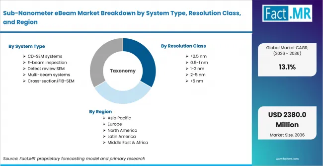
Sub Nanometer EBeam Market Breakdown By System Type, Resolution Class, And Region | Source: Fact.MR
| Attribute | Details |
|---|---|
| Quantitative Units | USD 695.0 million in 2026 to USD 2,380.0 million by 2036 at a 13.1% CAGR |
| Market Definition | Sub-nanometer eBeam covers electron-beam inspection, review and metrology systems used for single-nanometer and sub-nanometer measurement tasks. The category includes single-beam inspectors, multibeam wafer inspectors, CD-SEM platforms and e-beam defect-review systems. It is distinguished by high-resolution imaging, voltage-contrast capability, measurement repeatability and the need to balance sensitivity with wafer coverage. |
| System Type | CD-SEM systems; E-beam inspection; Defect review SEM; Multi-beam systems; Cross-section/FIB-SEM |
| Resolution Class | <0.5 nm; 0.5-1 nm; 1-2 nm; 2-5 nm; >5 nm |
| Beam Architecture | Single-beam columns; Multi-beam arrays; High-voltage columns; Low-voltage columns; Hybrid architectures |
| Application | Critical dimension metrology; Defect inspection; Buried structure imaging; Overlay metrology; Materials analysis |
| End User | Foundries; Memory manufacturers; IDMs; Research institutes; Equipment suppliers |
| Regions Covered | North America; Latin America; Europe; East Asia; South Asia & Oceania; Middle East & Africa |
| Countries Covered | Taiwan; USA; South Korea; Japan; Netherlands |
| Key Companies Profiled | Applied Materials; Hitachi High-Tech; KLA; ASML (HMI); Zeiss; JEOL |
| Forecast Period | 2026 to 2036 |
| Approach | Hybrid top-down and bottom-up approach using demand indicators across System Type; Resolution Class; Beam Architecture; Application; End User; country-level growth; company participation and adoption trends |
Source: Fact.MR analysis. Updated Jul 23, 2026
How is the market segmented?
-
By System Type:
- CD-SEM systems
- E-beam inspection
- Defect review SEM
- Multi-beam systems
- Cross-section/FIB-SEM
-
By Resolution Class:
- <0.5 nm
- 0.5-1 nm
- 1-2 nm
- 2-5 nm
- >5 nm
-
By Beam Architecture
- Single-beam columns
- Multi-beam arrays
- High-voltage columns
- Low-voltage columns
- Hybrid architectures
-
By Application:
- Critical dimension metrology
- Defect inspection
- Buried structure imaging
- Overlay metrology
- Materials analysis
-
By End User:
- Foundries
- Memory manufacturers
- IDMs
- Research institutes
- Equipment suppliers
-
By Region:
- North America
- Latin America
- Europe
- South Asia & Oceania
- Middle East & Africa
Frequently Asked Questions
Which System Type leads the Sub-Nanometer eBeam Market?
Which Resolution Class leads the Sub-Nanometer eBeam Market?
Which Beam Architecture leads the Sub-Nanometer eBeam Market?
Which Application leads the Sub-Nanometer eBeam Market?
Which End User leads the Sub-Nanometer eBeam Market?
What CAGR is projected for USA in the Sub-Nanometer eBeam Market?
What CAGR is projected for Taiwan in the Sub-Nanometer eBeam Market?
What CAGR is projected for South Korea in the Sub-Nanometer eBeam Market?
What CAGR is projected for Japan in the Sub-Nanometer eBeam Market?
What CAGR is projected for the Netherlands in the Sub-Nanometer eBeam Market?
What is the primary driver of the Sub-Nanometer eBeam Market?
What is the main restraint in the Sub-Nanometer eBeam Market?
Who worked on this report


Preview the report firsthand - request a free sample
Free SampleGet the brochure for pricing and purchase details
Download PDF