- Market Value (2025): USD 548.6 Mn
- Estimated Value (2026): USD 598.0 Mn
- Forecast Value (2036): USD 1420.0 Mn
- CAGR (2026-2036): 9.0%
What is the 3D Device eBeam Market forecast to be worth by 2036?
USD 598.0 million in 2026 to USD 1420.0 million by 2036 at 9.0% CAGR.
- The 3D Device eBeam Market reached USD 548.6 million in 2025 as fabs expanded 3D NAND, gate-all-around and advanced packaging qualification work.
- Demand is projected to increase from USD 598.0 million in 2026 to USD 1420.0 million by 2036.
- The market is forecast to record 9.0% CAGR from 2026 to 2036 as foundries and memory makers require higher-resolution release evidence for 3D device structures.
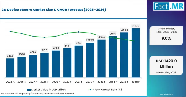
3d Device Ebeam Market Value Analysis | Source: Fact.MR
What are the defining numbers behind 3D Device eBeam Market growth?
USD 822.0 million absolute opportunity by 2036, led by Single-beam and Defect inspection alongside 3D NAND and Foundries.
- Demand Drivers in the Market
- Foundry process teams need electron-beam defect review when optical inspection misses nanoscale pattern faults in dense 3D layouts. Korea's Ministry of Trade, Industry and Resources reported in July 2026 that semiconductor exports rose 162.5% year on year in H1 2026 and semiconductors plus SSDs formed 83.7% of ICT exports.
- Memory makers require voltage contrast and buried-feature checks to protect channel integrity in 3D NAND stacks.
- Metrology groups need repeatable critical-dimension measurements as gate-all-around releases narrow tolerance windows.
- Packaging engineering teams use high-resolution review when advanced packages create die-shift, via-landing and bonding-risk checks. Singapore EDB reported in April 2025 that UMC's new 22 nm fab is due for volume production in 2026, lifting Singapore capacity above 1 million wafers annually.
- Key Segments Analyzed
- By Beam Configuration: Single-beam is expected to hold 41.0% share in 2026 since it remains the first qualification route for defect learning and recipe release.
- By Application: Defect inspection is projected to account for 37.0% share in 2026 as fabs need direct evidence of buried and surface defects before wafers move forward.
- By Device Architecture: 3D NAND is anticipated to capture 30.0% share in 2026 owing to deep channel structures that need voltage contrast and profile review.
- By End User: Foundries are estimated to represent 44.0% share in 2026 through mixed product flows and tight release checks across logic nodes.
- Analyst Opinion at Fact.MR
- Shambhu Nath Jha, Senior Consultant at Fact.MR, states, "3D device eBeam demand is less about adding another microscope and more about proving that small defects are found before wafers move to costly later steps. Supplier selection is expected to favor tools that combine clean images with fast defect review and stable measurement recipes. Fabs want inspection evidence that process engineers can defend during node release."
- Strategic Implications
- Tool vendors should document repeatability across 3D NAND and gate-all-around test wafers before commercial negotiations begin.
- Foundries should connect eBeam review data with optical inspection so sampling plans avoid unnecessary cycle time.
- Memory makers should define voltage-contrast acceptance rules early since buried opens and shorts carry high yield risk.
- Investors should separate direct 3D eBeam exposure from broader semiconductor inspection spending when assessing suppliers.
Taiwan is projected to record 10.82% CAGR through 2036 supported by foundry scale and advanced device qualification. South Korea is forecast to post 10.72% CAGR as memory makers use eBeam review for 3D NAND and HBM process control. The USA is anticipated to advance at 10.63% CAGR through CHIPS-linked fabs and metrology research. China is expected to reach 10.49% CAGR as local semiconductor output lifts process-control needs. Japan is estimated to post 10.40% CAGR through electron-optics depth and equipment capability. Singapore is projected to reach 10.34% CAGR as electronics manufacturing and wafer capacity expand.
How does the 3D Device eBeam Market break down by segment?
Single-beam leads Beam Configuration at 41.0% share in 2026. Defect inspection leads Application at 37.0% share in 2026.
Which beam configuration dominates?
Single-beam is projected to hold 41.0% share in 2026.
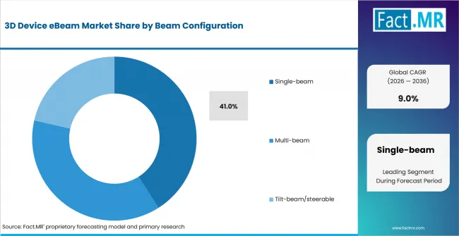
3d Device Ebeam Market Analysis By Beam Configuration | Source: Fact.MR
Single-beam tools lead the beam configuration segment because engineers rely on them for defect learning, recipe development, and detailed inspection. Their established use across qualified semiconductor processes also supports repeatable analysis, process tuning, and precise defect review.
What leads the Application segment?
Defect inspection is expected to account for 37.0% share in 2026.
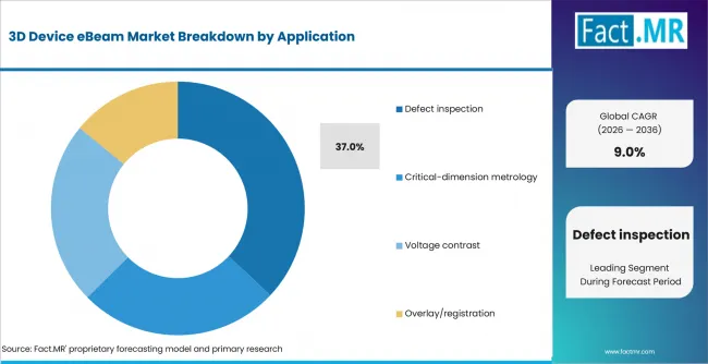
3d Device Ebeam Market Analysis By Application | Source: Fact.MR
It leads the application segment because advanced 3D semiconductor structures can contain hidden defects that optical systems may not resolve clearly. Electron-beam inspection supports detailed defect review, process control, and faster identification of critical manufacturing issues. NIST reported in April 2025 that SEM users need lower uncertainty when interpreting chip images, which supports eBeam use in defect review and CD checks.
How does Device Architecture shape demand?
3D NAND is anticipated to lead with 30.0% share in 2026.
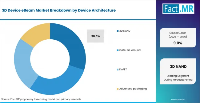
3d Device Ebeam Market Analysis By Device Architecture | Source: Fact.MR
3D NAND leads the device architecture segment because vertically stacked memory structures create complex inspection challenges that require high-resolution defect analysis. Electron-beam review helps identify buried defects, supports yield improvement, and provides detailed process evidence across advanced memory manufacturing.
What supports Foundries within End User?
Foundries are forecast to represent 44.0% share in 2026.
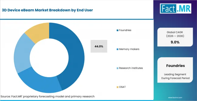
3d Device Ebeam Market Analysis By End User | Source: Fact.MR
Foundries lead the end-user segment because they manufacture a wide range of semiconductor devices for multiple customers, requiring consistent inspection and process monitoring. Electron-beam review supports defect analysis, recipe optimization, and production control across advanced logic, memory, and packaging technologies.
What is accelerating 3D Device eBeam Market adoption, and what is holding it back?
3D defect risk drives it; qualification cost restrains it.
Drivers Impact Analysis
| DRIVER | (~) % IMPACT ON CAGR | GEOGRAPHIC RELEVANCE | IMPACT TIMELINE |
|---|---|---|---|
| 3D NAND stack inspection | +2.4% | Taiwan, South Korea, China | Short term (<= 2 years) |
| Gate-all-around metrology | +2.0% | USA, Taiwan, Japan | Short term (<= 2 years) |
| Foundry process release | +1.8% | Taiwan, USA, Singapore | Medium term (2-4 years) |
| Voltage contrast checks | +1.5% | Memory clusters | Medium term (2-4 years) |
| Multi-beam throughput | +1.2% | Taiwan, South Korea, USA | Long term (>= 4 years) |
Source: Fact.MR analysis. Updated Aug 13, 2026
- 3D NAND stack inspection: Tall memory structures are expected to lift eBeam review needs because buried pattern failures are costly to find late. Suppliers that shorten defect review time gain a clearer path into memory fabs.
- Gate-all-around metrology: Gate-all-around devices require tight critical-dimension checks before process release.
- Foundry process release: Foundries are projected to keep the widest end-user share because mixed product flows need repeatable inspection recipes.
Opportunity Impact Analysis
| OPPORTUNITY | (~) % IMPACT ON CAGR | GEOGRAPHIC RELEVANCE | IMPACT TIMELINE |
|---|---|---|---|
| Multibeam inspection recipes | +1.1% | Taiwan, USA, Japan | Medium term (2-4 years) |
| AI-assisted SEM review | +0.9% | USA, Japan, Taiwan | Medium term (2-4 years) |
| Advanced packaging review | +0.8% | Singapore, Taiwan, USA | Long term (>= 4 years) |
| Domestic process support | +0.7% | China, South Korea, Japan | Long term (>= 4 years) |
Source: Fact.MR analysis. Updated Aug 13, 2026
- Multibeam inspection recipes: Multibeam eBeam inspection creates opportunity where fabs need more sites per wafer without extending review queues. Image quality still decides production acceptance.
- AI-assisted SEM review: AI-assisted SEM image review is expected to help process teams screen complex defect patterns faster. The opportunity is concentrated where review data links to yield learning.
- Advanced packaging review: Advanced packaging adds a route for eBeam tools when fine features and bonding surfaces need high-resolution confirmation.
Restraints Impact Analysis
| RESTRAINT | (~) % IMPACT ON CAGR | GEOGRAPHIC RELEVANCE | IMPACT TIMELINE |
|---|---|---|---|
| Export control exposure | -1.2% | China and global suppliers | Short term (<= 2 years) |
| Tool cost and qualification time | -1.0% | Global | Short term (<= 2 years) |
| Charging and beam damage risk | -0.8% | Logic and memory fabs | Medium term (2-4 years) |
| Specialist service bottlenecks | -0.6% | Emerging fab clusters | Long term (>= 4 years) |
Source: Fact.MR analysis. Updated Aug 13, 2026
- Export control exposure: Export controls restrain some cross-border eBeam placements because advanced inspection tools are tied to semiconductor manufacturing capability. Licensing complexity can slow purchase timing.
- Tool cost and qualification time: EBeam systems require long acceptance work before regular production use. Smaller lines are expected to delay purchases until utilization is clearer.
- Charging and beam damage risk: Dense 3D devices can be sensitive to charging and beam effects during inspection. Process teams therefore need evidence that review settings do not damage the feature being measured.
Which countries are scaling 3D Device eBeam Market fastest?
- The country comparison spans 0.48 percentage point and forms one tight growth band across the forecast period.
- Taiwan remains 0.10 percentage point above South Korea through foundry scale and advanced-node qualification.
- South Korea remains 0.09 percentage point above the USA as memory production supports voltage contrast and defect review.
- The USA remains 0.14 percentage point above China through CHIPS-linked capacity and semiconductor metrology research.
- Japan remains 0.06 percentage point above Singapore through electron-optics capability and semiconductor equipment depth.
- Singapore closes the displayed range through electronics manufacturing and nearby wafer-capacity expansion.
Comparable CAGRs create different entry conditions due to fab scale, qualification requirements and local engineering depth. Full report coverage includes North America, Latin America, Europe, East Asia, South Asia and Pacific, Middle East and Africa.
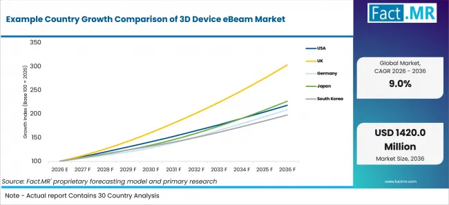
Example Country Growth Comparison Of 3d Device Ebeam Market | Source: Fact.MR
| COUNTRY | CAGR (2026-2036) |
|---|---|
| Taiwan | 10.82% |
| South Korea | 10.72% |
| USA | 10.63% |
| Japan | 10.40% |
| Singapore | 10.34% |
Source: Fact.MR analysis. Updated Aug 13, 2026
What supports Taiwan adoption?
10.82% CAGR, supported by foundry scale and advanced-node inspection demand.
Taiwan’s growth reflects a market where foundries must prove 3D device quality before wafers move deeper into production. The Ministry of Economic Affairs reported in May 2026 that Q1 electronic components output reached NT$2.1779 trillion and grew 25.29. Taiwan’s 25.8% country share is expected to keep eBeam qualification close to high-volume foundry and memory programs.
How is South Korea scaling demand?
10.72% CAGR, driven by memory manufacturing and voltage-contrast review.
South Korea’s growth is tied to memory makers that need defect review across 3D NAND, DRAM and HBM process steps. South Korea’s 22.1% country share is expected to support steady tool demand around memory yield learning.
What supports USA growth?
10.63% CAGR, supported by fab investment and SEM metrology research.
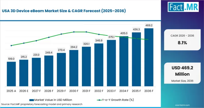
3d Device Ebeam Market Country Value Analysis | Source: Fact.MR
The USA’s growth reflects a market where process-control tools must prove their value during long fab ramp cycles. The USA’s 18.7% country share is expected to benefit where leading-edge logic and packaging programs require defensible eBeam evidence. NIST reported in January 2025 an award of up to USD 6.3 billion over 10 years for Natcast to operate the National Semiconductor Technology Center.
How does Japan perform?
10.40% CAGR, led by electron-optics capability and equipment depth.
Japan’s growth reflects its established metrology base and close coordination between process engineering and equipment suppliers. Japan’s 10.9% country share is expected to stay linked to high-resolution CD-SEM and defect-review capability.
What supports Singapore’s growth?
10.34% CAGR, backed by electronics manufacturing depth and wafer-capacity expansion.
Singapore’s growth reflects a compact semiconductor cluster where fabs, OSATs and service teams operate close to one another. The Economic Development Board reported in February 2026 that 2025 fixed asset investment reached S$14.2 billion, including about S$12.1 billion from manufacturing-related projects. Singapore’s 8.1% country share is expected to track selective demand for inspection recipes and field support.
Who leads the 3D Device eBeam Market?
ASML (HMI) and Applied Materials show the clearest direct relevance, while Hitachi High-Tech, KLA, JEOL LTD. and ZEISS Semiconductor Manufacturing Technology (ZEISS SMT) strengthen the wider electron-beam inspection and metrology field.
ASML (HMI) supports single-beam and multibeam inspection within broader lithography control. In March 2025, ASML and imec announced a strategic partnership that includes 0.55 NA EUV, 0.33 NA EUV, YieldStar optical metrology and HMI single- and multi-beam technologies. Hitachi High-Tech supports CD-SEM and metrology SEM use, while KLA remains relevant through defect inspection and review systems. JEOL LTD. and ZEISS Semiconductor Manufacturing Technology (ZEISS SMT) extend the field through electron-beam and SEM capabilities.
Which companies are the key providers?
Key companies include ASML (HMI), Applied Materials, Hitachi High-Tech, KLA, JEOL LTD. and ZEISS Semiconductor Manufacturing Technology (ZEISS SMT).
- ASML (HMI)
- Applied Materials
- Hitachi High-Tech
- KLA
- JEOL LTD.
- ZEISS Semiconductor Manufacturing Technology (ZEISS SMT)
Bibliography
- Applied Materials, Inc. (2025, October 7). Applied Materials unveils next-gen chipmaking products to supercharge AI performance.
- ASML Holding N.V. (2025, March 11). ASML and imec sign strategic partnership agreement to support semiconductor research and sustainable innovation in Europe.
- Singapore Economic Development Board. (2026, February 9). EDB Year 2025 in Review.
- Ministry of Economic Affairs, R.O.C. (2026, May 19). 115年第1季製造業產值統計 [Manufacturing production value statistics for the first quarter of 2026].
- Ministry of Trade, Industry and Resources, & Ministry of Science and ICT. (2026, January 15). ICT exports post record annual performance in 2025.
- National Institute of Standards and Technology. (2025, April 25). NIST study aims to improve utility of the scanning electron microscope.
- U.S. Government Accountability Office. (2025, December 11). Semiconductors: Information on projects funded to strengthen U.S. supply chain (GAO-26-107882).
- Ministry of Trade, Industry and Resources, & Ministry of Science and ICT. (2026, July 14). Korea’s ICT exports reach record $253.9 billion in first half of 2026.
This Report Answers
- The report provides strategic intelligence on the 3D Device eBeam Market across Beam Configuration and Application choices that shape semiconductor inspection programs.
- Segment analysis covers Single-beam systems and Defect inspection as the share leaders within the 2026 market.
- Country outlook evaluates Taiwan and South Korea alongside the USA and China. Japan and Singapore complete the growth comparison across the profiled markets.
- Competitive analysis profiles ASML (HMI) and Applied Materials alongside Hitachi High-Tech and KLA. JEOL LTD. and ZEISS Semiconductor Manufacturing Technology (ZEISS SMT) complete the provider set.
- Process-control assessment covers eBeam defect review, critical-dimension metrology, voltage contrast and overlay or registration work for three-dimensional devices.
What does the 3D Device eBeam Market cover?
The 3D Device eBeam Market covers equipment used for high-resolution inspection and measurement of three-dimensional semiconductor devices. Coverage includes e-beam wafer inspection systems, defect inspection and CD metrology where electron-beam imaging supports process release.
The market includes single-beam and multibeam systems used in foundries, memory fabs, research institutes and OSAT environments. Coverage applies when the tool is used to examine 3D NAND, gate-all-around, FinFET or advanced packaging structures.
What is included in the scope?
The scope includes Beam Configuration, Application, Device Architecture and End User. It also includes adjacent process-control needs such as semiconductor defect inspection equipment when the use case is tied to 3D device review.
Coverage spans single-beam, multibeam and tilt-beam tools across defect inspection, critical-dimension metrology, voltage contrast and overlay or registration. It includes systems used for wafer-level recipe qualification and production release.
What is excluded from the scope?
General optical inspection, standalone lithography and broad semiconductor capital equipment remain outside the scope unless they directly support eBeam review of 3D devices. Related areas such as 3D semiconductor packaging are included only when electron-beam inspection or metrology is part of the process-control requirement.
The scope excludes company revenue without a clear connection to eBeam inspection or metrology. It also excludes general microscopy used outside semiconductor manufacturing.
How Was the Analysis Built?
The analysis draws on 120+ sources, 35+ company portfolios, 25+ countries, and 20+ industry interviews.
- Primary Research: Primary research includes discussions with equipment suppliers, process engineers, foundry teams, memory makers, OSAT users and subject-matter experts. These conversations examine purchasing priorities, approval requirements and service constraints.
- Desk Research: Desk research covers government statistics, company filings, official technology launches, public policy, equipment associations and standards. Every source used in the analysis is documented in the bibliography.
- Market Sizing and Forecasting: Market estimates combine historical performance, segment shares, company participation, country growth, adoption patterns, investment activity and expansion barriers.
- Data Validation and Update Cycle: Findings are validated by comparing interviews with public data, company activity, regulatory changes and equipment developments. Regular updates review launches, partnerships and shifts in commercial adoption.
Segmentation
What is the report’s scope and coverage?
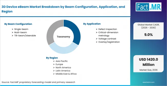
3d Device Ebeam Market Breakdown By Beam Configuration, Application, And Region | Source: Fact.MR
| Attribute | Details |
|---|---|
| Quantitative Units | USD million in 2026 to USD million by 2036 at CAGR |
| Market Definition | Electron-beam inspection, metrology, defect review and voltage contrast systems used for three-dimensional semiconductor devices where high-resolution evidence supports yield learning and process release |
| Beam Configuration | Single-beam; Multi-beam; Tilt-beam/steerable |
| Application | Defect inspection; Critical-dimension metrology; Voltage contrast; Overlay/registration |
| Device Architecture | 3D NAND; Gate-all-around; FinFET; Advanced packaging |
| End User | Foundries; Memory makers; Research institutes; OSAT |
| Regions Covered | North America; Latin America; Europe; East Asia; South Asia and Pacific; Middle East and Africa |
| Countries Covered | Taiwan; South Korea; USA; Japan; Singapore |
| Key Companies Profiled | ASML (HMI); Applied Materials; Hitachi High-Tech; KLA; JEOL LTD.; ZEISS Semiconductor Manufacturing Technology (ZEISS SMT) |
| Forecast Period | 2026 to 2036 |
| Approach | Hybrid top-down and bottom-up approach using semiconductor inspection demand; 3D NAND and gate-all-around process requirements; defect review needs; voltage contrast use; wafer-level metrology; country adoption patterns and company portfolio review |
Source: Fact.MR analysis. Updated Aug 13, 2026
How is the market segmented?
-
By Beam Configuration
- Single-beam
- Multi-beam
- Tilt-beam/steerable
-
By Application
- Defect inspection
- Critical-dimension metrology
- Voltage contrast
- Overlay/registration
-
By Device Architecture
- 3D NAND
- Gate-all-around
- FinFET
- Advanced packaging
-
By End User
- Foundries
- Memory makers
- Research institutes
- OSAT
-
By Region
- North America
- Latin America
- Western Europe
- Eastern Europe
- East Asia
- South Asia and Pacific
- Middle East & Africa
Frequently Asked Questions
How big is the 3D Device eBeam market in 2026?
What is the CAGR of the 3D Device eBeam market from 2026 to 2036?
Which beam configuration leads the 3D Device eBeam market?
Which application leads the 3D Device eBeam market?
Who are the leading companies in the 3D Device eBeam market?
Who worked on this report


Preview the report firsthand - request a free sample
Free SampleGet the brochure for pricing and purchase details
Download PDF