- Market Value (2025): USD 114.1 Mn
- Estimated Value (2026): USD 131.0 Mn
- Forecast Value (2036): USD 520.0 Mn
- CAGR (2026-2036): 14.8%
What is the Additive Solder Mask Market forecast to be worth by 2036?
USD 131 million in 2026 and forecasts USD 520 million by 2036, implying a 14.8% CAGR.
- The Additive Solder Mask Market at USD 114.1 million in 2025.
- Demand is projected to increase from USD 131.0 million in 2026 to USD 520.0 million by 2036.
- The market is forecast to record 14.8% CAGR from 2026 to 2036 as substrate makers and PCB fabricators qualify finer solder-mask openings around denser interconnect designs.
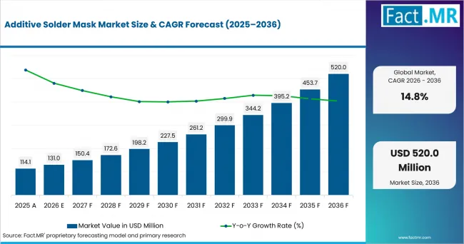
Additive Solder Mask Market Value Analysis | Source: Fact.MR
What are the defining numbers behind Additive Solder Mask Market growth?
Absolute opportunity is USD 389 million by 2036.
- Demand Drivers in the Market
- Substrate makers need additive coating routes that protect fine copper traces while keeping solder-mask thickness uniform across panels.
- PCB fabricators require imageable chemistry that opens smaller pads cleanly because HDI boards leave less tolerance for registration error.
- OSAT and packaging teams value solder-mask materials that lower assembly risk around package substrates exposed to repeated heat cycles.
- China’s Ministry of Industry and Information Technology reported that major companies in China’s electronic information manufacturing sector generated RMB 17.4 trillion in operating revenue in 2025, up 7.4% year over year.
- Key Segments Analyzed
- By Material System: Photo-imageable additive is expected to hold 42.0% share in 2026 due to its fit with fine openings and stable development behavior.
- By Substrate Target: IC substrates are projected to account for 38.0% share in 2026 owing to tight pad geometry and advanced packaging qualification needs.
- By End User: Substrate makers are anticipated to capture 44.0% share in 2026 as package-substrate lines carry the strictest release requirements.
- Analyst Opinion at Fact.MR
- Shambhu Nath Jha, Principal Consultant at Fact.MR, states, "Additive solder mask is drawing attention because the mask layer now affects package yield and final assembly reliability. Supplier acceptance is expected to depend on cleaner openings and proof that the same material works across fine-pitch substrates. Winning vendors should combine chemistry control, application support and documentation that helps engineering teams shorten approval cycles."
- Strategic Implications
- Substrate makers should test solder-mask opening quality against the copper-pillar and pad geometries used in their next package platforms.
- PCB fabricators should keep process windows narrow enough to reduce rework when HDI designs move from prototype to routine production.
- Material suppliers should support customers with exposure, development and cure data that can be audited during line qualification.
- NIST reported on January 16, 2025 that CHIPS NAPMP finalized USD 1.4 billion in advanced-packaging awards, including USD 300 million for advanced-substrate and materials research and USD 1.1 billion for the Natcast advanced-packaging piloting facility.
Japan leads at 16.50% CAGR through package-substrate expertise and local semiconductor policy. China follows at 16.42% as integrated-circuit output and PCB manufacturing scale support demand. South Korea reaches 16.33% through memory exports and package-reliability requirements. Taiwan records 16.32% through foundry-linked substrates and electronics production. The USA posts 16.18% through advanced-packaging R&D and substrate pilots, while Germany reaches 16.14% through semiconductor investment and EU-linked compliance needs.
How does the Additive Solder Mask Market break down by segment?
Photo-imageable additive leads at 42.0%; IC substrates lead at 38.0%.
Which material system dominates?
Photo-imageable additive is projected to account for 42.0% share in 2026.
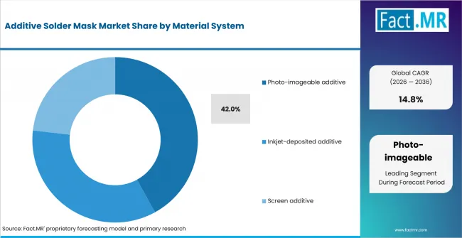
Additive Solder Mask Market Analysis By Material System | Source: Fact.MR
Photo-imageable additive leads the Material System segment because it gives process teams precise control over exposed and developed openings, supporting cleaner pattern definition and tighter solder-mask placement for increasingly dense PCB and package-substrate designs during qualification.
What leads the Substrate Target segment?
IC substrates are expected to hold 38.0% share in 2026.
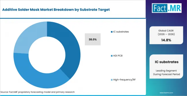
Additive Solder Mask Market Analysis By Substrate Target | Source: Fact.MR
IC substrates lead the Substrate Target segment because package-substrate lines require tighter pad openings and stronger process proof before volume release. Their fine-pitch geometry increases the importance of accurate solder-mask definition, adhesion and reliable processing during advanced packaging qualification.
How does End User shape demand?
Substrate makers are anticipated to hold 44.0% share in 2026.
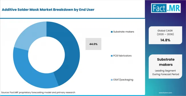
Additive Solder Mask Market Analysis By End User | Source: Fact.MR
Substrate makers lead the End User segment because package-substrate production carries strict release requirements for fine solder-mask openings, adhesion and reliability. Their advanced manufacturing lines require precise process control and consistent material performance before volume production, supporting stronger adoption of additive solder-mask systems.
What is accelerating Additive Solder Mask Market adoption, and what is holding it back?
IC substrate density drives it; qualification cost restrains it.
Drivers Impact Analysis
| DRIVER | (~) % IMPACT ON CAGR | GEOGRAPHIC RELEVANCE | IMPACT TIMELINE |
|---|---|---|---|
| IC substrate density | +3.8% | Japan, Taiwan, China | Short term (<= 2 years) |
| HDI PCB miniaturization | +3.0% | China, South Korea, Taiwan | Short term (<= 2 years) |
| Photo-imageable process control | +2.5% | Japan, USA, Germany | Medium term (2-4 years) |
| Low-substance formulations | +1.9% | Europe, USA, Japan | Medium term (2-4 years) |
| Packaging R&D support | +1.4% | USA, Japan, Germany | Long term (>= 4 years) |
Source: Fact.MR analysis. Updated Aug 14, 2026
- IC substrate density: Fine-pitch substrates require solder-mask openings that stay clean after exposure and development. Package engineers treat mask defects as yield risks because small errors can spread into assembly and reliability testing.
- HDI PCB miniaturization: HDI fabricators need finer solder dams and better registration around dense via structures. Additive mask routes help reduce excess coating and support local pattern control. Demand is projected to strengthen where smartphones, servers and vehicle electronics use smaller pads.
- Photo-imageable process control: Photo-imageable systems give fabricators a familiar approval path while improving opening definition. Materials that hold viscosity, exposure response and development tolerance reduce the number of trial runs. The segment is expected to keep its position when customers prefer qualification certainty.
- Low-substance formulations: Compliance teams screen solder-mask inputs against restricted-substance lists before approving new materials. Reformulated products are anticipated to gain attention where customers need safer chemistry without changing every line condition. Suppliers must still prove adhesion and heat resistance.
- Packaging R&D support: Public funding for advanced packaging raises the need for substrate materials that can be tested at pilot scale. Additive solder mask is projected to benefit when pilot lines move from material screening into repeatable substrate processes. The timing depends on customer design rules.
Opportunity Impact Analysis
| OPPORTUNITY | (~) % IMPACT ON CAGR | GEOGRAPHIC RELEVANCE | IMPACT TIMELINE |
|---|---|---|---|
| Dry-film package solder resist | +1.6% | Japan, Taiwan, South Korea | Medium term (2-4 years) |
| Inkjet additive deposition | +1.2% | China and Europe | Medium term (2-4 years) |
| High-frequency board materials | +0.9% | USA, Germany, Japan | Long term (>= 4 years) |
| Compliance-led reformulation | +0.7% | Europe and export PCB hubs | Long term (>= 4 years) |
Source: Fact.MR analysis. Updated Aug 14, 2026
- Dry-film package solder resist: Film formats give substrate makers better thickness control when package surfaces become less tolerant of uneven coating.
- Inkjet additive deposition: Inkjet deposition reduces mask placement outside required areas and allows fabricators to test lower-waste coating. Adoption is expected to remain selective until viscosity control and line uptime are proven. The clearest fit is in designs with frequent pattern changes.
- High-frequency board materials: RF boards need mask materials that do not disrupt signal behavior around dense conductive paths. Additive solder mask is anticipated to gain attention where fabricators already qualify low-loss laminates and controlled surface finishes. The opportunity depends on stable dielectric behavior under customer tests.
- Compliance-led reformulation: Restrictions on substances of concern create a route for newer photoinitiator and resin packages. European customers often require documentation before approving materials for export-oriented PCB production. Reformulation is projected to support premium pricing where suppliers combine safer chemistry with reliable processing.
Restraints Impact Analysis
| RESTRAINT | (~) % IMPACT ON CAGR | GEOGRAPHIC RELEVANCE | IMPACT TIMELINE |
|---|---|---|---|
| Qualification cycle length | -1.4% | Global substrate makers | Short term (<= 2 years) |
| Deposition uniformity risk | -1.0% | IC substrate and HDI lines | Short term (<= 2 years) |
| Restricted chemistry transition | -0.8% | Europe-linked supply chains | Medium term (2-4 years) |
| Capital and skill burden | -0.6% | Smaller PCB fabricators | Long term (>= 4 years) |
Source: Fact.MR analysis. Updated Aug 14, 2026
- Qualification cycle length: Additive solder mask cannot move into production without exposure, development and reliability proof. Each substrate design can force new evidence on adhesion and opening shape. Smaller customers are expected to delay conversion when qualification time exceeds the benefit from lower material waste.
- Deposition uniformity risk: Inkjet and screen routes must control local thickness and edge definition across the panel. Defects raise rework cost when the mask is close to fine copper features. Wider adoption is forecast to depend on tighter process monitoring and stable cleaning routines.
- Restricted chemistry transition: Chemical reformulation can alter cure response and final reliability. Suppliers must prove that lower-substance systems still match the old process window. Adoption is anticipated to slow when compliance files are ready before production teams trust the new material.
- Capital and skill burden: Direct deposition and advanced imaging can require new equipment settings and operator training. Plants that run mature multilayer PCBs often avoid line changes unless customers pay for tighter mask control.
Which countries are scaling Additive Solder Mask Market fastest?
- The country comparison spans 0.36 percentage point and forms three practical growth bands across the forecast period.
- Japan remains 0.08 percentage point above China through package-substrate expertise and local semiconductor policy.
- China remains 0.09 percentage point above South Korea as integrated-circuit output and PCB manufacturing scale support demand.
- South Korea remains 0.01 percentage point above Taiwan through memory exports and package-reliability requirements.
- Taiwan remains 0.14 percentage point above the USA through foundry-linked substrates and electronics production.
- The USA remains 0.04 percentage point above Germany through advanced-packaging R&D and substrate-pilot activity.
Comparable CAGRs can create different entry conditions due to package-substrate scale, qualification requirements, electronics manufacturing depth and local policy support. Full report coverage includes North America, Latin America, Europe, East Asia, South Asia and Pacific, Middle East and Africa.
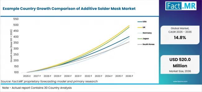
Example Country Growth Comparison Of Additive Solder Mask Market | Source: Fact.MR
| Country | CAGR (2026-2036) |
|---|---|
| Japan | 16.50% |
| South Korea | 16.33% |
| Taiwan | 16.32% |
| USA | 16.18% |
| Germany | 16.14% |
Source: Fact.MR analysis. Updated Aug 14, 2026
What supports Japan adoption?
16.50% CAGR, supported by package-substrate know-how and local semiconductor policy.
Japan’s 16.50% CAGR is supported by package-substrate know-how and domestic semiconductor policy. METI selected Rapidus for financial support on November 21, 2025 and stated that it intended to invest JPY 100.0 billion, allocated in the fiscal 2025 initial budget, in Rapidus through IPA. This policy support strengthens the local semiconductor ecosystem and provides a supportive environment for advanced substrate materials and additive solder-mask qualification.
How is South Korea developing demand?
16.33% CAGR, supported by memory exports and package-reliability pressure.
South Korea’s 16.33% CAGR is supported by memory exports and package-reliability pressure. Korea’s Ministry of Trade, Industry and Resources and Ministry of Science and ICT reported on January 15, 2026 that semiconductor exports increased 22.1% year over year in 2025. Strong semiconductor export activity supports continued package and substrate production, where reliable solder-mask performance and precise openings remain important during qualification and volume manufacturing.
What is driving Taiwan’s growth from 2026 to 2036?
16.32% CAGR, backed by foundry-linked substrates and electronics production.
Taiwan’s 16.32% CAGR is backed by foundry-linked substrates and expanding electronics production. DGBAS reported on May 28, 2025 that Taiwan’s manufacturing sector grew 11.03% year over year in 2025Q1, mainly because of output expansion in semiconductors, computers, electronics and optical products. This manufacturing momentum supports demand for advanced substrate materials and precise additive solder-mask systems used in dense electronic and semiconductor packaging applications.
What supports USA adoption?
16.18% CAGR, supported by advanced packaging R&D and substrate pilots.
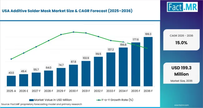
Additive Solder Mask Market Country Value Analysis | Source: Fact.MR
The USA’s 16.18% CAGR is supported by advanced packaging R&D and substrate pilot activity. NIST reported in January 2025 that CHIPS NAPMP finalized USD 1.4 billion in advanced-packaging awards, including USD 300 million for advanced substrates and material research and USD 1.1 billion to Natcast to operate the advanced-packaging capabilities of the NSTC Prototyping and NAPMP Advanced Packaging Piloting Facility. These investments support material testing, process development and qualification for advanced packaging and substrate technologies.
How does Germany perform?
16.14% CAGR, led by semiconductor investment and EU-linked compliance needs.
Germany’s 16.14% CAGR is led by semiconductor investment and EU-linked compliance needs. The European Commission’s Representation in Germany reported on February 20, 2025 that the Commission approved a EUR 920.0 million German State-aid measure for a new Infineon semiconductor manufacturing facility in Dresden. This investment strengthens local semiconductor manufacturing capacity and supports demand for qualified electronic materials, including advanced substrate and solder-mask solutions.
Who leads the Additive Solder Mask Market?
Competitive set includes Taiyo Ink Mfg. Co., Ltd., Electra Polymers, Lackwerke Peters, Agfa-Gevaert. Official company sources confirm relevant solder-resist, PCB, package-substrate or interconnect product portfolios.
Taiyo Ink Mfg. Co., Ltd. lists solder-resist products for rigid PCBs and package substrates. Electra Polymers lists IC-substrate interconnect and dry-film photoresist solutions.
Which companies are the key providers?
Key companies include Taiyo Ink Mfg. Co., Ltd., Electra Polymers, Lackwerke Peters, Agfa-Gevaert.
- Taiyo Ink Mfg. Co., Ltd.
- Electra Polymers
- Lackwerke Peters
- Agfa-Gevaert
Bibliography
- Directorate General of Budget, Accounting and Statistics, Executive Yuan. (2025, May 28). GDP: Preliminary estimate for 2025Q1, and outlook for 2025.
- European Commission. (2025, February 20). Commission approves €920 million German State aid measure to support Infineon in setting up a new semiconductor manufacturing facility.
- Ministry of Economy, Trade and Industry. (2025, November 21). Press conference by Minister Akazawa (Excerpt).
- Ministry of Trade, Industry and Resources. (2026, January 15). ICT exports post record annual performance in 2025.
- National Institute of Standards and Technology. (2025, January 16). U.S. Department of Commerce announces $1.4 billion in final awards to support the next generation of U.S. semiconductor advanced packaging.
This Report Answers
- The report provides strategic intelligence on photo-imageable systems and additive deposition routes.
- Segment analysis covers IC substrates and organic substrate use cases.
- Country outlook evaluates Japan, China, South Korea, Taiwan, the USA and Germany for semiconductor substrates.
- Competitive analysis profiles Taiyo Ink Mfg. Co., Ltd., Electra Polymers, Lackwerke Peters, Agfa-Gevaert in electronic chemicals.
- Process assessment connects imageable coating and deposition control with advanced packaging qualification.
- End-user analysis examines substrate makers, PCB fabricators and OSAT teams using printed circuit materials.
- The scope separates additive solder mask from dispensing robots, solder paste and unrelated chemistry.
- The forecast links material qualification to semiconductor process needs and package-substrate scale.
- The analysis reviews how active electronic production influences customer approvals.
- Adjacent packaging review includes embedded bridge requirements that raise material documentation needs.
What does the Additive Solder Mask Market cover?
Additive solder mask materials form protective dielectric layers on PCB and package-substrate surfaces. The market covers photo-imageable, inkjet-deposited and screen-applied systems where material behavior affects copper protection and reliability.
The Additive Solder Mask Market covers materials used on IC substrates, HDI PCBs and high-frequency or RF boards. Coverage extends to substrate makers, PCB fabricators and OSAT or packaging operations.
What is included in the scope?
The scope includes additive solder mask materials used in commercial board and substrate manufacturing. Material System, Substrate Target and End User form the main segmentation. IC substrates, HDI PCBs and high-frequency/RF targets follow the market-use rule.
What is excluded from the scope?
General solder paste, solder flux and unrelated PCB process chemistry remain outside the scope. Standard coatings that do not function as solder mask are excluded. Company revenue without a solder-mask connection is also excluded.
How Was the Analysis Built?
The analysis draws on 120+ sources, 35+ company portfolios, 25+ countries, and more than 20 industry interviews.
- Primary Research: Primary research includes discussions with manufacturers, service providers, technology developers, distributors, end users, procurement teams, and subject-matter experts. These conversations examine purchasing priorities, product adoption, operational challenges, approval requirements, competitive positioning, and the factors that influence wider market acceptance.
- Desk Research: Desk research covers government statistics, regulatory publications, company filings, trade data, technical studies, industry associations, standards, public policy, and other authoritative sources. Every source used in the analysis is documented in the bibliography.
- Market Sizing and Forecasting: Market estimates combine historical performance, demand indicators, pricing and volume trends, segment shares, company participation, country-level growth, adoption patterns, investment activity, and barriers to market expansion.
- Data Validation and Update Cycle: Findings are validated by comparing primary interviews with public data, company activity, regulatory changes, trade patterns, and industry developments. Regular updates review new product launches, capacity changes, partnerships, approvals, procurement trends, and shifts in commercial adoption.
Segmentation
What is the report’s scope and coverage?
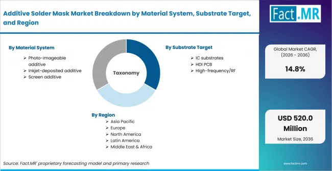
Additive Solder Mask Market Breakdown By Material System, Substrate Target, And Region | Source: Fact.MR
| Attribute | Details |
|---|---|
| Quantitative Units | USD million |
| Market Definition | Additive solder mask materials used to form protective dielectric layers on PCB and IC substrate surfaces where opening accuracy, copper protection, adhesion and cure behavior determine process qualification and production release |
| Material System | Photo-imageable additive; Inkjet-deposited additive; Screen additive |
| Substrate Target | IC substrates; HDI PCB; High-frequency/RF |
| End User | Substrate makers; PCB fabricators; OSAT/packaging |
| Regions Covered | North America; Latin America; Europe; East Asia; South Asia and Pacific; Middle East and Africa |
| Countries Covered | Japan; China; Taiwan; South Korea; USA; Germany |
| Key Companies Profiled | Taiyo Ink Mfg. Co., Ltd.; Electra Polymers; Lackwerke Peters; Agfa-Gevaert |
| Forecast Period | 2026 to 2036 |
| Approach | Hybrid top-down and bottom-up approach using PCB materials demand; package-substrate qualification activity; additive deposition routes; HDI board adoption; electronics manufacturing statistics; country adoption patterns; company portfolio review; regulatory screening; and supplier validation |
Source: Fact.MR analysis. Updated Aug 14, 2026
How is the market segmented?
-
By Material System
- Photo-imageable additive
- Inkjet-deposited additive
- Screen additive
-
By Substrate Target
- IC substrates
- HDI PCB
- High-frequency/RF
-
By End User
- Substrate makers
- PCB fabricators
- OSAT/packaging
-
By Region
- North America
- Latin America
- Europe
- East Asia
- South Asia and Oceania
- Middle East and Africa
Frequently Asked Questions
How big is the additive solder mask market in 2026?
What is the CAGR of the additive solder mask market from 2026 to 2036?
Which material system leads the additive solder mask market?
Which substrate target leads the additive solder mask market?
Who are the leading companies in the additive solder mask market?
Who worked on this report


Preview the report firsthand - request a free sample
Free SampleGet the brochure for pricing and purchase details
Download PDF