- Market Value (2025): USD 296.1 Mn
- Estimated Value (2026): USD 317.2 Mn
- Forecast Value (2036): USD 633.5 Mn
- CAGR (2026-2036): 7.2%
What is the Electron Beam Lithography Market forecast to be worth by 2036?
USD 317.3 million in 2026 to USD 633.5 million by 2036 at a 7.2% CAGR.
- As per Fact.MR analysis, the electron beam lithography market was valued at USD 296.1 million in 2025
- Demand will grow from USD 317.2 million in 2026 to USD 633.5 million by 2036.
- The forecast records a 7.2% CAGR from 2026 to 2036 as semiconductor research, nanofabrication and demand for high-resolution direct-write patterning support system adoption.
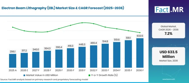
Electron Beam Lithography Ebl Market Forecast Global | Source: Fact.MR
| Year | Basis | Market Value (USD million) |
|---|---|---|
| 2025 | Actual | 296.1 |
| 2026 | Estimate | 317.2 |
| 2036 | Forecast | 633.5 |
| CAGR 2026 to 2036 | Forecast period | 7.2% |
Source: Fact.MR analysis. Updated Nov 4, 2026
What are the defining numbers behind Electron Beam Lithography Market growth?
USD 316.2 million absolute opportunity between 2026 and 2036.
- Demand Drivers in the Market
- Advanced semiconductor development supports demand for precision lithography equipment. The Semiconductor Industry Association reported that global semiconductor sales reached USD 791.7 billion in 2025, an increase of 25.6% over 2024. [3]
- Growing interest in quantum and photonic devices creates opportunities for high-resolution patterning. The U.S. National Institute of Standards and Technology identifies electron beam lithography as an important capability for fabricating nanostructures used in quantum photonic integrated circuits, optical devices and nanoscale sensors. These research areas require accurate pattern placement and fine feature control. [1]
- Expansion of semiconductor research infrastructure supports equipment investment. Governments and research institutions are strengthening domestic semiconductor capabilities through funding, infrastructure programmes and technology development. Brazil's Brasil Semicon programme supports research, development, innovation, design and production across the semiconductor ecosystem. Such initiatives can create opportunities for EBL equipment suppliers serving universities, research centres and specialized manufacturers. [4]
- Key Segments Analyzed
- By Type: Thermionic Sources will account for 52.5% of the market in 2026, supported by their use in electron-beam generation across lithography systems.
- By Application: Electronic Field lead with a 42.5% share in 2026, reflecting the role of EBL in semiconductor-related patterning and advanced electronic device development.
- Analyst Opinion at Fact.MR
- Shambhu Nath Jha, Principal Consultant at Fact.MR, states, “Demand for electron beam lithography systems will depend on the need for precise patterning in advanced semiconductor research and emerging nanotechnology applications. Equipment providers that combine high-resolution writing with stable operation and practical throughput can strengthen their position among research institutions and specialized manufacturers.”
- Strategic Implications
- EBL system manufacturers should improve beam stability, pattern placement accuracy and automation to address increasingly demanding nanofabrication requirements.
- Equipment suppliers need to provide application-specific configurations for semiconductor research, photonics, quantum devices and industrial patterning.
- Research institutions must evaluate system resolution, substrate compatibility and operating costs before investing in high-value lithography equipment.
- Suppliers need to strengthen application support and training to help laboratories optimize exposure conditions and improve process repeatability.
- Manufacturers can expand their customer base by developing systems that balance high-resolution patterning with throughput and ease of operation.
Germany is set to record 8.1% CAGR through 2036. Brazil is set to post 7.4%, followed by the USA at 6.7%. The UK is estimated to advance at 6.0%, while Japan is forecast at 5.3%.
How does the Electron Beam Lithography Market break down by segment?
Fact.MR finds that Thermionic Sources leads Type at 52.5%, while Electronic Field Leads Application at 42.5%.
Which Type dominates?
Thermionic Sources is set to hold 52.5% share in 2026.
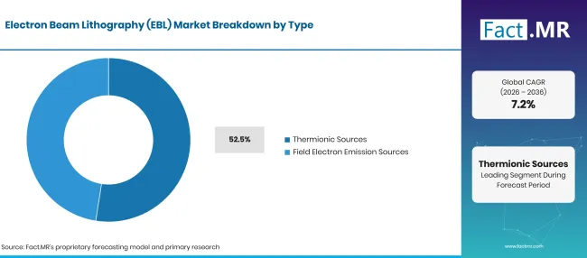
Electron Beam Lithography Ebl Market Breakdown Type | Source: Fact.MR
| Type | Share (2026) |
|---|---|
| Thermionic Sources (Leading segment) | 52.5% |
| Other segments combined | 47.5%* |
| Total | 100.0% |
Source: Fact.MR analysis. Updated Nov 4, 2026
Thermionic sources account for the leading type share under the market segmentation. These electron sources generate electrons through heating and are used in electron-beam equipment designs where source characteristics and operating requirements determine system performance. Field electron emission sources form the other major category. They are relevant to systems requiring high-brightness electron beams and fine patterning capabilities. Equipment buyers evaluate source technology according to beam current, brightness, resolution and maintenance requirements.
What leads the Application segment?
Electronic Field is set to represent 42.5% share in 2026.
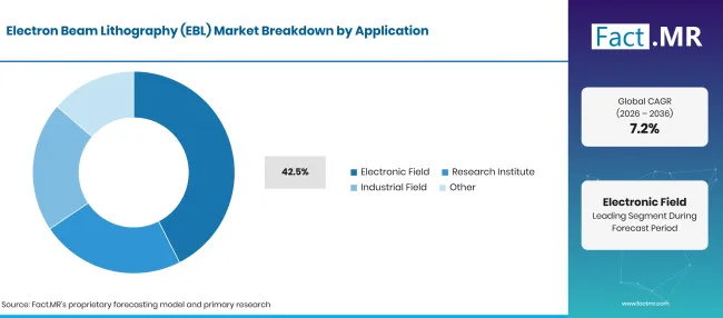
Electron Beam Lithography Ebl Market Breakdown Application | Source: Fact.MR
| Application | Share (2026) |
|---|---|
| Electronic Field (Leading segment) | 42.5% |
| Other segments combined | 57.5%* |
| Total | 100.0% |
Source: Fact.MR analysis. Updated Nov 4, 2026
The electronic field represents the largest individual application category because EBL supports the fabrication and development of fine structures used in semiconductor and electronic devices. The technology enables direct pattern writing for specialized components and research prototypes. Research institutes use EBL to develop nanostructures and test new device concepts, while industrial field applications include specialized patterning requirements in photonics and other advanced technologies. Other applications cover additional areas where high-resolution direct-write fabrication is required.
What is accelerating Electron Beam Lithography Market adoption, and what is holding it back?
Demand for high-resolution nanofabrication and advanced semiconductor research supports market expansion, while equipment costs, relatively low throughput for large-area production and process complexity can constrain adoption.
Drivers Impact Analysis
| DRIVER | (~) % IMPACT ON CAGR | GEOGRAPHIC RELEVANCE | IMPACT TIMELINE |
|---|---|---|---|
| Increasing demand for nanoscale patterning in semiconductor research | +1.0% | Europe, Americas, Asia | Medium term (2–4 years) |
| Need for precise feature definition in advanced electronic devices | +0.9% | Global | Short term (≤ 2 years) |
| Development of quantum, photonic and nanotechnology devices | +0.7% | Global | Medium term (2–4 years) |
| Expansion of semiconductor research and nanofabrication infrastructure | +0.6% | North America, Europe, Asia | Medium term (2–4 years) |
| Integration of electron beam lithography into research and prototyping workflows | +0.5% | Global | Long term (≥ 4 years) |
Source: Fact.MR analysis. Updated Nov 4, 2026
Opportunity Impact Analysis
| OPPORTUNITY | (~) % IMPACT ON CAGR | GEOGRAPHIC RELEVANCE | IMPACT TIMELINE |
|---|---|---|---|
| Electron beam lithography for advanced photonic and quantum device fabrication | +0.8% | Europe, Americas | Medium term (2–4 years) |
| Automated pattern generation and electron beam exposure control | +0.7% | Global | Medium term (2–4 years) |
| Expansion of semiconductor prototyping and research facilities | +0.6% | North America, Europe, Asia | Long term (≥ 4 years) |
| Development of compact electron beam lithography systems for research laboratories | +0.5% | Asia, Americas | Short term (≤ 2 years) |
Source: Fact.MR analysis. Updated Nov 4, 2026
Restraints Impact Analysis
| RESTRAINT | (~) % IMPACT ON CAGR | GEOGRAPHIC RELEVANCE | IMPACT TIMELINE |
|---|---|---|---|
| High capital expenditure for electron beam lithography equipment | -0.8% | Global | Short term (≤ 2 years) |
| Electron beam source maintenance and precision alignment requirements | -0.6% | Global | Medium term (2–4 years) |
| Complex resist processing and exposure optimization | -0.5% | Asia, Americas | Short term (≤ 2 years) |
| Limited throughput for large-area direct-write patterning | -0.4% | Global | Medium term (2–4 years) |
Source: Fact.MR analysis. Updated Nov 4, 2026
Which countries are scaling the Electron Beam Lithography Market through 2036?
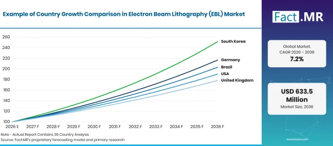
Electron Beam Lithography Ebl Market Growth Index | Source: Fact.MR
| Country | CAGR (2026–2036) |
|---|---|
| Germany | 8.1% |
| Brazil | 7.4% |
| USA | 6.7% |
| UK | 6.0% |
| Japan | 5.3% |
Source: Fact.MR analysis. Updated Nov 4, 2026
What supports Germany adoption?
8.1% CAGR, supported by a substantial semiconductor manufacturing base and investment in advanced technology.
Germany's semiconductor industry provides a strong foundation for demand for precision lithography and nanofabrication equipment. Germany Trade and Invest reported that the country's semiconductor industry generated more than EUR 17 billion in revenue in 2025, with more than one-third of European chips produced in Germany. Continued investment in semiconductor production and research can support demand for EBL systems used in device development, prototyping and specialized patterning. [5]
How is Brazil developing electron beam lithography adoption?
7.4% CAGR, driven by government initiatives to strengthen semiconductor research and production capabilities.
Brazil is working to expand its domestic semiconductor ecosystem through the Brasil Semicon programme. The Ministry of Development, Industry, Trade and Services describes the programme as an initiative to strengthen semiconductor production, research & development, innovation and chip design. These activities can support demand for specialized nanofabrication infrastructure at universities, research centres and technology-oriented companies.
Brazil's semiconductor industry is receiving policy support through the Brasil Semicon programme, established under Law No. 14,968 of September 2024 to strengthen domestic semiconductor production and expand research and innovation. The Brazilian Association of the Semiconductor Industry (ABISEMI) projected that the sector would generate approximately US$2.5 billion in revenue in 2026 [2].
What supports United States adoption?
6.7% CAGR, supported by advanced semiconductor research and demand for nanoscale device fabrication.
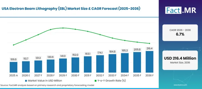
Electron Beam Lithography Ebl Market Forecast Usa | Source: Fact.MR
The United States has a well-developed semiconductor research ecosystem supported by industrial investment and national laboratories. The Semiconductor Industry Association reported that U.S.-headquartered semiconductor companies spent USD 76.8 billion on research and development in 2025. EBL systems support research into nanoscale electronic structures, photonic devices and quantum technologies. Equipment suppliers can address demand from research institutions and specialized semiconductor developers that require precise direct-write capabilities. [6]
How is the United Kingdom building adoption?
6.0% CAGR, led by semiconductor research, compound semiconductor development and advanced technology programmes.
The United Kingdom has established strengths in semiconductor research, chip design and compound semiconductor technologies. The government's 2026 semiconductor sector study identified 703 semiconductor companies in the country and highlighted the importance of research, manufacturing and materials capabilities. These activities can create opportunities for EBL systems used in prototyping, device research and specialized nanofabrication. [7]
What supports Japan adoption?
5.3% CAGR, backed by established semiconductor equipment expertise and continued investment in advanced chip technologies.
Japan's semiconductor ecosystem includes equipment manufacturers, research institutions and technology developers. The Ministry of Economy, Trade and Industry updated its semiconductor and digital industry strategy in June 2026, emphasizing the development of an integrated AI and semiconductor ecosystem. This policy direction can support investment in research and manufacturing infrastructure, including specialized lithography equipment for advanced device development. [8]
Who leads the Electron Beam Lithography Market?
Fact.MR identifies JEOL Ltd., Vistec, Raith, Crestec Corporation and NanoBeam Ltd. among the companies profiled in the electron beam lithography market.
JEOL offers electron beam lithography systems for mask and direct-write applications, including the JBX-A9, JBX-8100FS and JBX-3050MV platforms. Its portfolio addresses semiconductor research, mask and reticle fabrication and advanced patterning requirements. [9] Vistec develops, manufactures, sells and services electron beam lithography systems based on variable shaped beam technology. Its portfolio includes systems for research, prototyping and low-volume production, with capabilities for wafer and mask processing. [10]
Raith provides electron beam lithography systems for semiconductor research, photonics, quantum technologies and nanofabrication. Its portfolio includes EBPG, VOYAGER, PIONEER, E-LINE and RAITH150 platforms. [11] Crestec Corporation supplies electron beam lithography systems through its CABL product range. Its CABL-UH and CABL-AP platforms address high-resolution patterning, academic research and production applications such as distributed feedback laser structures. The company also provides electron-beam lithography foundry services. [12]
NanoBeam develops electron beam lithography equipment, including its nB5 system. The company describes the nB5 as an updated platform designed to improve performance and reduce regular service requirements. [13] Commercial competition depends on writing resolution and beam-source performance alongside stage accuracy and system throughput. Suppliers also differentiate themselves through automation capabilities and system reliability as well as application support and software functionality.
Which companies are the key providers?
Key companies include JEOL Ltd., Vistec, Raith, Crestec Corporation and NanoBeam Ltd.
- JEOL Ltd.
- Vistec
- Raith
- Crestec Corporation
- NanoBeam Ltd.
Bibliography
- [1] National Institute of Standards and Technology. (2025, April 10). Electron-beam lithography.
- [2] Associação Brasileira da Indústria de Semicondutores. (2026, May 27). Abisemi apresenta panorama do setor de semicondutores aos ministros do MDIC e MCTI.
- [3] Semiconductor Industry Association. (2026, February 6). Global annual semiconductor sales increase 25.6% to $791.7 billion in 2025.
- [4] Ministério do Desenvolvimento, Indústria, Comércio e Serviços. (2026, March 10). Programa Brasil Semicondutores (Brasil Semicon).
- [5] Germany Trade & Invest. (n.d.). Semiconductor industry in Germany.
- [6] Semiconductor Industry Association. (n.d.). Industry impact.
- [7] Department for Science, Innovation and Technology. (2026, September 2). Semiconductor sector study 2026.
- [8] Ministry of Economy, Trade and Industry. (2026, June 23). 第16回 半導体・デジタル産業戦略検討会議 [16th Semiconductor and Digital Industry Strategy Review Meeting].
- [9] JEOL Ltd. (n.d.). Electron beam lithography system.
- [10] Vistec Electron Beam GmbH. (n.d.). E-beam systems.
- [11] Raith. (n.d.). Electron beam lithography.
- [12] Crestec Corporation. (n.d.). Our business: Electron beam lithography system.
- [13] NanoBeam Ltd. (n.d.). Welcome to NanoBeam.
This Report Answers
- The report describes how electron beam lithography systems are used in semiconductor research and nanoscale pattern fabrication.
- Type analysis compares thermionic sources and field electron emission sources.
- Application analysis evaluates electronic, research institute and industrial applications alongside other uses.
- Country analysis discusses Germany, Brazil, USA, UK and Japan in relation to semiconductor investment and research infrastructure.
- The competitive overview profiles five companies involved in electron beam lithography equipment development and supply.
What does the Electron Beam Lithography Market cover?
The market covers electron beam lithography systems and associated equipment that use focused electron beams to create high-resolution patterns on suitable substrates. These systems are used in semiconductor research, nanofabrication, photonics, quantum device development and specialized industrial applications. Market coverage includes systems using thermionic and field electron emission sources, along with equipment designed for electronic, research and industrial applications.
What is included in the scope?
The analysis includes dedicated electron beam lithography systems, direct-write equipment and relevant system configurations used for nanoscale pattern fabrication.
It covers equipment differentiated by electron source technology and application area. Systems used in academic research, semiconductor prototyping, mask and reticle writing, photonic device development and specialized industrial patterning are considered within the defined market boundary.
What is excluded from the scope?
The analysis excludes conventional optical lithography equipment, extreme ultraviolet lithography systems and other patterning technologies that do not use a focused electron beam for direct writing.
Standalone scanning electron microscopes without lithography functionality are excluded. Electron microscopy equipment, general-purpose semiconductor manufacturing tools, resist materials, patterning chemicals and unrelated nanofabrication services are not counted as EBL equipment revenue unless explicitly included in a qualifying system or service category.
How Was the Analysis Built?
The analysis draws on 120+ sources, 35+ company portfolios, 25+ countries and more than 20 industry interviews.
- Primary Research: Primary research includes discussions with electron-beam equipment manufacturers, semiconductor equipment distributors, research institutions, nanofabrication laboratories, industrial users and subject-matter experts. These conversations examine system purchasing priorities, resolution requirements, operating costs, equipment utilization, application development and factors influencing adoption.
- Desk Research: Desk research covers government semiconductor strategies, research institution publications, company product portfolios, equipment specifications, technical studies, industry association data and public investment announcements. Every source used in the analysis is documented in the bibliography.
- Market Sizing and Forecasting: Market estimates combine historical performance, equipment demand indicators, pricing and shipment trends, system installations, segment shares, company participation, country-level growth and barriers to market expansion.
- Data Validation and Update Cycle: Findings are validated by comparing primary interviews with public data, product specifications, company activity, research infrastructure investments and industry developments. Regular updates review new system launches, product upgrades, customer installations, partnerships and changes in commercial adoption.
Segmentation
What is the report’s scope and coverage?
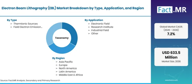
Electron Beam Lithography Ebl Market Taxonomy | Source: Fact.MR
| Attribute | Details |
|---|---|
| Quantitative Units | USD million in 2026 to USD million by 2036, at CAGR |
| Market Definition | The Electron Beam Lithography (EBL) Market comprises specialized systems that use focused electron beams to directly write high-resolution patterns onto electron-sensitive resist-coated substrates. These systems enable nanoscale fabrication for semiconductor devices and photomasks as well as photonics and advanced research applications. |
| Type | Thermionic Sources; Field Electron Emission Sources |
| Application | Electronic Field; Research Institute; Industrial Field; Other |
| Regions Covered | North America; Latin America; Western Europe; Eastern Europe; East Asia; South Asia & Pacific; Middle East & Africa |
| Countries Covered | Germany; Brazil; USA; UK; Japan |
| Companies Profiled | JEOL Ltd.; Vistec; Raith; Crestec Corporation; NanoBeam Ltd. |
| Forecast Period | 2026 to 2036 |
| Approach | Market segmentation and scenario-based analysis supported by equipment portfolios, technology specifications, semiconductor industry statistics and research infrastructure developments |
Source: Fact.MR analysis. Updated Nov 4, 2026
How is the market segmented?
-
By Type
- Thermionic Sources
- Field Electron Emission Sources
-
By Application
- Electronic Field
- Research Institute
- Industrial Field
- Other
-
By Region
- North America
- Latin America
- Western Europe
- Eastern Europe
- East Asia
- South Asia & Pacific
- Middle East & Africa
Frequently Asked Questions
How big is the electron beam lithography market in 2026?
What is the CAGR from 2026 to 2036?
Which type has the largest market share?
Which application leads the market?
Which country is expected to grow fastest?
Which companies are covered in the report?
Who worked on this report


Preview the report firsthand - request a free sample
Free SampleGet the brochure for pricing and purchase details
Download PDF