- Market Value (2025): USD 1.7 Bn
- Estimated Value (2026): USD 1.9 Bn
- Forecast Value (2036): USD 5.2 Bn
- CAGR (2026-2036): 10.7%
What is the Heterogeneous Chip Integration Tools Market forecast to be worth by 2036?
USD 1.9 billion in 2026 to USD 5.2 billion by 2036 at a 10.7% CAGR.
- The Heterogeneous Chip Integration Tools Market reached USD 1.7 billion in 2025.
- Demand is expected to increase from USD 1.9 billion in 2026 to USD 5.2 billion by 2036.
- The market is forecast to record 10.7% CAGR from 2026 to 2036 as foundries, IDMs. Advanced packaging operations expand multi-die integration flows.
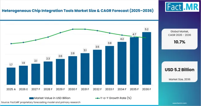
Heterogeneous Chip Integration Tools Market Value Analysis | Source: Fact.MR
What are the defining numbers behind Heterogeneous Chip Integration Tools Market growth?
An absolute opportunity of USD 3.3 billion is expected between 2026 and 2036.
- Demand Drivers in the Market
- Advanced packaging engineering teams need tighter overlay and surface control as hybrid bonding reduces allowable alignment and planarity margins at finer interconnect pitch. In January 2025, the U.S. Department of Commerce finalized USD 1.4 billion in CHIPS advanced-packaging awards, including funding for pilot-line and substrate capabilities.
- Foundries need integrated process flows for 2.5D and 3D designs as chiplets move functions from a single die into coordinated multi-die packages. The package becomes part of the electrical and mechanical design, so tool teams must control alignment and surface condition across connected steps.
- Memory makers need wafer preparation and bonding tools that handle stacked structures while protecting yield through thinning and cleaning. Alignment and interconnect formation add further control needs once dies move into high-density stacks.
- Inspection teams need packaging-specific metrology because bonded wafers and larger packages introduce warpage and buried interfaces. Mixed materials can change how structures respond during handling or measurement.
- Key Segments Analyzed
- By Tool Class: Hybrid bonding is expected to hold 35.0% share in 2026. Direct copper and dielectric bonding supports dense die-to-wafer and wafer-to-wafer integration.
- By Integration: 2.5D interposer is expected to hold 31.0% share in 2026 owing to established use in high-performance logic and memory integration.
- By Wafer Size: 200 mm is expected to capture 36.0% share in 2026 as heterogeneous integration spans mature specialty devices alongside leading-edge logic and memory.
- By Process Stage: Wafer prep is expected to hold 32.0% share in 2026 since cleaning, planarization, thinning, and surface conditioning determine downstream bonding yield.
- Analyst Opinion at Fact.MR
- Shambhu Nath Jha, Principal Consultant at Fact.MR, states, “Heterogeneous integration makes packaging equipment behave more like front-end process equipment. Yield increasingly depends on how well surface preparation, bonding accuracy, and metrology operate as one flow. Suppliers are expected to gain relevance where they connect precise process modules with usable process-control data and high-volume manufacturing support.”
- Strategic Implications
- Equipment suppliers should connect bonding and metrology data so process engineers can trace overlay drift before package-level yield loss occurs. In September 2025, EV Group introduced the EVG40 D2W platform with 100% die overlay measurement on 300 mm wafers and up to 15X higher throughput than its previous benchmark system.
- Foundry engineering teams should qualify wafer-preparation steps together with the target bond process. Surface chemistry and planarity directly affect interface quality.
- OSAT operators should build warpage and handling controls into tool selection when they move from standard packages toward larger interposers and multi-die assemblies.
Japan is expected to post 11.5% CAGR through 2036, supported by public chip investment and advanced-node capacity programs. The USA is expected to record 11.2%, while Germany is estimated at 10.9%. France is forecast to reach 10.6%, and the UK is expected to advance at 10.1% as chip infrastructure and R&D programs expand.
How does the Heterogeneous Chip Integration Tools Market break down by segment?
Hybrid bonding leads Tool Class at 35.0%; 200 mm leads Wafer Size at 36.0%.
Which Tool Class dominates?
Hybrid bonding is expected to hold 35.0% share in 2026.
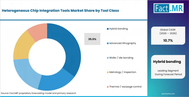
Heterogeneous Chip Integration Tools Market Analysis By Tool Class | Source: Fact.MR
Hybrid bonding is expected to lead as chiplet packages move toward denser die connections than standard assembly supports. The process places more weight on surface flatness and cleanliness because small interface errors can affect bond quality. Overlay control becomes equally important when dies are placed at finer pitch. Equipment suppliers so need to connect preparation and bonding with process-control feedback.
What leads the Integration segment?
2.5D interposer leads with 31.0% share in 2026.
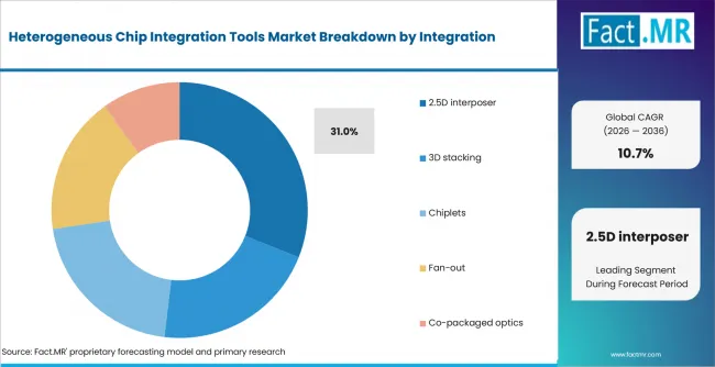
Heterogeneous Chip Integration Tools Market Analysis By Integration | Source: Fact.MR
2.5D interposers are expected to lead because they place logic and high-bandwidth memory close together while allowing each die to use a suitable process node. The interposer adds routing and alignment work outside the individual dies. That structure increases tool use across lithography and bonding. Inspection becomes more valuable because defects can appear at the interposer surface or at the die interface. Suppliers with packaging-specific process control are expected to benefit when makers move more system functions into the package and require repeatable multi-die assembly.
How does Wafer Size shape demand?
200 mm accounts for 36.0% share in 2026.
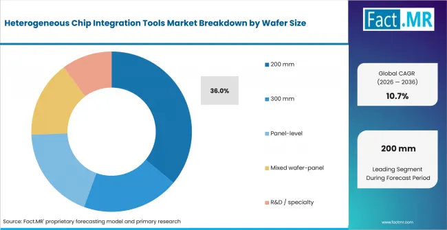
Heterogeneous Chip Integration Tools Market Analysis By Wafer Size | Source: Fact.MR
The 200 mm segment is expected to retain the largest share. Heterogeneous integration serves specialty devices and photonics alongside leading-edge logic. Many established lines already use 200 mm equipment for device types that enter multi-die packages. These lines can add bonding or metrology capability without changing every upstream process. The format so remains relevant for work and specialty production. Tool selection is expected to reflect the installed wafer base and the target integration flow. 300 mm systems gain importance where high-volume logic and memory packaging requires larger-scale processing.
What supports Wafer prep within Process Stage?
Wafer prep captures 32.0% share in 2026.
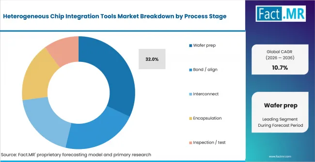
Heterogeneous Chip Integration Tools Market Analysis By Process Stage | Source: Fact.MR
Wafer preparation is expected to lead because bonding yield depends on flatness and controlled surface topography. Cleaning removes contamination before surfaces reach the bond step. CMP supports the planarity needed for tighter interfaces, while activation prepares surfaces for reliable joining. Small variation at this stage can carry into alignment and bonding performance later in the flow. Process engineers so evaluate preparation steps together with the target bonding method. Suppliers that connect preparation with measurable surface-control data are expected to support faster testing when makers introduce new chiplet or stacked-die designs.
What is accelerating Heterogeneous Chip Integration Tools Market adoption, and what is holding it back?
Chiplet scaling drives adoption; process-control complexity restrains it.
Drivers Impact Analysis
| DRIVER | (~) % IMPACT ON CAGR | GEOGRAPHIC RELEVANCE | IMPACT TIMELINE |
|---|---|---|---|
| Hybrid bonding adoption for fine-pitch chiplet stacks | +1.8% | North America, Europe, East Asia | Short term (<= 2 years) |
| HBM and AI package integration | +1.5% | North America, East Asia | Medium term (2-4 years) |
| Advanced packaging capacity investment | +1.2% | North America, Europe, East Asia | Medium term (2-4 years) |
| Higher inspection and metrology intensity | +0.9% | Global | Long term (>= 4 years) |
Opportunity Impact Analysis
| OPPORTUNITY | (~) % IMPACT ON CAGR | GEOGRAPHIC RELEVANCE | IMPACT TIMELINE |
|---|---|---|---|
| Integrated die-to-wafer hybrid bonding cells | +1.3% | North America, East Asia | Medium term (2-4 years) |
| 300 mm packaging metrology and inspection | +1.0% | Global | Short term (<= 2 years) |
| Co-packaged optics integration tools | +0.8% | North America, Europe, East Asia | Long term (>= 4 years) |
Restraints Impact Analysis
| RESTRAINT | (~) % IMPACT ON CAGR | GEOGRAPHIC RELEVANCE | IMPACT TIMELINE |
|---|---|---|---|
| High tool qualification cost | -0.7% | Global | Short term (<= 2 years) |
| Yield sensitivity across bonded interfaces | -0.6% | Global | Medium term (2-4 years) |
| Skills and process-integration constraints | -0.4% | North America, Europe, East Asia | Long term (>= 4 years) |
Which countries are scaling the Heterogeneous Chip Integration Tools Market through 2036?
- Japan is expected to record 11.5% CAGR, the upper end of the supplied country range.
- The USA is projected at 11.2% CAGR as advanced packaging and domestic chip investment expand.
- Germany is estimated at 10.9% CAGR through chip-fab investment and European microelectronics programs.
- France is forecast to post 10.6% CAGR as public chip funding and electronics production activity support equipment demand.
- The UK is expected to reach 10.1% CAGR through chip infrastructure, AI hardware, and compound-chip investment.
The country comparison spans 1.4 percentage points. Entry conditions differ by wafer-fab scale, packaging specialization, public investment, energy costs, and access to engineering talent. These differences are expected to shape the tool mix in each country.
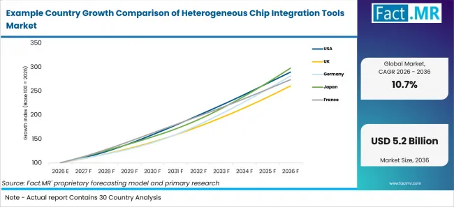
Example Country Growth Comparison Of Heterogeneous Chip Integration Tools Market | Source: Fact.MR
| Country | CAGR (2026-2036) |
|---|---|
| Japan | 11.5% |
| United States | 11.2% |
| Germany | 10.9% |
| France | 10.6% |
| United Kingdom | 10.1% |
What supports USA adoption?
11.2% CAGR, supported by advanced-packaging research infrastructure and domestic chip production.
U.S. packaging teams are expected to place greater weight on pilot-line access and process transfer as multi-die production expands. In January 2025, the U.S. Department of Commerce awarded USD 285 million to establish the SMART USA institute, with more than USD 1 billion in combined investment focused on digital twins for chip production, advanced packaging, assembly, and test. That infrastructure is expected to support testing work for bonding, metrology, and process-control tools.
How is the United Kingdom scaling demand?
10.1% CAGR, backed by chip infrastructure and AI hardware programs.
The United Kingdom is expected to build tool demand around design-led chip activity and new hardware programs. In June 2026, the Department for Science, Innovation and Technology announced an AI Hardware Plan backed by over GBP 1.1 billion in targeted public and private investment, including GBP 750 million for a national AI supercomputer and funding for next-generation AI chips. The program is expected to strengthen the route from chip design into physical hardware work, creating more demand for packaging tools used in chiplet and heterogeneous integration flows.
What is supporting Germany’s adoption?
10.9% CAGR, led by chip-fab investment and European microelectronics programs.
Germany is expected to link heterogeneous-integration equipment demand with fab investment and its established automotive and industrial electronics base. In February 2025, Germany’s Federal Ministry for Economic Affairs and Climate Action reported that Infineon planned to invest around EUR 3.4 billion at its Dresden site. Additional production capacity is expected to raise demand for process equipment and engineering support around specialty chips, wafer preparation, inspection, and advanced packaging.
How does Japan perform?
11.5% CAGR, driven by next-generation chip investment and advanced production programs.
Japan is expected to retain a close link between precision equipment expertise and next-generation chip production. In November 2025, the Ministry of Economy, Trade and Industry selected Rapidus for support and stated that JPY 100 billion from the fiscal 2025 budget was intended for investment through the Information-technology Promotion Agency. That program is expected to support advanced process work where bonding accuracy and metrology become central to production readiness.
What supports France adoption?
10.6% CAGR, reinforced by public chip funding and electronics production activity.
France is expected to develop demand through chip investment that connects research capability with industrial electronics production. In May 2026, France announced a EUR 550 million contribution to the European IPCEI on Advanced Semiconductor Technologies to support semiconductor research and industrialization for applications including AI and data centers. The funding is expected to support projects that expand local chip capability and create a wider base for packaging, inspection, bonding, and wafer-processing tools.
Who leads the Heterogeneous Chip Integration Tools Market?
Applied Materials spans multiple advanced-packaging process steps, including deposition, CMP, surface preparation, and eBeam process control. Its portfolio supports several stages that determine wafer and surface conditions before and during advanced packaging integration. Lam Research supplies etch technology for heterogeneous-integration flows, including processes involving high-bow wafers bonded to glass carriers, where wafer handling, profile control, and process stability are important.
KLA provides inspection and metrology systems for advanced wafer-level packaging that help manufacturers detect, resolve, and monitor process excursions. ASM International supports advanced packaging through technologies including ALD, PECVD, surface preparation, and related materials-engineering processes. Together, these suppliers address multiple process stages across advanced packaging rather than a single assembly operation.
EV Group supplies wafer-bonding technology, die-to-wafer preparation and activation equipment, lithography systems, and overlay metrology. BESI supplies die-attach, flip-chip, thermocompression-bonding, and hybrid-bonding equipment for advanced packaging applications. Their portfolios extend advanced-packaging equipment coverage from surface preparation and bonding to die placement and process measurement.
Equipment differentiation across these suppliers includes placement and overlay accuracy, process repeatability, throughput, process-control capability, equipment integration, and support for high-volume manufacturing. Service and installed-base support can also influence production deployment because advanced-packaging flows rely on coordinated performance across multiple processing and assembly steps.
Which companies are the key providers?
Key companies include Applied Materials, Lam Research, KLA, ASM International, EV Group, and BESI.
- Applied Materials
- Lam Research
- KLA
- ASM International
- EV Group
- BESI
Bibliography
- EV Group. (2025, September 8). EV Group achieves breakthrough in hybrid bonding overlay control for chiplet integration.
- Lam Blog Staff. (2025, October 2). Lam researchers spotlight etch breakthrough for advanced packaging. Lam Research.
- Applied Materials, Inc. (2026, June 25). Applied Materials introduces new systems to accelerate DRAM and advanced packaging for AI chips.
- Ministère de l’Économie, des Finances et de la Souveraineté industrielle, énergétique et numérique. (2026, May 26). Souveraineté technologique : la France investit 1 milliard d’euros supplémentaire dans la stratégie nationale quantique et 550 M€ dans les semi-conducteurs.
- Ministry of Economy, Trade and Industry. (2025, November 21). Press conference by Minister Akazawa (excerpt).
- Federal Ministry for Economic Affairs and Climate Action. (2025, February 20). Europäische Kommission genehmigt weiteres deutsches Chips-Act-Projekt: Infineon baut seine Chip-Produktion in Dresden aus [European Commission approves another German Chips Act project: Infineon expands chip production in Dresden].
- Department for Science, Innovation and Technology. (2026, June 8). A decisive shift to power British AI: New £1.1 billion plan to back chip firms, boost computing power and skills for the AI revolution.
- U.S. Department of Commerce. (2025, January 3). Biden-Harris Administration awards Semiconductor Research Corporation Manufacturing Consortium Corporation $285M for new CHIPS Manufacturing USA Institute for Digital Twins, headquartered in North Carolina.
- U.S. Department of Commerce. (2025, January 16). U.S. Department of Commerce announces $1.4 billion in final awards to support the next generation of U.S. semiconductor advanced packaging.
This Report Answers
- The report explains where heterogeneous chip integration tools are used across Tool Class and Integration. It also covers Wafer Size and Process Stage, together with regional deployment.
- Segment analysis identifies the leading subsegments and the operational reasons semiconductor manufacturers prioritize hybrid bonding, 2.5D interposers, 200 mm processing, and wafer preparation.
- Country analysis examines Japan, the United States, Germany, France, and the United Kingdom. It also considers semiconductor investment, advanced-packaging infrastructure, chip-fab expansion, and public technology programs supporting equipment demand.
- Competitive analysis reviews Applied Materials, Lam Research, KLA, ASM International, EV Group, and BESI. It covers wafer preparation, deposition, etch, bonding, inspection, metrology, die placement, and process-control capabilities.
- Application analysis assesses how bonding accuracy, surface preparation, process repeatability, overlay control, inspection, metrology, and wafer handling influence tool selection. It also considers 2.5D, 3D, chiplet, fan-out, and co-packaged optics integration flows.
What does the Heterogeneous Chip Integration Tools Market cover?
Bonding, lithography, metrology, wafer-preparation, interconnect, and package-control tools used for heterogeneous chip integration.
The market covers tools used to prepare wafers or dies, pattern package layers, align components, form bonds and inspect multi-die structures. It spans hybrid bonding, lithography, metrology and warpage control used in heterogeneous integration.
What is included in the scope?
Heterogeneous integration tools used across wafer, die, interposer, and advanced-packaging process flows.
Coverage includes hybrid and wafer or die bonding, packaging lithography, metrology, wafer preparation, interconnect, and warpage control. It spans 2.5D, 3D, chiplet, fan-out, and co-packaged optics flows across 200 mm, 300 mm, and panel formats. Related coverage includes 3D semiconductor packaging, advanced substrate packages, queue-time hybrid bonders, and HBM silicon interposers and substrates.
What is excluded from the scope?
Scope boundaries separate integration equipment from standalone chip-design software, raw chip materials, and general front-end tools.
Scope boundaries cover tool used directly in heterogeneous integration. Standalone EDA software, chip devices, raw materials, and substrates are treated as adjacent categories. Front-end tools enter scope when the vendor identifies a direct advanced-packaging or heterogeneous-integration use.
How Was the Analysis Built?
The analysis draws on 120+ sources, 35+ company portfolios, 25+ countries, and more than 20 industry interviews.
- Primary Research: Primary research includes discussions with manufacturers, service providers, technology developers, distributors, end users, and subject-matter experts. These conversations examine purchasing priorities, product adoption, operational challenges, approval requirements, competitive positioning, and the factors that influence wider market acceptance.
- Desk Research: Desk research covers government statistics, regulatory publications, company filings, trade data, technical studies, industry associations, standards, public policy, and other authoritative sources. Every source used in the analysis is documented in the bibliography.
- Market Sizing and Forecasting: Market estimates combine historical performance, demand indicators, pricing and volume trends, segment shares, company participation, country-level growth, adoption patterns, investment activity, and barriers to market expansion.
- Data Validation and Update Cycle: Findings are validated by comparing primary interviews with public data, company activity, regulatory changes, trade patterns, and industry developments. Regular updates review new product launches, capacity changes, partnerships, approvals, and shifts in commercial adoption.
What is the report’s scope and coverage?
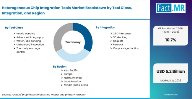
Heterogeneous Chip Integration Tools Market Breakdown By Tool Class, Integration, And Region | Source: Fact.MR
| Attribute | Details |
|---|---|
| Quantitative Units | USD billion |
| Market Definition | Equipment and process tools used to fabricate, align, bond, inspect, and prepare wafers or dies for heterogeneous chip integration and advanced multi-die packaging. |
| Tool Class | Hybrid bonding; Advanced lithography; Wafer and die bonding; Metrology and inspection; Thermal and warpage control |
| Integration | 2.5D interposer; 3D stacking; Chiplets; Fan-out; Co-packaged optics |
| Wafer Size | 200 mm; 300 mm; Panel-level; Mixed wafer-panel; R&D and specialty |
| Process Stage | Wafer prep; Bond and align; Interconnect; Encapsulation; Inspection and test |
| Regions Covered | North America; Latin America; Western Europe; Eastern Europe; East Asia; South Asia and Pacific; Middle East and Africa |
| Countries Covered | United States; United Kingdom; Germany; Japan; France |
| Key Companies Profiled | Applied Materials; Lam Research; KLA; ASM International; EV Group; BESI |
| Forecast Period | 2026 to 2036 |
| Approach | Hybrid top-down and bottom-up approach using equipment portfolio mapping, packaging process intensity, wafer and die integration flows, country manufacturing programs, and provider validation. |
How is the market segmented?
-
By Tool Class:
- Hybrid bonding
- Advanced lithography
- Wafer and die bonding
- Metrology and inspection
- Thermal and warpage control
-
By Integration:
- 2.5D interposer
- 3D stacking
- Chiplets
- Fan-out
- Co-packaged optics
-
By Wafer Size:
- 200 mm
- 300 mm
- Panel-level
- Mixed wafer-panel
- R&D and specialty
-
By Process Stage:
- Wafer prep
- Bond and align
- Interconnect
- Encapsulation
- Inspection and test
-
By Region:
- North America
- Latin America
- Western Europe
- Eastern Europe
- East Asia
- South Asia and Pacific
- Middle East and Africa