- Market Value (2025): USD 2.2 Bn
- Estimated Value (2026): USD 2.6 Bn
- Forecast Value (2036): USD 12.3 Bn
- CAGR (2026-2036): 16.9%
What is the Heterogeneous IC Suites Market forecast to be worth by 2036?
USD 2.6 Billion in 2026 to USD 12.3 Billion by 2036, at 16.9% CAGR.
- The Heterogeneous IC Suites Market reached USD 2.2 Billion in 2025.
- Demand is projected to increase from USD 2.6 Billion in 2026 to USD 12.3 Billion by 2036.
- The market is forecast to record 16.9% CAGR from 2026 to 2036 as chip architects and package teams align multi-die design with manufacturable integration flows.
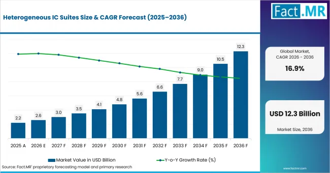
Heterogeneous Ic Suites Value Analysis | Source: Fact.MR
What are the defining numbers behind Heterogeneous IC Suites Market growth?
USD 9.7 Billion absolute opportunity by 2036, led by chiplet architecture, 2.5D interposer and AI / HPC.
- Demand Drivers in the Market
- Chip architects need architecture planning that links compute partitioning with die-to-die interfaces. The UCIe Consortium released the 3.0 specification in August 2025 with 64 GT/s performance.
- Package engineering teams need interposer-aware layout views due to tighter signal routing and high-bandwidth memory placement inside AI accelerators.
- EDA platform teams need shared databases for die, substrate and thermal checks, supported by certification activity across foundry ecosystems.
- Design verification teams need signoff workflows that connect electrical and mechanical behavior before the design enters package qualification.
- Key Segments Analyzed
- By Suite Module: Chiplet architecture is projected to hold 24.0% share in 2026 since multi-die planning starts with partitioning and interface choices.
- By Integration: 2.5D interposer is anticipated to account for 31.0% share in 2026 owing to its established role in logic and HBM placement.
- By End Market: AI / HPC is estimated to capture 35.0% share in 2026 because accelerator designs require bandwidth, cooling and package-aware verification.
- By Design Automation: Rule-based EDA is forecast to represent 37.0% share in 2026 reflecting the continued use of constraints and repeatable checks.
- Analyst Opinion at Fact.MR
- Shambhu Nath Jha, Principal Consultant at Fact.MR, states, “The design boundary for heterogeneous ICs now runs across chiplet, package and board assumptions. Demand is expected to move toward suites that show timing, thermal and power tradeoffs before layout choices become fixed. Suppliers need certified foundry flows, interconnect checks and usable thermal evidence in one workflow.”
- Strategic Implications
- EDA vendors should connect architecture planning with package layout so engineering teams avoid rebuilding constraints across separate tools.
- Foundry ecosystem teams should publish certified multi-die reference flows. Cadence reported in June 2025 that a Samsung SF2 high-speed CPU flow with Voltus InsightAI reached 80-90% resolution of IR-drop violations.
- System companies should require power and thermal evidence before approving chiplet partitioning for AI accelerator programs.
- Packaging partners should align interposer, bridge and substrate rules with design-suite data models used by customer engineering teams.
Taiwan is projected to record 17.5% CAGR through 2036, supported by semiconductor output and packaging capacity. Japan is expected to post 17.2% CAGR due to Rapidus-backed logic programs. The USA is anticipated to advance at 16.8% CAGR with CHIPS R&D support. South Korea is forecast to record 16.5% CAGR, led by HBM and memory-package co-design. The UK is estimated to post 12.5% CAGR, shaped by chip-design clusters and AI hardware policy.
How does the Heterogeneous IC Suites Market break down by segment?
Chiplet architecture leads at 24.0%; 2.5D interposer leads at 31.0%.
Which Suite Module dominates?
Chiplet architecture holds 24.0% share in 2026.
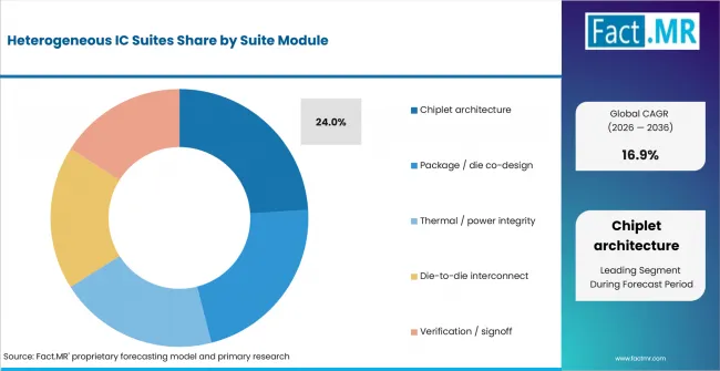
Heterogeneous Ic Suites Analysis By Suite Module | Source: Fact.MR
Chiplet architecture leads because system companies split compute, memory and I/O across specialized dies. Architecture tools test partitioning before package rules become fixed. UCIe 3.0 gives design teams a higher-speed interconnect target for multi-chip systems.
What leads the Integration segment?
2.5D interposer leads with 31.0% share in 2026.
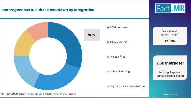
Heterogeneous Ic Suites Analysis By Integration | Source: Fact.MR
2.5D interposer remains practical for many AI and HPC packages because it places logic dies and HBM on a shared routing platform. Cadence stated in April 2025 that its collaboration with TSMC expanded support for TSMC 3DFabric and included TSMC 9000-certified HBM3E IP alongside UCIe 16G solutions on TSMC N3P.
How does End Market shape demand?
AI / HPC holds 35.0% share in 2026.
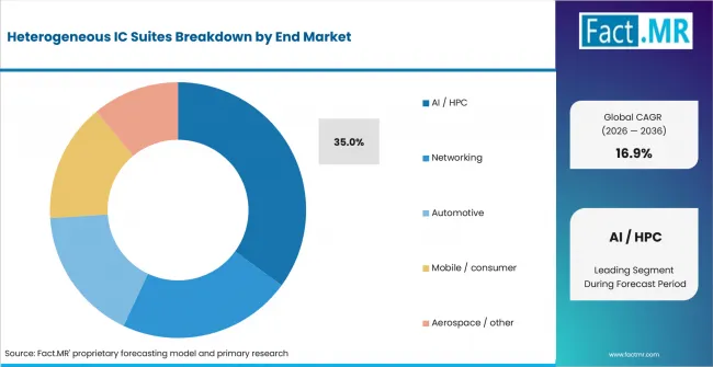
Heterogeneous Ic Suites Analysis By End Market | Source: Fact.MR
AI / HPC leads because accelerator designs force more decisions into the package stage. Bandwidth, power delivery and heat flow have to be checked together. The U.S. Department of Commerce finalized USD 1.4 Billion in CHIPS advanced packaging awards in January 2025.
What supports Rule-based EDA within Design Automation?
Rule-based EDA accounts for 37.0% share in 2026.
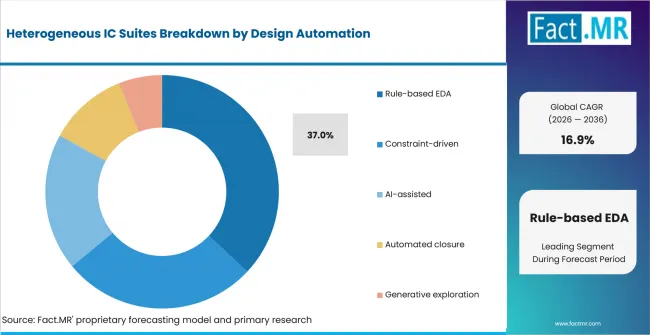
Heterogeneous Ic Suites Analysis By Design Automation | Source: Fact.MR
Rule-based EDA holds the larger automation share because heterogeneous packages still depend on explicit electrical, spacing and thermal constraints. Synopsys and Intel Foundry announced an EMIB-T reference flow in April 2025 for 2.5D and 3D multi-die designs.
What is accelerating Heterogeneous IC Suites Market adoption, and what is holding it back?
Demand is expected to rise through chiplet partitioning and interposer co-design. Growth is constrained by tool integration cost and qualification risk.
Drivers Impact Analysis
| DRIVER | (~) % IMPACT ON CAGR | GEOGRAPHIC RELEVANCE | IMPACT TIMELINE |
|---|---|---|---|
| Chiplet partitioning for AI and HPC systems | +2.0% | USA, Taiwan, Japan | Short term (<= 2 years) |
| 2.5D interposer and HBM package co-design | +1.6% | Taiwan, South Korea, Japan | Medium term (2-4 years) |
| Foundry-certified multi-die reference flows | +1.1% | Global | Medium term (2-4 years) |
| Die-to-die interface standardization | +0.8% | USA, Japan, UK | Long term (>= 4 years) |
Opportunity Impact Analysis
| OPPORTUNITY | (~) % IMPACT ON CAGR | GEOGRAPHIC RELEVANCE | IMPACT TIMELINE |
|---|---|---|---|
| AI-assisted exploration inside certified flows | +1.3% | USA, Taiwan, UK | Short term (<= 2 years) |
| Thermal and power-integrity closure for stacked designs | +1.0% | Taiwan, South Korea, Japan | Medium term (2-4 years) |
| Interconnect validation across UCIe and custom links | +0.9% | Global | Long term (>= 4 years) |
Restraints Impact Analysis
| RESTRAINT | (~) % IMPACT ON CAGR | GEOGRAPHIC RELEVANCE | IMPACT TIMELINE |
|---|---|---|---|
| Toolchain fragmentation across die and package teams | -0.8% | Global | Short term (<= 2 years) |
| Qualification burden for advanced package flows | -0.6% | Taiwan, USA, Japan | Medium term (2-4 years) |
| Limited specialist engineers for multiphysics signoff | -0.4% | UK, Japan, South Korea | Long term (>= 4 years) |
Which countries are scaling the Heterogeneous IC Suites Market through 2036?
- The country comparison spans 5.0 percentage points and forms three practical growth bands across the forecast period.
- Taiwan remains 0.3 percentage point above Japan as semiconductor output and AI-server cycles support faster suite spending.
- Japan remains 0.4 percentage point above the USA due to 2 nm logic work and chiplet package research.
- The USA remains 0.3 percentage point above South Korea with CHIPS advanced packaging and digital-twin programs.
- South Korea remains 4.0 percentage points above the UK, supported by HBM and memory-centric package co-design.
- The UK closes the displayed range through semiconductor design strengths, heterogeneous integration research and AI hardware policy support.
Comparable CAGRs create different entry conditions due to compute availability, advanced packaging policy, HBM exposure and enterprise AI-silicon maturity. Full report coverage includes North America, Latin America, Western Europe, Eastern Europe, East Asia, South Asia & Pacific, Middle East & Africa.
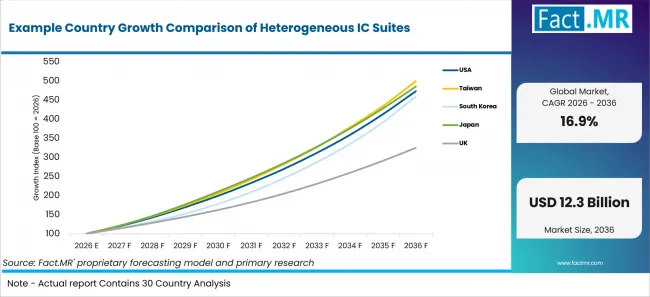
Example Country Growth Comparison Of Heterogeneous Ic Suites | Source: Fact.MR
| Country | CAGR |
|---|---|
| Taiwan | 17.5% |
| Japan | 17.2% |
| USA | 16.8% |
| South Korea | 16.5% |
| UK | 12.5% |
What supports Taiwan adoption?
17.5% CAGR, supported by AI semiconductor output and advanced packaging capability.
Taiwan’s IC design and package engineering base gives suite providers a close route into multi-die projects. DGBAS reported in February 2026 that Taiwan’s manufacturing sector grew 24.68% year over year in Q4 2025, mainly due to output expansion in semiconductors, computers, electronics and optical products. Local foundry and OSAT workflows place architecture decisions near interposer and substrate constraints. Suite adoption is expected to move faster where chiplet partitioning and package verification happen inside the same customer program.
How does Japan perform?
17.2% CAGR, led by advanced logic programs and chiplet package development.
Japan’s advanced logic programs keep heterogeneous integration near national technology planning. METI said in November 2025 that it planned to invest JPY 100 Billion in Rapidus through the Information-Technology Promotion Agency for fiscal 2025. The program reinforces demand for tools that link die planning with package behavior before qualification. Suite vendors with Japanese-language support and reliability evidence gain clearer entry into advanced logic and AI hardware projects.
What supports USA adoption?
16.8% CAGR, backed by CHIPS packaging R&D and digital-twin infrastructure.
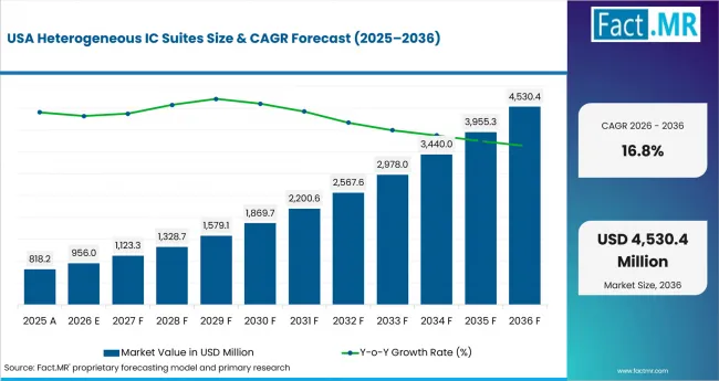
Heterogeneous Ic Suites Country Value Analysis | Source: Fact.MR
U.S. semiconductor design teams are pairing chiplet architecture with federally backed packaging research. The U.S. Department of Commerce awarded USD 285 Million in January 2025 to establish the SMART USA digital-twin semiconductor institute. Federal support connects design, manufacturing and advanced packaging data earlier in the workflow. Large AI accelerator developers are expected to favor suites that keep electrical and thermal checks traceable across design reviews.
How is South Korea scaling demand?
16.5% CAGR, supported by memory leadership and advanced packaging support.
South Korea’s demand is tied to memory, HBM and foundry programs that need package-aware design. MOTIE announced in June 2025 that semiconductor exports reached USD 13.8 Billion in May 2025. HBM placement makes thermal, signal and power checks more visible during package planning. Suite providers gain where they support memory-centric workflows and align output with manufacturing validation.
What supports the United Kingdom’s growth?
12.5% CAGR, shaped by chip design strengths and heterogeneous integration research.
UK growth comes from a design-led semiconductor base and policy support for AI hardware. The UK government's Semiconductor Sector Study 2026 identifies 703 UK semiconductor companies, comprising 295 dedicated and 408 diversified companies. Those design clusters create demand for suites that connect architecture choices with verification evidence. Tool adoption is expected to concentrate first among AI hardware and compound semiconductor firms that need package-aware collaboration.
Who leads the Heterogeneous IC Suites Market?
Cadence and Synopsys provide comprehensive design environments for multi-die and 3D-IC workflows, while Siemens EDA has expanded its 2.5D and 3D IC coverage. Cadence’s 2025 collaboration with TSMC included certified advanced-node design flows, expanded TSMC 3DFabric support and multiphysics analysis across timing, power integrity and thermal domains. Synopsys completed its acquisition of Ansys in July 2025, combining silicon design and IP capabilities with simulation and analysis technologies.
Keysight Technologies supports chiplet and 3DIC interconnect design, simulation and validation. Zuken supports heterogeneous integration through IC-package design, multi-die workflows and chiplet co-design and joined TSMC’s Open Innovation Platform EDA Alliance in July 2026. Across these suppliers, portfolios emphasize foundry-certified or validated design flows, die-to-die interconnect support, multiphysics and signoff capabilities, and integrated workflows intended to reduce design complexity and iteration risk in multi-die programs.
Which companies are the key providers?
Key companies include Cadence Design Systems, Inc.; Synopsys, Inc. (including Ansys); Siemens EDA; Keysight Technologies; and Zuken Inc.
- Cadence Design Systems, Inc.
- Synopsys, Inc. (including Ansys)
- Siemens EDA
- Keysight Technologies
- Zuken Inc.
Bibliography
- Cadence Design Systems, Inc. (2025, June 16). Cadence accelerates SoC, 3D-IC and chiplet design for AI data centers, automotive and connectivity in collaboration with Samsung Foundry.
- Cadence Design Systems, Inc. (2025, April 24). Cadence and TSMC advance AI and 3D-IC chip design with certified design solutions for TSMC’s A16 and N2P process technologies.
- Department for Business, Innovation, Science and Trade, & Department for Science, Innovation and Technology. (2026, June 8). Semiconductor sector study 2026.
- Directorate General of Budget, Accounting and Statistics, Executive Yuan, R.O.C. (2026, February 13). GDP: Preliminary estimate for 2025Q4, and outlook for 2026.
- Keysight Technologies, Inc. (2026, February 17). Keysight unveils 3D Interconnect Designer for chiplet and 3DIC advanced package designs.
- Ministry of Economy, Trade and Industry. (2025, November 21). Press conference by Minister Akazawa (Excerpt).
- Ministry of Trade, Industry and Energy. (2025, June 2). Korea’s exports decline 1.3% in May.
- Zuken Inc. (2026, July 8). Zuken joins TSMC’s Open Innovation Platform® EDA Alliance.
- Siemens Digital Industries Software. (2025, June 24). Siemens streamlines design and analysis of complex, heterogeneously integrated 3D ICs.
- Synopsys, Inc. (2025, April 29). Synopsys and Intel Foundry propel angstrom-scale chip designs on Intel 18A and Intel 18A-P technologies.
- Synopsys, Inc. (2025, July 17). Synopsys completes acquisition of Ansys.
- National Institute of Standards and Technology. (2025, January 3). Biden-Harris Administration awards Semiconductor Research Corporation Manufacturing Consortium Corporation $285M for new CHIPS Manufacturing USA Institute for Digital Twins, headquartered in North Carolina.
- National Institute of Standards and Technology. (2025, January 16). U.S. Department of Commerce announces $1.4 billion in final awards to support the next generation of U.S. semiconductor advanced packaging.
- UCIe Consortium. (2025, August 5). UCIe Consortium releases 3.0 specification with 64 GT/s performance and enhanced manageability.
This Report Answers
- The report explains where heterogeneous IC suites are used across suite module, integration platform, end market and design automation.
- Segment analysis identifies the leading subsegments and the engineering reasons that make customers prioritize them.
- Country analysis examines the listed markets and the policy, manufacturing and power conditions shaping suite deployment.
- Competitive analysis reviews current providers across chiplet architecture, package co-design, interconnect validation, multiphysics signoff and manufacturing-data workflows.
- Application analysis assesses how AI / HPC design, HBM integration and die-to-die connectivity influence supplier selection.
What does the Heterogeneous IC Suites Market cover?
The Heterogeneous IC Suites Market covers software suites used to design and validate multi-die integrated circuits. Its software boundary aligns with coverage of heterogeneous chip tools where architecture partitioning is treated as a design function.
Design-platform context connects with the electronic design automation market coverage because IC design flows remain the parent software layer. The assessment also references advanced substrate packages because substrate limits shape routing and package-rule checks. Manufacturing feedback links to advanced packaging process control software where process data affects design closure.
What is included in the scope?
The scope includes suite licenses, subscription design platforms and commercial tools that support chiplet architecture. Interposer planning is aligned with HBM silicon interposer and substrate where HBM placement shapes package design.
Interface validation is related to chiplet interconnect IP because software suites check signal behavior around die-to-die standards. AI accelerator package work connects with GPU and HPC silicon interposer where short routing paths support compute-to-memory links.
What is excluded from the scope?
The scope excludes raw semiconductor devices, foundry capacity, pure packaging materials and hardware-only interposer platforms. It excludes physical package sales when software for planning, analysis or verification is outside the offering.
General MLOps, enterprise IT software and broad simulation tools are outside the scope. HBM CoWoS packaging capacity analysis is treated as adjacent context when it measures supply capacity instead of suite revenue.
How Was the Analysis Built?
The analysis draws on 120+ sources, 35+ company portfolios, 25+ countries, and more than 20 industry interviews.
- Primary Research: Primary research includes discussions with manufacturers, service providers, technology developers, distributors, end users, and subject-matter experts. These conversations examine purchasing priorities, product adoption, operational challenges, approval requirements, competitive positioning, and the factors that influence wider market acceptance.
- Desk Research: Desk research covers government statistics, regulatory publications, company filings, trade data, technical studies, industry associations, standards, public policy, and other authoritative sources. Every source used in the analysis is documented in the bibliography.
- Market Sizing and Forecasting: Market estimates combine historical performance, demand indicators, pricing and volume trends, segment shares, company participation, country-level growth, adoption patterns, investment activity, and barriers to market expansion.
- Data Validation and Update Cycle: Findings are validated by comparing primary interviews with public data, company activity, regulatory changes, trade patterns, and industry developments. Regular updates review new product launches, capacity changes, partnerships, approvals, and shifts in commercial adoption.
What is the report’s scope and coverage?
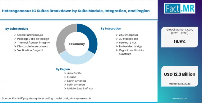
Heterogeneous Ic Suites Breakdown By Suite Module, Integration, And Region | Source: Fact.MR
| Attribute | Details |
|---|---|
| Quantitative Units | USD Billion |
| Market Definition | Software suites used to plan, implement, analyze and verify heterogeneous integrated circuits, including chiplet architecture, package and die co-design, thermal and power checks, die-to-die interconnect work and verification or signoff. |
| Suite Module | Chiplet architecture; Package / die co-design; Thermal / power integrity; Die-to-die interconnect; Verification / signoff |
| Integration | 2.5D interposer; 3D stacked die; Fan-out / RDL; Embedded bridge; Organic multi-chip substrate |
| End Market | AI / HPC; Networking; Automotive; Mobile / consumer; Aerospace / other |
| Design Automation | Rule-based EDA; Constraint-driven; AI-assisted; Automated closure; Generative exploration |
| Regions Covered | North America; Latin America; Western Europe; Eastern Europe; East Asia; South Asia & Pacific; Middle East & Africa |
| Countries Covered | Taiwan; Japan; USA; South Korea; UK |
| Key Companies Profiled | Cadence Design Systems, Inc.; Synopsys, Inc.; Siemens EDA; Keysight Technologies; Zuken Inc. |
| Forecast Period | 2026 to 2036 |
| Approach | Hybrid top-down and bottom-up approach using semiconductor design-suite revenue, advanced packaging indicators, foundry ecosystem activity, country adoption, user workflow analysis and provider portfolio review. |
How is the market segmented?
-
By Suite Module
- Chiplet architecture
- Package / die co-design
- Thermal / power integrity
- Die-to-die interconnect
- Verification / signoff
-
By Integration
- 2.5D interposer
- 3D stacked die
- Fan-out / RDL
- Embedded bridge
- Organic multi-chip substrate
-
By End Market
- AI / HPC
- Networking
- Automotive
- Mobile / consumer
- Aerospace / other
-
By Design Automation
- Rule-based EDA
- Constraint-driven
- AI-assisted
- Automated closure
- Generative exploration
-
By Region
- North America
- Latin America
- Western Europe
- Eastern Europe
- East Asia
- South Asia & Pacific
- Middle East & Africa