- Market Value (2025): USD 31.4 Bn
- Estimated Value (2026): USD 33.2 Bn
- Forecast Value (2036): USD 58.1 Bn
- CAGR (2026-2036): 5.8%
What is the Silicon Wafers Market forecast to be worth by 2036?
USD 33.2 Billion in 2026 to USD 58.2 Billion by 2036 at 5.8% CAGR.
- According to Fact.MR analysis, the silicon wafers market reached USD 31.4 Billion in 2025.
- The market is projected to rise from USD 33.2 Billion in 2026 to USD 58.1 Billion by 2036.
- Sales are forecast to grow at a 5.8% CAGR over 2026 to 2036 as memory and logic fabrication uses more qualified silicon substrates.
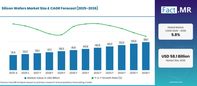
Factmr Silicon Wafers Market Forecast Global | Source: Fact.MR
| Year | Basis | Market value (USD billion) |
| 2025 | Actual | 31.4 |
| 2026 | Estimate | 33.2 |
| 2036 | Forecast | 58.1 |
| CAGR 2026 to 2036 | Forecast period | 5.8% |
Source: Fact.MR analysis. Updated Oct 14, 2026
What are the defining numbers behind Silicon Wafers Market growth?
An absolute chance of USD 25.0 Billion between 2026 and 2036.
- Demand Drivers in the Market
- Logic and memory factories need wafers with tight control of flatness and surface defects. SEMI reported 12,973 million square inches of worldwide silicon wafer shipments in 2025 [1], reflecting the scale of semiconductor substrate purchasing.
- Foundry operators are raising material needs for complex chips. SEMI measured 3573 million square inches of global wafer shipments in the second quarter of 2026 [2], as advanced compute and power-device needs supported ordering.
- Memory makers are managing wafer use around new capacity and high-bandwidth memory designs. The Semiconductor Industry Association reported USD 791.7 billion in worldwide semiconductor sales for 2025 [3], reflecting chip activity across many wafer-consuming categories.
- Key Segments Analyzed
- By Diameters: 300mm accounts for 62.4% share in 2026 because high-volume memory and logic plants run large-diameter processing lines.
- By Products: Memory represents 38.6% share in 2026 as substrate quality affects device yield across DRAM and flash fabrication.
- By Applications: Consumer Electronics capture 35.8% share in 2026 as phones and computers remain major downstream uses for silicon chips.
- Analyst Opinion at Fact.MR
- Shambhu Nath Jha, Principal Consultant at Fact.MR, states, “Silicon wafer suppliers compete on material consistency, surface quality, and their ability to meet strict customer specifications. Memory and logic manufacturers need dependable substrates because even small defects can affect costly fabrication steps.”
- Strategic Implications
- Wafer producers should focus technical support on documented flatness and defect performance for each customer process.
- Foundries should plan dual-source qualification early because substrate changes need engineering tests before routine production.
- Memory manufacturers should align purchasing schedules with fab loading and inventory use instead of assuming every chip sales increase produces immediate wafer orders.
- Equipment and materials companies should follow customer factory commissioning dates when planning capacity and staffing.
Brazil records the highest country CAGR at 6.4%, followed by Japan at 6.0% and the United States at 5.2%. Germany is forecast at 4.7%, while the United Kingdom records 4.3%. Each market has a different mix of chip design, manufacturing capacity and material supply relationships.
How does the Silicon Wafers Market break down by segment?
300mm accounts for 62.4%; Memory accounts for 38.6%; Consumer Electronics accounts for 35.8% in 2026.
Which wafer diameter holds the largest share?
300mm is projected to hold 62.4% share in 2026.
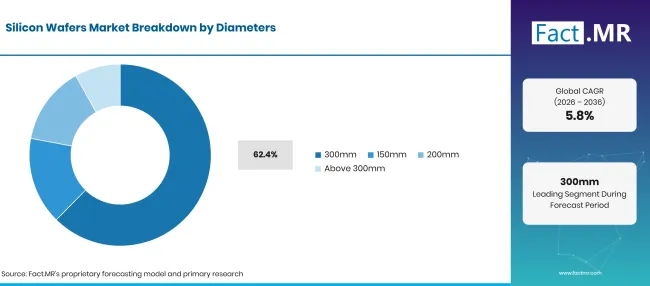
Factmr Silicon Wafers Market Breakdown Diameters | Source: Fact.MR
| Diameters | Share (2026) |
|---|---|
| 300mm (Leading segment) | 62.4% |
| Other segments combined | 37.6%* |
| Total | 100.0% |
Source: Fact.MR analysis. Updated Oct 14, 2026
Larger wafers lead high-volume chip factories process more devices on each substrate, although the final number depends on chip size and manufacturing yield. The 300mm format is standard in many advanced memory and logic processes. However, semiconductor producers also retain 200mm lines for established analog and power devices. A 150mm format serves selected older processes and specialist needs, while larger-than-300mm production remains outside mainstream commercial fab practice. SEMI linked the rise in 300mm shipments during 2025 to advanced logic and memory activity [7].
What leads the Products segment?
Memory is estimated to represent 38.6% share in 2026.
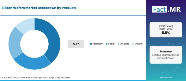
Factmr Silicon Wafers Market Breakdown Products | Source: Fact.MR
| Products | Share (2026) |
|---|---|
| Memory (Leading segment) | 38.6% |
| Other segments combined | 61.4%* |
| Total | 100.0% |
Source: Fact.MR analysis. Updated Oct 14, 2026
Memory production combines high wafer throughput with exact quality needs. A small change in substrate properties can affect yields across many individual memory cells. Logic customers have demanding inspection limits of their own, especially in advanced processors. Analog wafer purchasing follows longer product lifecycles and often uses mature equipment. The remaining product group covers silicon wafers entering other chip functions where electrical characteristics and treatment methods vary between factories.
How do Applications shape market sales?
Consumer Electronics is forecast to represent 35.8% share in 2026.
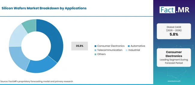
Factmr Silicon Wafers Market Breakdown Applications | Source: Fact.MR
| Products | Share (2026) |
|---|---|
| Memory (Leading segment) | 38.8% |
| Other segments combined | 61.2%* |
| Total | 100.0% |
Source: Fact.MR analysis. Updated Oct 14, 2026
Consumer electronics creates recurring chip volume through phones, computers and connected devices. Automotive chip designs place greater emphasis on product life and qualification history. Telecommunications applications need processors and supporting circuits for network equipment. Industrial customers often retain chips for long periods and value a stable supply of mature-node components. Differences in end use change wafer specs, but the direct customer for the wafer remains the chip manufacturer.
What is accelerating Silicon Wafers Market adoption, and what is holding it back?
Semiconductor manufacturing investment supports wafer purchasing; long qualification cycles and factory use restrain sales.
Drivers Impact Analysis
| DRIVER | (~) % IMPACT ON CAGR | GEOGRAPHIC RELEVANCE | IMPACT TIMELINE |
|---|---|---|---|
| New memory and logic production | +1.0% | East Asia, North America | Medium term (2–4 years) |
| Substrate quality requirements | +0.9% | Global | Long term (>= 4 years) |
| Factory capacity additions | +0.7% | North America, Europe | Long term (>= 4 years) |
| Stable mature-node operations | +0.6% | Global | Medium term (2–4 years) |
| AI-related chip activity | +0.5% | East Asia, North America | Short term (<= 2 years) |
Source: Fact.MR analysis. Updated Oct 14, 2026
Opportunity Impact Analysis
| OPPORTUNITY | (~) % IMPACT ON CAGR | GEOGRAPHIC RELEVANCE | IMPACT TIMELINE |
|---|---|---|---|
| Long-term supply contracts | +0.8% | Japan, USA | Medium term (2–4 years) |
| Lower-defect premium products | +0.7% | Global | Long term (>= 4 years) |
| Additional customer qualification | +0.5% | Europe, Asia | Long term (>= 4 years) |
| Stable 200mm supply | +0.4% | Global | Medium term (2–4 years) |
Source: Fact.MR analysis. Updated Oct 14, 2026
Restraints Impact Analysis
| RESTRAINT | (~) % IMPACT ON CAGR | GEOGRAPHIC RELEVANCE | IMPACT TIMELINE |
|---|---|---|---|
| Long customer approval periods | -0.8% | Global | Long term (>= 4 years) |
| Fixed capital and energy cost | -0.7% | Global | Medium term (2–4 years) |
| Uneven fab utilization | -0.6% | Global | Short term (<= 2 years) |
| Polysilicon and material quality risks | -0.4% | Global | Medium term (2–4 years) |
Source: Fact.MR analysis. Updated Oct 14, 2026
Which countries are scaling the Silicon Wafers Market through 2036?
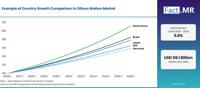
Factmr Silicon Wafers Market Growth Index | Source: Fact.MR
| Country | CAGR (2026–2036) |
|---|---|
| Brazil | 6.4% |
| Japan | 6.0% |
| USA | 5.2% |
| Germany | 4.7% |
| UK | 4.3% |
Source: Fact.MR analysis. Updated Oct 14, 2026
What supports Brazil’s silicon wafer outlook?
6.4% CAGR through 2036, shaped by semiconductor ecosystem development.
Brazil's semiconductor programs focus on domestic chip manufacturing and technical training. In December 2025, the Ministry of Science, Technology and Innovation reported R$267 million invested in projects of strategic details and communication technology in 2025 [8]. The same ministry said PADIS incentives for semiconductor activity can help companies prepare production facilities.
How is Japan supporting silicon wafer sales?
6.0% CAGR through 2036, supported by wafer supply expertise and chip investment.
Japan has developed expertise in silicon wafer production and is making new investments in advanced chip manufacturing. In April 2025, the Ministry of Economy, Trade and Industry announced over ¥802.5 billion in support for Rapidus [9]. As pilot projects progress, semiconductor materials suppliers are expected to benefit from the transition to repeatable factory orders.
What is shaping the United States market?
5.2% CAGR through 2036, supported by domestic materials and fab investment.
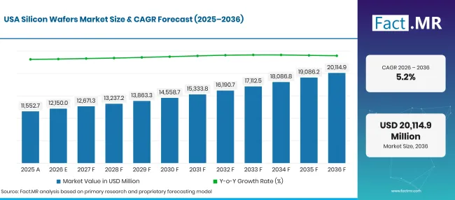
Factmr Silicon Wafers Market Forecast Usa | Source: Fact.MR
The United States is expanding its semiconductor manufacturing and materials base. In January 2025, the Department of Commerce announced up to USD 325 million for Hemlock Semiconductor to support semiconductor-grade polysilicon production [4]. The department separately announced up to USD 18 million for Edwards Vacuum during the same month [5]. These investments address upstream materials and factory equipment used in semiconductor production.
How does Germany’s semiconductor base affect growth?
4.7% CAGR through 2036, linked to industrial and automotive chip production.
Germany's silicon wafer outlook follows its automotive and industrial semiconductor base. Manufacturers use silicon substrates in power devices and control chips that must meet detailed reliable supply needs. Factory investment around Dresden is expected to open more openings for qualified wafer suppliers once new production lines are ready.
What supports the United Kingdom’s outlook?
4.3% CAGR through 2036, shaped by chip research and specialist device development.
The United Kingdom has a semiconductor sector focused on chip design and specialist research. In September 2025, the Department for Science, Innovation and Technology announced a £10 million fund for semiconductor innovation [6]. South Wales also has a specialist semiconductor ecosystem that supports practical materials and device work.
Who leads the Silicon Wafers Market?
Shin-Etsu Chemical and SUMCO are established semiconductor silicon wafer producers.
Shin-Etsu Chemical and SUMCO supply silicon wafers used in semiconductor manufacturing. They compete through product quality and long-term relationships with chip producers. Their product portfolios are focused on polished and processed wafers for chip production.
Which companies are the key providers?
Key companies include Shin-Etsu Chemical Co., Ltd.; SUMCO Corporation; Siltronic AG; GlobalWafers Co., Ltd.; and SK Siltron Co., Ltd.
- Shin-Etsu Chemical
- SUMCO
- Siltronic AG
- GlobalWafers Co., Ltd.
- SK Siltron Co., Ltd.
Bibliography
- [1] SEMI. (2026, February 10). SEMI reports 2025 annual worldwide silicon wafer shipments and revenue results.
- [2] SEMI. (2026, July 29). SEMI reports worldwide silicon wafer shipments increase 7.4% year-on-year in Q2 2026.
- [3] Semiconductor Industry Association. (2026, February 6). Global annual semiconductor sales increase 25.6% to $791.7 billion in 2025.
- [4] U.S. Department of Commerce. (2025, January 7). Department of Commerce announces CHIPS incentives award with Hemlock Semiconductor to help secure U.S. production capacity of semiconductor-grade polysilicon.
- [5] U.S. Department of Commerce. (2025, January 17). U.S. Department of Commerce announces CHIPS incentives awards with Corning, Edwards Vacuum, and Infinera to increase domestic production capacity of chips and equipment critical for U.S. technological leadership.
- [6] Department for Science, Innovation and Technology. (2025, September 24). New £10 million fund to support UK businesses to deliver next generation of semiconductors. GOV.UK.
- [7] SEMI. (2025, November 4). SEMI reports worldwide silicon wafer shipments increase 3% year-on-year in Q3 2025.
- [8] Ministério da Ciência, Tecnologia e Inovação. (2025, December 26). Entre chips, dados e inteligência artificial, 2025 marcou o avanço da soberania tecnológica do Brasil.
- [9] Ministry of Economy, Trade and Industry. (2025, April 1). Press Conference by Minister Muto (Excerpt).
This Report Answers
- The report examines how silicon wafer diameter affects semiconductor factory output and production costs.
- Segment analysis covers 300mm substrates alongside memory chips and consumer electronic applications.
- Country coverage compares Brazil, Japan, the USA, Germany and the UK across the forecast period.
- Competitive analysis separates semiconductor wafer producers from upstream silicon suppliers and solar wafer manufacturers.
- Supply analysis considers the effect of factory loading and substrate quality on repeat orders.
What does the Silicon Wafers Market cover?
The silicon wafers market covers semiconductor-grade silicon substrates supplied to chip fabrication businesses. Surface quality and agreed specs influence acceptance at each customer facility. Related markets include semiconductor-grade feedstock and photovoltaic wafers, although they should be analyzed separately.
What is included in the scope?
The scope covers finished silicon substrates that enter memory, logic and analog semiconductor processing. It considers diameter choice and the applications served by finished chips. The analysis also addresses regional factory activity and supplier qualification, including long approval periods for new wafer sources.
What is excluded from the scope?
Solar photovoltaic wafers are excluded from the semiconductor-device revenue boundary because their production routes and end markets differ. Compound semiconductor substrates, including silicon carbide and gallium arsenide, are also outside the core silicon wafer definition. Semiconductor manufacturing machines and bulk polysilicon are treated as related inputs rather than finished wafer sales.
How Was the Analysis Built?
The analysis draws on 120+ sources, 35+ company portfolios, 25+ countries, and more than 20 industry interviews.
- Primary Research: Primary research includes discussions with manufacturers, service providers, technology developers, distributors, end users, and subject-matter experts. These conversations examine purchasing priorities, product adoption, operational challenges, approval requirements, competitive positioning, and the factors that influence wider market acceptance.
- Desk Research: Desk research covers government statistics, regulatory publications, company filings, trade data, technical studies, industry associations, standards, public policy, and other authoritative sources. Every source used in the analysis is documented in the bibliography.
- Market Sizing and Forecasting: Market estimates combine historical performance, demand indicators, pricing and volume trends, segment shares, company participation, country-level growth, adoption patterns, investment activity, and barriers to market expansion.
- Data Validation and Update Cycle: Findings are validated by comparing primary interviews with public data, company activity, regulatory changes, trade patterns, and industry developments. Regular updates review new product launches, capacity changes, partnerships, approvals, and shifts in commercial adoption.
Segmentation
What is the report’s scope and coverage?
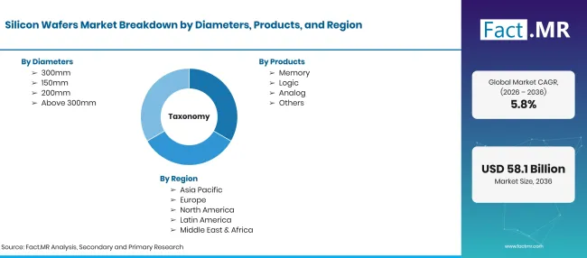
Factmr Silicon Wafers Market Taxonomy | Source: Fact.MR
| Attribute | Details |
|---|---|
| Quantitative Units | USD Billion in 2026 to USD Billion by 2036 at CAGR |
| Market Definition | Silicon wafer substrates used in semiconductor device fabrication, with photovoltaic wafers discussed only as an adjacent category. |
| Diameters | 150mm; 200mm; 300mm; Above 300mm |
| Products | Memory; Logic; Analog; Others |
| Applications | Consumer Electronics; Automotive; Telecommunication; Industrial; Others |
| Regions Covered | North America; Latin America; Western Europe; Eastern Europe; East Asia; South Asia & Pacific; Middle East & Africa |
| Countries Covered | Brazil; Japan; USA; Germany; UK |
| Key Companies Profiled | Shin-Etsu Chemical; SUMCO; Siltronic AG; LONGi Green Energy; SK Siltron Co., Ltd. |
| Forecast Period | 2026 to 2036 |
| Approach | Wafer area, semiconductor device fabrication, product mix and country conditions reviewed alongside official materials-sector evidence |
Source: Fact.MR analysis. Updated Oct 14, 2026
How is the market segmented?
-
By Diameters
- 300mm
- 150mm
- 200mm
- Above 300mm
-
By Products
- Memory
- Logic
- Analog
- Others
-
By Applications
- Consumer Electronics
- Automotive
- Telecommunication
- Industrial
- Others
-
By Region
- North America
- Latin America
- Western Europe
- Eastern Europe
- East Asia
- South Asia & Pacific
- Middle East & Africa
Frequently Asked Questions
How big is the silicon wafers market in 2026?
What is the market CAGR?
Which diameter leads silicon wafer sales?
Which product category leads?
Who are the main companies in the silicon wafers market?
Who worked on this report


Preview the report firsthand - request a free sample
Free SampleGet the brochure for pricing and purchase details
Download PDF