- Market Value (2025): USD 36.2 Mn
- Estimated Value (2026): USD 45.0 Mn
- Forecast Value (2036): USD 395.0 Mn
- CAGR (2026-2036): 24.3%
What is the Synthetic Defect Images Market forecast to be worth by 2036?
USD 45 million in 2026 to USD 395 million by 2036 at 24.3% CAGR.
- The synthetic defect images market reached USD 36.2 million in 2025 as fab teams expanded AI inspection tests around rare defect classes.
- Demand is projected to increase from USD 45.0 million in 2026 to USD 395.0 million by 2036.
- The market is forecast to record 24.3% CAGR from 2026 to 2036 owing to generated image libraries that train and validate defect classifiers.
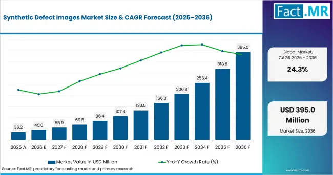
Synthetic Defect Images Market Value Analysis | Source: Fact.MR
What are the defining numbers behind Synthetic Defect Images Market growth?
USD 350 million absolute opportunity by 2036, led by Diffusion models and Optical defect images alongside Data-as-a-service delivery.
- Demand Drivers in the Market
- Fab inspection teams need synthetic defect libraries when real defects occur rarely and cannot train stable classifiers.
- Yield engineers require controlled optical and SEM examples so nuisance events do not overwhelm review queues. NIST reported in October 2025 that its SEM detection-limit study used six simulated image sets with 25 image-quality metrics to train and evaluate three AI models. This supports controlled image libraries for testing model behavior under noise and contrast changes.
- Mask shops use generated mask and reticle examples when pattern defects move below routine visual screening.
- AI teams need clean labels and traceable image provenance so model updates survive fab approval.
- Key Segments Analyzed
- By Generation Method: Diffusion models are expected to hold 44.0% share in 2026 owing to better control over rare defect patterns.
- By Data Type: Optical defect images are projected to account for 39.0% share in 2026 since inline inspection produces the widest review base.
- By Delivery: Data-as-a-service is anticipated to capture 55.0% share in 2026 due to curated libraries that reduce internal model maintenance.
- Analyst Opinion at Fact.MR
- Shambhu Nath Jha, Principal Consultant at Fact.MR, states, "Synthetic defect image programs draw attention because fabs cannot wait for every rare defect to appear naturally. Production use is expected to depend on close matches with real optical and SEM review. Suppliers should combine image physics, data governance and fab-specific validation evidence."
- Strategic Implications
- Fab engineering teams should test generated defect images against real review queues before connecting them to release decisions.
- Inspection software providers should document how synthetic images are labeled, filtered and updated after tool changes.
- Investors should separate semiconductor-specific image generation from generic computer vision data services.
- Procurement teams should require model drift checks when datasets move from pilot work into production support.
The USA is expected to record 26.32% CAGR through 2036 through digital twin funding and AI inspection work. South Korea is projected to post 25.76% CAGR as memory fabs refine defect review. Taiwan is anticipated to advance at 25.73% CAGR due to foundry scale. Israel and China are estimated at 25.66% CAGR. Japan is projected to reach 25.64% CAGR through metrology strength.
How does the Synthetic Defect Images Market break down by segment?
Diffusion models lead Generation Method at 44.0%; Optical defect images lead Data Type at 39.0%.
Which generation method dominates?
Diffusion models are projected to hold 44.0% share in 2026.
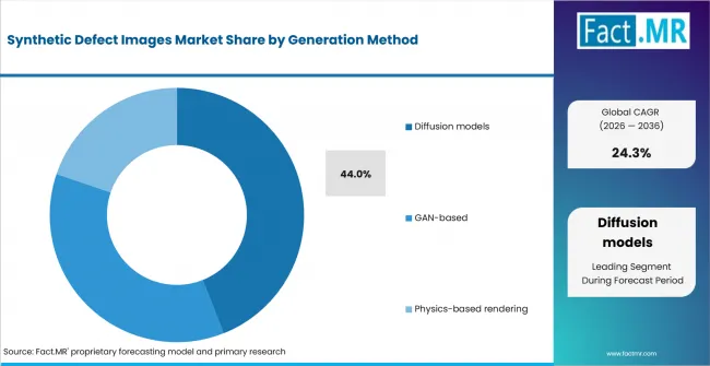
Synthetic Defect Images Market Analysis By Generation Method | Source: Fact.MR
Diffusion models lead the generation method segment because they create diverse, high-quality synthetic defect images with strong visual realism. Their flexibility supports inspection-model training, improves dataset diversity, and helps semiconductor manufacturers strengthen defect detection across advanced fabrication processes.
What leads the Data Type segment?
Optical defect images are expected to account for 39.0% share in 2026.
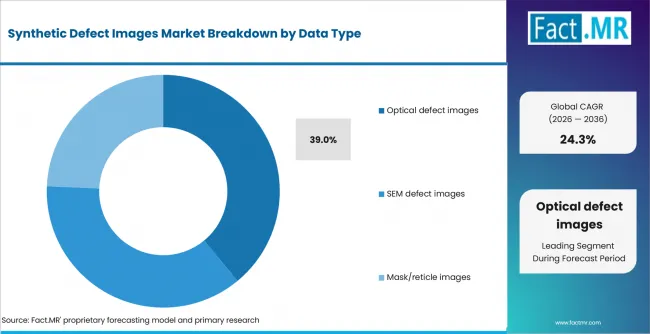
Synthetic Defect Images Market Analysis By Data Type | Source: Fact.MR
Optical defect images lead the data type segment because they are widely used in inline inspection and production monitoring. Their broad availability, rapid acquisition, and compatibility with automated inspection systems support efficient defect classification and yield improvement.
How does Delivery shape demand?
Data-as-a-service is anticipated to hold 55.0% share in 2026.
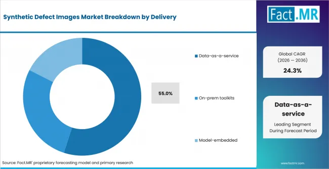
Synthetic Defect Images Market Analysis By Delivery | Source: Fact.MR
Data-as-a-service leads the delivery segment because semiconductor manufacturers increasingly require curated image libraries without maintaining complex generation infrastructure. This model enables faster deployment, scalable access to training datasets, and efficient support for AI-based inspection workflows across fabrication facilities.
What is accelerating Synthetic Defect Images Market adoption, and what is holding it back?
Scarce real defect data drives it; validation and data-control risk restrain it.
Drivers Impact Analysis
| DRIVER | (~) % IMPACT ON CAGR | GEOGRAPHIC RELEVANCE | IMPACT TIMELINE |
|---|---|---|---|
| Defect-class scarcity | +6.0% | USA, Taiwan, South Korea | Short term (<= 2 years) |
| SEM and eBeam review load | +4.8% | USA, Japan, Taiwan | Short term (<= 2 years) |
| AI inspection workflow expansion | +4.1% | USA, South Korea, China | Medium term (2-4 years) |
| Secure fab data collaboration | +3.2% | USA, Israel, East Asia | Medium term (2-4 years) |
| Mask and reticle defect modeling | +2.4% | Taiwan, Japan, China | Long term (>= 4 years) |
- Defect-class scarcity: Rare defect types give synthetic libraries a direct training role. Real wafers do not always produce enough examples for stable classifiers. Generated image sets are expected to help teams test edge cases before volume defects appear.
- SEM and eBeam review load: Nanoscale review creates many images that need careful interpretation.
- AI inspection workflow expansion: Inspection teams are shifting more defect sorting work into AI-assisted review. Applied Materials said in February 2025 that SEMVision H20 uses AI image recognition for buried nanoscale defects.
- Mask and reticle defect modeling: Patterning steps need defect examples that are costly to collect from live reticle events. Generated mask and reticle images help teams test detection rules before yield impact appears.
Opportunity Impact Analysis
| OPPORTUNITY | (~) % IMPACT ON CAGR | GEOGRAPHIC RELEVANCE | IMPACT TIMELINE |
|---|---|---|---|
| Diffusion model libraries | +2.1% | USA and Israel | Medium term (2-4 years) |
| Fab data collaboration | +1.8% | USA, South Korea, Taiwan | Medium term (2-4 years) |
| Model-embedded inspection assistants | +1.4% | USA and Japan | Long term (>= 4 years) |
| Synthetic SEM benchmark sets | +1.1% | Research and pilot fabs | Medium term (2-4 years) |
- Diffusion model libraries: Diffusion models create controlled variations that help inspection teams explore rare cases. Libraries with traceable labels are expected to gain value where fabs require repeatable test evidence.
- Fab data collaboration: Secure collaboration creates room for shared learning across manufacturers, materials firms and equipment providers. PDF Solutions announced an October 2025 collaboration with Lavorro for context-aware generative AI use in semiconductor fabs.
- Model-embedded inspection assistants: Inspection systems are adding AI features closer to the review flow. Embedded delivery is projected to grow where generated-image logic stays inside the approved tool chain.
Restraints Impact Analysis
| RESTRAINT | (~) % IMPACT ON CAGR | GEOGRAPHIC RELEVANCE | IMPACT TIMELINE |
|---|---|---|---|
| Real-to-synthetic gap | -2.0% | Global | Short term (<= 2 years) |
| IP and data-governance limits | -1.5% | USA, Taiwan, Israel | Medium term (2-4 years) |
| Validation cost | -1.1% | Smaller fabs | Medium term (2-4 years) |
| Export-control uncertainty | -0.8% | China and Japan | Long term (>= 4 years) |
- Real-to-synthetic gap: Generated images lose value when they do not reproduce optical noise, SEM artifacts or tool-specific defect signatures. Fabs therefore need comparison runs against real inspection queues. This extra proof step is expected to slow purchasing decisions.
- IP and data-governance limits: Defect images can expose process recipes and customer designs. Data teams must control who sees image libraries and how labels move across sites. These controls increase setup time for data-as-a-service contracts.
- Validation cost: Model validation requires image review, physical defect checks and documentation. Smaller fabs are expected to delay synthetic image programs when review staff are tied to production support. Tool vendors can reduce friction through clearer test packages.
- Export-control uncertainty: Cross-border image sharing faces more review where semiconductor equipment access is restricted. Policy checks slow cooperation between fabs and overseas software teams. On-prem delivery is expected to remain more attractive in these cases.
Which countries are scaling Synthetic Defect Images Market fastest?
- The country comparison spans 0.68 percentage point and forms a tight high-growth band across the forecast period.
- The USA remains 0.56 percentage point above South Korea through digital twin funding and strict fab validation.
- South Korea remains 0.03 percentage point above Taiwan as memory fabs widen defect review work.
- Taiwan remains 0.07 percentage point above Israel owing to foundry scale and AI-related semiconductor output.
- Japan closes the displayed range through metrology capability and semiconductor factory security standards.
Comparable CAGRs create different entry conditions because each country handles fab image data differently. Full report coverage includes North America, East Asia, Middle East, South Asia and Pacific, Europe and Latin America.
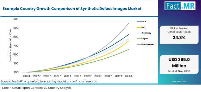
Example Country Growth Comparison Of Synthetic Defect Images Market | Source: Fact.MR
| Country | CAGR (2026-2036) |
|---|---|
| USA | 26.3% |
| South Korea | 25.76% |
| Taiwan | 25.73% |
| Israel | 25.66% |
| Japan | 25.64% |
What supports USA adoption?
26.3% CAGR, supported by digital twin funding and SEM image research. The Biden-Harris Administration awarded the Semiconductor Research Corporation Manufacturing Consortium Corporation
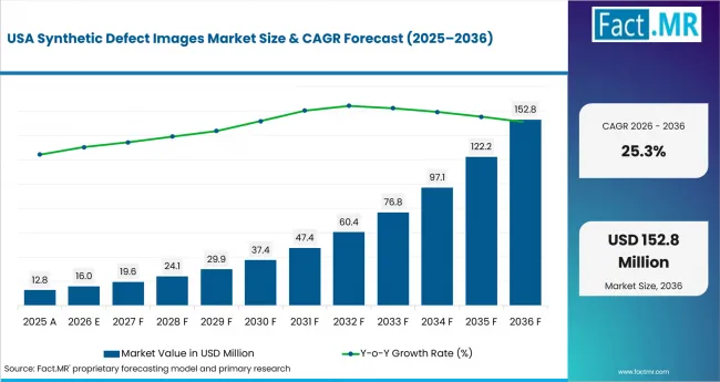
Synthetic Defect Images Market Country Value Analysis | Source: Fact.MR
$285M in January 2025 for the new CHIPS Manufacturing USA Institute for Digital Twins. Separately, a NIST study in April 2025 aims to improve the utility of the scanning electron microscope by refining models of electron scattering. Strong semiconductor R&D activity continues to support demand for AI-based inspection datasets.
How is South Korea scaling demand?
25.76% CAGR, driven by memory manufacturing and edge AI deployment.
Expanding memory production is expected to increase demand for synthetic inspection and defect-analysis data.
What is driving Taiwan’s growth from 2026 to 2036?
25.73% CAGR, backed by foundry scale and advanced packaging investment.
DGBAS reported in August 2025 that manufacturing output grew 17.24% in the second quarter of 2025. Large-scale foundry operations continue to strengthen demand for inspection datasets.
How is Israel developing demand?
25.66% CAGR, shaped by AI software depth and secure data analytics.
The Israel Innovation Authority reported in 2025 that around 1,500 deep-tech companies operate in the country. Strong AI innovation supports wider adoption of semiconductor data-generation technologies.
How does Japan perform?
25.64% CAGR, led by metrology capability and factory security discipline.
METI issued OT Security Guidelines for Semiconductor Device Factories in October 2025. Japan’s established precision manufacturing ecosystem continues to support advanced inspection and process-control technologies.
Who leads the Synthetic Defect Images Market?
PDF Solutions and Applied Materials show the direct relevance, while Synopsys strengthens adjacent AI workflow capability.
PDF Solutions supports semiconductor AI analytics through Exensio and Exensio Studio AI. Applied Materials connects the market to real defect review images through SEMVision H20. Synopsys contributes adjacent AI engineering automation through Synopsys.ai Copilot. Athinia Technologies supports secure semiconductor data collaboration. MakinaRocks adds manufacturing AI and machine-vision capability. Applied Materials introduced PROVision 10 in October 2025; the company said its cold-field-emission technology increases nanoscale image resolution by up to 50% and imaging speed by up to 10x versus conventional thermal-field-emission technology.
Which companies are the key providers?
Key companies include PDF Solutions, Inc., Applied Materials, Inc., Synopsys, Inc., NVIDIA Corporation, Siemens Digital Industries Software.
- PDF Solutions, Inc.
- Applied Materials, Inc.
- Synopsys, Inc.
- NVIDIA Corporation
- Siemens Digital Industries Software
Bibliography
- Applied Materials, Inc. (2025, February 19). Applied Materials accelerates chip defect review with next-gen eBeam system.
- Directorate General of Budget, Accounting and Statistics. (2025, August 15). GDP: Preliminary estimate for 2025Q2 and outlook for 2025–26.
- Directorate General of Budget, Accounting and Statistics. (2026, February 13). GDP: Preliminary estimate for 2025Q4, and outlook for 2026.
- Israel Innovation Authority. (2025, September 17). Israel Innovation Authority 2025 High-Tech Report.
- MakinaRocks Co., Ltd. (2025, March 13). MakinaRocks signs MOU with Siemens DI to drive edge AI innovation in manufacturing.
- Merck KGaA, Darmstadt, Germany. (2026, March 5). Research and development. In Annual Report 2025.
- Ministry of Economy, Trade and Industry. (2025, October 24). OT security guidelines for semiconductor device factories compiled in Japanese and English versions.
This Report Answers
- The report provides strategic intelligence on the Synthetic Defect Images Market across Generation Method and Data Type choices that shape semiconductor inspection model training.
- Segment analysis covers Diffusion models and Optical defect images as the share leaders within the 2026 market.
- Country outlook evaluates the USA and South Korea alongside Taiwan and Israel. Japan complete the growth comparison across the profiled markets.
- Competitive analysis profiles PDF Solutions and Applied Materials alongside Synopsys and Athinia. MakinaRocks and Onto Innovation complete the provider set.
- Delivery assessment covers Data-as-a-service and On-prem toolkits. Model-embedded delivery completes the commercial view.
What does the Synthetic Defect Images Market cover?
Synthetic defect images are used to train and validate semiconductor inspection models when real defect examples are limited or restricted.
The Synthetic Defect Images Market covers generated image libraries used near semiconductor defect inspection equipment. Coverage includes optical review images and SEM defect examples. Mask and reticle image generation is included when output supports classifier testing or yield review.
The scope also touches e-beam wafer inspection systems where high-resolution review images help compare generated and real defects. Data-as-a-service, on-prem toolkits and model-embedded delivery are included when they manage synthetic images for semiconductor use.
What is included in the scope?
The scope includes software and data-service workflows that create synthetic semiconductor defect images. Generation methods cover diffusion models, GAN-based systems and physics-based rendering. Data types include optical, SEM and mask or reticle defect images. Delivery covers data-as-a-service, on-prem toolkits and model-embedded generation.
Adjacent areas such as synthetic vision datasets are included only when the image output supports semiconductor defect training or validation. General object recognition datasets are outside scope when they do not address chip inspection evidence.
The market is related to synthetic data generation for industrial vision, but it is narrower because it focuses on semiconductor optical, SEM and mask or reticle defects.
What is excluded from the scope?
General computer vision datasets remain outside the scope when they do not address semiconductor inspection defects. Standalone inspection hardware revenue is excluded unless demand directly depends on synthetic image creation or validation. Natural-scene image generation and unrelated factory analytics are also excluded.
How Was the Analysis Built?
The analysis draws on 120+ sources, 35+ company portfolios, 25+ countries, and more than 20 industry interviews.
- Primary Research: Primary research includes discussions with semiconductor software providers, inspection teams, fab data leaders, procurement teams and subject-matter experts. These conversations examine training data needs, approval barriers, delivery models and commercial acceptance.
- Desk Research: Desk research covers government statistics, regulator publications, company pages, investor releases, technical studies, standards bodies and official semiconductor policy documents. Every source used in the analysis is documented in the bibliography.
- Market Sizing and Forecasting: Market estimates combine historical performance, inspection workflow adoption, image generation methods, delivery models, country-level growth, validation barriers and competitive positioning.
- Data Validation and Update Cycle: Findings are validated by comparing primary interviews with public data, company activity, policy changes and technical sources. Updates review data-service adoption, defect review tools and fab data-governance changes.
What is the report’s scope and coverage?
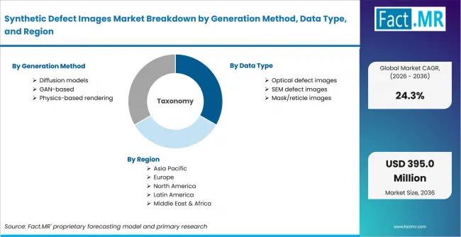
Synthetic Defect Images Market Breakdown By Generation Method, Data Type, And Region | Source: Fact.MR
| Attribute | Details |
|---|---|
| Quantitative Units | USD million |
| Market Definition | Software-generated, simulated or model-created defect image datasets used for semiconductor optical inspection, SEM review and mask or reticle inspection workflows |
| Generation Method | Diffusion models; GAN-based; Physics-based rendering |
| Data Type | Optical defect images; SEM defect images; Mask/reticle images |
| Delivery | Data-as-a-service; On-prem toolkits; Model-embedded |
| Regions Covered | North America; East Asia; Middle East; South Asia and Pacific; Europe; Latin America |
| Countries Covered | USA; South Korea; Taiwan; Israel; Japan |
| Key Companies Profiled | PDF Solutions, Inc.; Applied Materials, Inc.; Synopsys, Inc.; NVIDIA Corporation; Siemens Digital Industries Software |
| Forecast Period | 2026 to 2036 |
| Approach | Hybrid top-down and bottom-up approach using semiconductor inspection workflows; AI data-service adoption; optical and SEM review needs; mask and reticle defect requirements; country adoption patterns; official statistics; company portfolio review; validation risk and data-governance checks |
How is the market segmented?
-
By Generation Method
- Diffusion models
- GAN-based
- Physics-based rendering
-
By Data Type
- Optical defect images
- SEM defect images
- Mask/reticle images
-
By Delivery
- Data-as-a-service
- On-prem toolkits
- Model-embedded
-
By Region
- North America
- Latin America
- Western Europe
- Eastern Europe
- East Asia
- South Asia and Pacific
- Middle East & Africa