- Market Value (2025): USD 81.6 Mn
- Estimated Value (2026): USD 98.0 Mn
- Forecast Value (2036): USD 610 Mn
- CAGR (2026-2036): 20.1%
What is the Wafer Map Intelligence Market forecast to be worth by 2036?
USD 98 Million in 2026 and USD 610 Million by 2036, implying a 20.1% CAGR.
- The Wafer Map Intelligence Market was valued at USD 81.6 Million in 2025.
- Demand to increase from USD 98.0 Million in 2026 to USD 610 Million by 2036.
- The market is forecast to record a 20.1% CAGR from 2026 to 2036 and attributes the outlook to spatial yield analytics and fab-release requirements.
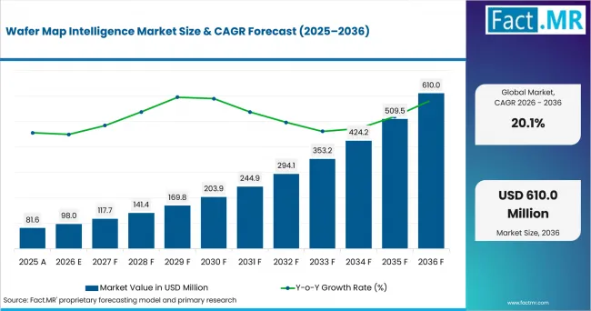
Wafer Map Intelligence Market Value Analysis | Source: Fact.MR
What are the defining numbers behind Wafer Map Intelligence Market growth?
Absolute opportunity is USD 512 Million from 2026 to 2036.
- Demand Drivers in the Market
- Foundry yield teams need spatial pattern recognition so recurring wafer signatures are separated from random loss during excursion review.
- IDM product engineers need clean map history because parametric drift is easier to trace when wafer and lot records stay linked.
- Memory manufacturers are expected to require faster map comparison as HBM and advanced memory flows add repeated wafer signatures.
- SEMI reported on April 7, 2026 that worldwide semiconductor manufacturing-equipment sales reached USD 135.1 billion in 2025, up 15.0% year over year.
- Key Segments Analyzed
- By Analytics Type: Spatial pattern recognition to hold 38.0% share in 2026 owing to its direct role in wafer signature recognition.
- By Deployment: Cloud SaaS to account for 49.0% share in 2026 because multi-site engineering teams need shared yield views.
- By Data Source: Bin maps to capture 41.0% share in 2026 as they remain the routine wafer-level yield record.
- By End User: Foundries to represent 40.0% share in 2026 due to high product mix and customer yield reporting.
- Analyst Opinion at Fact.MR
- Shambhu Nath Jha, Principal Consultant at Fact.MR, “Wafer map intelligence is drawing attention because fabs need pattern context instead of chart output. Production acceptance is expected to depend on how well software links maps with lot history and root-cause workflows. Better-qualified providers should combine clean data ingestion with spatial models and engineer-ready dashboards.”
- Strategic Implications
- Fab operations teams should connect wafer maps with tool and lot history before expanding automated disposition rules.
- Software vendors should prove that spatial models reduce manual review time without hiding the engineer decision path.
- NIST reported on January 3, 2025 that CHIPS for America awarded USD 285 million to Semiconductor Research Corporation Manufacturing Consortium Corporation to establish and operate the SMART USA digital-twin institute.
- Investors should separate wafer map intelligence platforms from generic manufacturing dashboards that lack semiconductor data depth.
Taiwan leads at 21.77% CAGR through semiconductor infrastructure and advanced pilot-line development. The USA follows at 21.74% as digital-twin R&D and advanced-packaging support strengthen adoption. South Korea reaches 21.60% through memory strength and semiconductor exports. China records 21.56% through integrated-circuit production scale. Japan posts 21.46% through advanced-node policy support, while Malaysia reaches 21.45% through OSAT depth and electronics investment.
How does the Wafer Map Intelligence Market break down by segment?
Spatial pattern recognition to lead Analytics Type at 38.0% and Cloud SaaS to lead Deployment at 49.0%.
Which Analytics Type dominates?
Spatial pattern recognition is expected to account for 38.0% share in 2026.
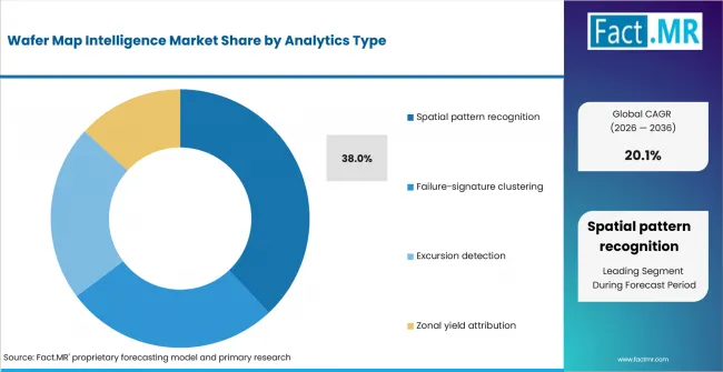
Wafer Map Intelligence Market Analysis By Analytics Type | Source: Fact.MR
Spatial pattern recognition leads the Analytics Type segment because fabs need fast separation between systematic and random yield loss. It helps engineering teams recognize recurring wafer signatures, compare spatial patterns across lots and connect abnormal map behavior with process conditions before yield issues spread across production.
What leads the Deployment segment?
Cloud SaaS is projected to hold 49.0% share in 2026.
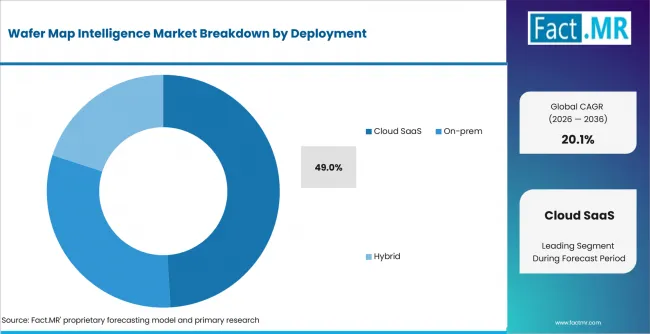
Wafer Map Intelligence Market Analysis By Deployment | Source: Fact.MR
Cloud SaaS leads the Deployment segment because yield teams need shared access to wafer-map intelligence across fabs and subcontractors. Centralized platforms support cross-site comparison, collaborative review and faster access to production data without requiring engineering teams to rebuild separate analytics pipelines for every manufacturing location.
How does Data Source shape demand?
Bin maps are anticipated to lead with 41.0% share in 2026.
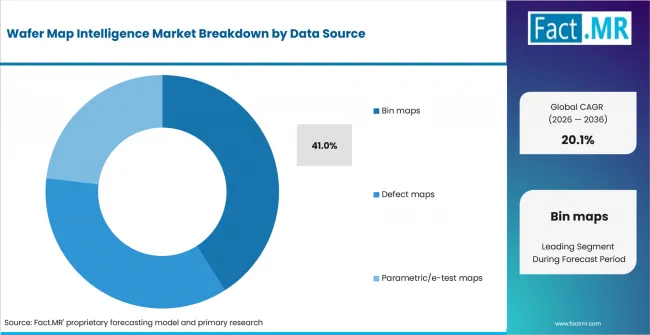
Wafer Map Intelligence Market Analysis By Data Source | Source: Fact.MR
Bin maps lead the Data Source segment because wafer-sort operations routinely generate spatial pass, fail and classification records. These maps support yield-pattern analysis and excursion review. SEMI reported on February 10, 2026 that worldwide silicon-wafer shipments increased 5.8% to 12,973 MSI in 2025.
What supports Foundries within End User?
Foundries are expected to hold 40.0% share in 2026.
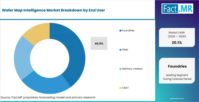
Wafer Map Intelligence Market Analysis By End User | Source: Fact.MR
Foundries lead the End User segment because high product mix creates numerous wafer-map patterns across customers, technologies and process nodes. Yield teams need consistent spatial analysis to compare signatures, identify recurring loss patterns and support customer reporting across complex semiconductor manufacturing environments.
What is accelerating Wafer Map Intelligence Market adoption, and what is holding it back?
Spatial yield learning drives it. Data access and model trust restrain it.
Drivers Impact Analysis
| Driver | (~) % IMPACT ON CAGR | Geographic Relevance | Impact Timeline |
|---|---|---|---|
| Spatial yield-pattern review | +5.2% | Taiwan, USA, South Korea | Short term (<= 2 years) |
| Cloud yield collaboration | +4.1% | Taiwan, USA, China | Short term (<= 2 years) |
| Advanced packaging feedback | +3.3% | USA, Taiwan, Malaysia | Medium term (2-4 years) |
| Memory and HBM test intensity | +2.8% | South Korea, Japan | Medium term (2-4 years) |
| Digital twin process modeling | +1.9% | USA, Japan | Long term (>= 4 years) |
- Spatial yield-pattern review: Map intelligence is expected to raise the value of wafer signatures during excursion review. Engineers can compare new loss patterns with earlier lots. That comparison is useful when root cause depends on location across the wafer.
- Cloud yield collaboration: Cloud SaaS is projected to support shared review across foundry, customer and subcontractor teams. Access control remains central because wafer data can reveal product behavior. Adoption is expected to favor vendors with clear permission rules.
- Advanced packaging feedback: Advanced packaging is anticipated to create new feedback loops between wafer sort and package test. Wafer-map context helps teams decide whether a package defect began upstream. The strongest commercial fit is expected in multi-die programs.
- Memory and HBM test intensity: Memory makers are expected to require fast comparison across repeated product lines. Similar wafer signatures can point to tool drift before yield loss becomes large. Analytics spending is expected to follow lines where review speed protects volume output.
- Digital twin process modeling: Digital twins are expected to expand demand for map-ready data sets. Wafer maps provide spatial context that process models often miss. Software that exports clean data is expected to gain more attention from engineering teams.
Opportunity Impact Analysis
| Opportunity | (~) % IMPACT ON CAGR | Geographic Relevance | Impact Timeline |
|---|---|---|---|
| AI-assisted wafer review | +2.1% | USA, Taiwan | Short term (<= 2 years) |
| OSAT map continuity | +1.6% | Malaysia, China | Medium term (2-4 years) |
| Recipe transfer analytics | +1.3% | Taiwan, South Korea, Japan | Medium term (2-4 years) |
| Customer yield portals | +0.9% | Foundry and OSAT clusters | Long term (>= 4 years) |
- AI-assisted wafer review: AI-assisted review is expected to shorten the first pass through dense map data. The benefit is practical when engineers still see the evidence behind a suggestion. Black-box results are expected to slow approval in production environments.
- OSAT map continuity: OSAT map continuity is projected to create opportunity after wafer sort data moves into package test. Shared map history can reduce repeated investigation. Demand is expected to build where customers need traceable die-level decisions.
- Recipe transfer analytics: Recipe transfer analytics is anticipated to help fabs compare map behavior when products move across tools. The value rises when older maps remain searchable. Engineers are expected to prefer platforms that retain context from earlier qualifications.
- Customer yield portals: Customer yield portals are forecast to make map evidence easier to discuss during foundry reviews. Controlled access is needed before external accounts see wafer-level records. The opportunity is expected to depend on security controls and useful summaries.
Restraints Impact Analysis
| Restraint | (~) % IMPACT ON CAGR | Geographic Relevance | Impact Timeline |
|---|---|---|---|
| Data access restrictions | -1.7% | USA, Taiwan, Japan | Short term (<= 2 years) |
| Model explainability gaps | -1.3% | Memory and foundry fabs | Short term (<= 2 years) |
| Legacy map formats | -0.9% | China, Malaysia | Medium term (2-4 years) |
| Subscription cost pressure | -0.6% | OSAT and smaller fabs | Long term (>= 4 years) |
- Data access restrictions: Wafer-map data often carries customer and product detail. Movement into cloud systems is expected to remain limited in some fabs. Vendors therefore need deployment models that fit strict data boundaries.
- Model explainability gaps: Model explainability is expected to restrain automated decisions when engineers cannot trace the reason for a flag. Fab teams still need a clear path from map pattern to action. Adoption is expected to move faster for explainable workflows.
- Legacy map formats: Legacy map formats are projected to slow rollout where factories hold records in separate systems. Cleaning old data adds time before analytics can start. The barrier is highest when fab, test and quality databases use different identifiers.
- Subscription cost pressure: Subscription cost pressure is anticipated to affect smaller fabs and OSAT sites. Yield teams must compare software spending with test hardware priorities. Vendors are expected to win more accounts when pricing follows clear usage value.
Which countries are scaling Wafer Map Intelligence Market fastest?
- The country comparison spans 0.32 percentage point and forms three practical growth bands across the forecast period.
- Taiwan remains 0.03 percentage point above the USA through semiconductor infrastructure and advanced pilot-line development.
- The USA remains 0.14 percentage point above South Korea through digital-twin R&D and advanced-packaging support.
- South Korea remains 0.04 percentage point above China as memory strength and semiconductor exports support wafer-map analytics demand.
- Japan remains 0.01 percentage point above Malaysia through advanced-node policy support and semiconductor investment.
- Malaysia closes the displayed range through OSAT depth and electrical and electronics investment.
Comparable CAGRs can create different entry conditions due to semiconductor infrastructure, data-access requirements, wafer-test intensity and local engineering depth. Full report coverage includes North America, Latin America, Europe, East Asia, South Asia and Pacific, Middle East and Africa.
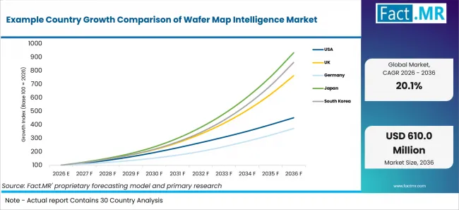
Example Country Growth Comparison Of Wafer Map Intelligence Market | Source: Fact.MR
| Country | CAGR (2026-2036) |
|---|---|
| Taiwan | 21.77% |
| USA | 21.74% |
| South Korea | 21.60% |
| Japan | 21.46% |
| Malaysia | 21.45% |
What supports Taiwan adoption?
21.77% CAGR, supported by semiconductor infrastructure and pilot-line development.
Taiwan’s growth is supported by semiconductor infrastructure and advanced pilot-line investment. MOEA reported on February 11, 2026 that the Advanced Semiconductor R&D Center forms part of a national infrastructure plan comprising three major pilot lines and a metrology validation laboratory, with the 12-inch advanced pilot line representing an investment of NT$3.77 billion.
What supports USA adoption?
21.74% CAGR, led by digital-twin R&D and advanced-packaging investment.
The USA’s growth reflects federal support for semiconductor digital-twin research and advanced manufacturing capabilities. NIST reported in January 2025 that CHIPS for America awarded USD 285 million to establish and operate SMART USA, supporting semiconductor digital-twin R&D and collaboration across the U.S. semiconductor ecosystem.
How is South Korea developing demand?
21.60% CAGR, driven by memory manufacturing and semiconductor-export activity.
South Korea’s growth is supported by its memory manufacturing base and semiconductor-export intensity. The Republic of Korea’s Ministry of Trade, Industry and Energy reported semiconductor exports of USD 73.27 billion in the first half of 2025, up 11.4% year over year.
How does Japan perform?
21.46% CAGR, supported by advanced-node policy and semiconductor investment.
Japan’s growth reflects continued government support for advanced semiconductor development. METI reported on June 5, 2026 that the Government of Japan had executed a JPY 150 billion investment in Rapidus through the Innovation Platform Agency, Japan (IPA).
What supports Malaysia’s growth?
21.45% CAGR, backed by OSAT depth and electronics investment.
Malaysia’s growth reflects its established electrical and electronics ecosystem and strong position in semiconductor assembly and testing. MIDA reported in May 2026 that Malaysia’s electrical and electronics ecosystem secured RM28.5 billion in approved investments in 2025, supporting continued semiconductor-sector expansion.
Who leads the Wafer Map Intelligence Market?
Key companies profile PDF Solutions, Inc., yieldWerx, NI OptimalPlus (Emerson), DR YIELD SOFTWARE & SOLUTIONS GMBH, Onto Innovation Inc. and Galaxy Semiconductor, Inc. as relevant providers based on semiconductor analytics portfolio fit.
yieldWerx reported in December 2025 that Ayar Labs engineers could view wafer maps, outlier signatures and correlations in its platform. PDF Solutions, Inc., NI OptimalPlus (Emerson), DR YIELD SOFTWARE & SOLUTIONS GMBH, Onto Innovation Inc. and Galaxy Semiconductor, Inc..
Which companies are profiled as relevant providers?
Key companies include PDF Solutions, Inc.; yieldWerx; NI OptimalPlus (Emerson); DR YIELD SOFTWARE & SOLUTIONS GMBH; Onto Innovation Inc.; and Galaxy Semiconductor, Inc.
- PDF Solutions, Inc.
- yieldWerx
- NI OptimalPlus (Emerson)
- DR YIELD SOFTWARE & SOLUTIONS GMBH
- Onto Innovation Inc.
- Galaxy Semiconductor, Inc.
Bibliography
- Ministry of Economic Affairs. (2026, February 11). MOEA breaks ground on Advanced Semiconductor R&D Center: Taiwan's first 12-inch pilot line to target AI, silicon photonics, and quantum technology.
- Ministry of Economy, Trade and Industry. (2026, June 5). Press conference by Minister Akazawa (Excerpt).
- Park, H. R. (2025, July 2). H1 exports shine despite US tariffs, chips post record high. Korea.net.
- National Bureau of Statistics of China. (2026, February 28). Statistical communiqué of the People's Republic of China on the 2025 national economic and social development.
- National Institute of Standards and Technology. (2025, January 3). Biden-Harris Administration awards Semiconductor Research Corporation Manufacturing Consortium Corporation $285M for new CHIPS Manufacturing USA Institute for Digital Twins, headquartered in North Carolina.
- yieldWerx. (2025, December 12). Ayar Labs and yieldWerx partner to streamline photonics test data analytics, delivering measurable results in just 30 days.
- Malaysian Investment Development Authority. (2026, May 7). MIDA positions talent at the centre of Malaysia's semiconductor growth.
This Report Answers
- The report provides strategic intelligence on the Wafer Map Intelligence Market across Analytics Type and Deployment choices that shape semiconductor yield workflows.
- Segment analysis covers Spatial pattern recognition and Cloud SaaS as share leaders within the 2026 market.
- Country outlook evaluates Taiwan and the USA alongside South Korea and China. Japan and Malaysia complete the growth comparison across the profiled markets.
- Competitive analysis profiles PDF Solutions, Inc. and yieldWerx alongside Optimal+ and DR YIELD SOFTWARE & SOLUTIONS GMBH. Onto Innovation Inc. and Galaxy Semiconductor, Inc. complete the provider set.
- Data-source assessment covers Bin maps and Defect maps. Parametric and e-test maps complete the data view for wafer-level analytics.
What does the Wafer Map Intelligence Market cover?
Wafer map intelligence platforms are used to read spatial yield patterns where die position, wafer history and test outcome determine the next engineering action.
The Wafer Map Intelligence Market covers software used for wafer-sort maps, defect maps and e-test records. Adjacent inspection workflows include e-beam wafer inspection systems and semiconductor defect inspection equipment, but only when output feeds wafer-level pattern analysis. Coverage includes cloud SaaS, on-prem and hybrid deployments. It also covers analytics for foundries, IDMs, memory makers and OSAT providers.
What is included in the scope?
The scope includes analytics that identify spatial patterns, failure clusters, excursions and zonal yield attribution across wafer data sets.
Coverage includes workflows connected to 3D semiconductor packaging, backside power metrology and HBM stack inspection when wafer-map evidence helps explain downstream yield behavior. It includes bin maps, defect maps and parametric or e-test maps. The scope also includes customer yield review tools where access is controlled and semiconductor data context is retained.
What is excluded from the scope?
General dashboards and unrelated factory software remain outside the scope unless they ingest wafer-map records and produce semiconductor yield decisions.
The scope excludes general industrial metrology, broad semiconductor robots and unrelated semiconductor CVD equipment spending unless the purchase is directly tied to wafer-map intelligence. It excludes simple charting tools without spatial pattern recognition. It also excludes assembly-only software unless wafer maps remain connected to package-test outcomes.
Packaging distortion tools such as panel warpage metrology and device-test systems such as SoC test platforms are considered adjacent. They are included only when their data is joined with wafer maps inside yield intelligence workflows.
How Was the Analysis Built?
The analysis draws on 120+ sources, 35+ company portfolios, 25+ countries, and more than 20 industry interviews.
- Primary Research: Primary research includes discussions with manufacturers, service providers, technology developers, distributors, end users, procurement teams, and subject-matter experts. These conversations examine purchasing priorities, product adoption, operational challenges, approval requirements, competitive positioning, and the factors that influence wider market acceptance.
- Desk Research: Desk research covers government statistics, regulatory publications, company filings, trade data, technical studies, industry associations, standards, public policy, and other authoritative sources. Every source used in the analysis is documented in the bibliography.
- Market Sizing and Forecasting: Market estimates combine historical performance, demand indicators, pricing and volume trends, segment shares, company participation, country-level growth, adoption patterns, investment activity, and barriers to market expansion.
- Data Validation and Update Cycle: Findings are validated by comparing primary interviews with public data, company activity, regulatory changes, trade patterns, and industry developments. Regular updates review new product launches, capacity changes, partnerships, approvals, procurement trends, and shifts in commercial adoption.
What is the report’s scope and coverage?
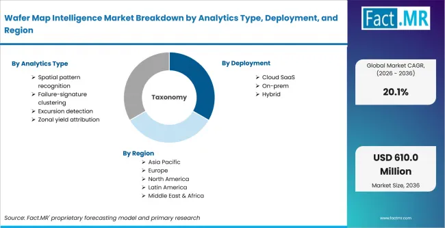
Wafer Map Intelligence Market Breakdown By Analytics Type, Deployment, And Region | Source: Fact.MR
| Attribute | Details |
|---|---|
| Quantitative Units | USD Million |
| Market Definition | Software platforms that ingest wafer maps and related semiconductor test data to detect spatial yield patterns, recurring failure signatures and excursion signals |
| Analytics Type | Spatial pattern recognition; Failure-signature clustering; Excursion detection; Zonal yield attribution |
| Deployment | Cloud SaaS; On-prem; Hybrid |
| Data Source | Bin maps; Defect maps; Parametric and e-test maps |
| End User | Foundries; IDMs; Memory makers; OSAT |
| Regions Covered | North America; Latin America; Europe; East Asia; South Asia and Pacific; Middle East and Africa |
| Countries Covered | Taiwan; USA; South Korea; China; Japan; Malaysia |
| Key Companies Profiled | PDF Solutions, Inc.; yieldWerx; NI OptimalPlus (Emerson); DR YIELD SOFTWARE & SOLUTIONS GMBH; Onto Innovation Inc.; Galaxy Semiconductor, Inc. |
| Forecast Period | 2026 to 2036 |
| Approach | Hybrid top-down and bottom-up approach using semiconductor equipment activity; wafer shipment data; foundry and memory production patterns; wafer-sort workflows; inspection records; test-data analytics; country adoption patterns and company portfolio review |
How is the market segmented?
-
By Analytics Type:
- Spatial pattern recognition
- Failure-signature clustering
- Excursion detection
- Zonal yield attribution
-
By Deployment:
- Cloud SaaS
- On-prem
- Hybrid
-
By Data Source:
- Bin maps
- Defect maps
- Parametric/e-test maps
-
By End User:
- Foundries
- IDMs
- Memory makers
- OSAT
-
By Region:
- North America
- Latin America
- Europe
- East Asia
- South Asia and Oceania
- Middle East and Africa