- Market Value (2025): USD 2.1 Bn
- Estimated Value (2026): USD 2.4 Bn
- Forecast Value (2036): USD 11.5 Bn
- CAGR (2026-2036):17.0%
What is the HBM Wafer on Wafer WoW Hybrid Bonding Market forecast to be worth by 2036?
USD 2.4 billion in 2026 to USD 11.5 billion by 2036 at 17.0% CAGR.
- The HBM Wafer on Wafer WoW Hybrid Bonding market was valued at USD 2.1 billion in 2025 as qualification work expanded around HBM packaging flows.
- Demand is projected to increase from USD 2.4 billion in 2026 to USD 11.5 billion by 2036.
- The market is forecast to record 17.0% CAGR from 2026 to 2036 as bonding accuracy becomes a purchase requirement.
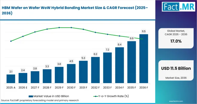
Hbm Wafer On Wafer Wow Hybrid Bonding Market Value Analysis | Source: Fact.MR
What are the defining numbers behind HBM Wafer on Wafer WoW Hybrid Bonding Market growth?
USD 9.2 billion absolute opportunity by 2036.
- Demand Drivers in the Market
- AI training and inference workloads are expected to raise memory bandwidth requirements in data center accelerator designs. The Ministry of Trade, Industry and Resources and the Ministry of Science and ICT reported 2025 ICT exports of USD 264.29 billion, up 12.4%, with semiconductor exports reaching USD 173.48 billion, up 22.1%, as AI data center investment lifted memory demand.
- Chiplet architectures are anticipated to raise demand for wafer-level bonding flows that shorten the path between memory and logic.
- Semiconductor supply planning is expected to push buyers toward qualified bonding capacity near memory and foundry clusters.
- Key Segments Analyzed
- By Bonding Solution: Wafer-on-Wafer Hybrid Bonding is expected to hold 56.0% share in 2026 because it fits high-volume wafer alignment needs.
- By Application: HBM3E Memory Manufacturing is projected to account for 44.0% share in 2026 as advanced HBM stacks need fine-pitch connections.
- By End User: Memory Manufacturers are anticipated to capture 41.0% share in 2026 since HBM output depends on repeatable stacking and inspection.
- By Manufacturing Stage: Wafer-level Bonding is estimated to represent 63.0% share in 2026 due to its position before final package validation.
- By Hybrid Bonding Technology: Copper-to-Copper Hybrid Bonding is forecast to hold 58.0% share in 2026 as direct metal paths support bandwidth density.
- Analyst Opinion at Fact.MR
- Shambhu Nath Jha, Principal Consultant at Fact.MR, states, "HBM wafer-on-wafer hybrid bonding is moving from specialist development work into a process requirement for AI memory architectures. Production acceptance is expected to depend on overlay control and surface preparation. Copper connection quality and inspection evidence are expected to matter more than bonding speed alone."
- Strategic Implications
- Equipment providers should show bonding results across wafer lots before procurement teams commit to wider tool placement.
- Memory manufacturers should coordinate bonding and metrology earlier in the HBM qualification cycle.
- Foundry and OSAT partners should reserve capacity for programs where wafer-level bonding is part of the release path.
- Investors should separate direct WoW hybrid bonding exposure from wider backend equipment activity.
Taiwan leads at 18.4% CAGR through foundry scale and HBM packaging qualification. South Korea follows at 17.9% as memory manufacturing supports hybrid bonding demand. The USA records 17.3% through AI infrastructure and semiconductor investment. Japan reaches 16.7% through materials and equipment depth. China posts 16.0% as domestic semiconductor programs add local process demand. Germany reaches 15.4% through automotive semiconductor use. Singapore closes the listed range at 14.8% through advanced packaging support and regional distribution.
How does the HBM Wafer on Wafer WoW Hybrid Bonding Market break down by segment?
Wafer-on-Wafer Hybrid Bonding is expected to lead Bonding Solution at 56.0% share in 2026. HBM3E Memory Manufacturing is projected to lead Application at 44.0% share in 2026.
Why does Wafer-on-Wafer Hybrid Bonding lead Bonding Solution?
Wafer-on-Wafer Hybrid Bonding is projected to account for 56.0% share in 2026.
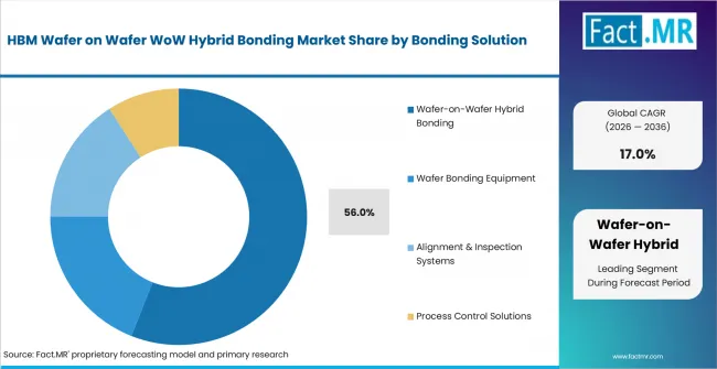
Hbm Wafer On Wafer Wow Hybrid Bonding Market Analysis By Bonding Solution | Source: Fact.MR
Wafer-level alignment gives this bonding solution a leading position since HBM and chiplet programs need fine-pitch connections across controlled surfaces. Other bonding routes remain useful when die flexibility is the main need. WoW bonding carries more value when memory makers need consistent placement before stack completion.
Why does HBM3E Memory Manufacturing lead Application?
HBM3E Memory Manufacturing is expected to hold 44.0% share in 2026.
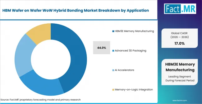
Hbm Wafer On Wafer Wow Hybrid Bonding Market Analysis By Application | Source: Fact.MR
HBM3E places high pressure on bonding accuracy since AI accelerators depend on memory bandwidth and compact interconnects. The application benefits from data center cpu and accelerator planning. Production teams are expected to test bonding quality together with inspection and thermal behavior. Micron said in March 2026 that its HBM4 36GB 12H was in high-volume production and delivered greater than 2.8 TB/s bandwidth with 20% better power efficiency, showing how the next memory generation keeps pressure on advanced HBM packaging flows.
Why do Memory Manufacturers lead End User?
Memory Manufacturers are projected to account for 41.0% share in 2026.
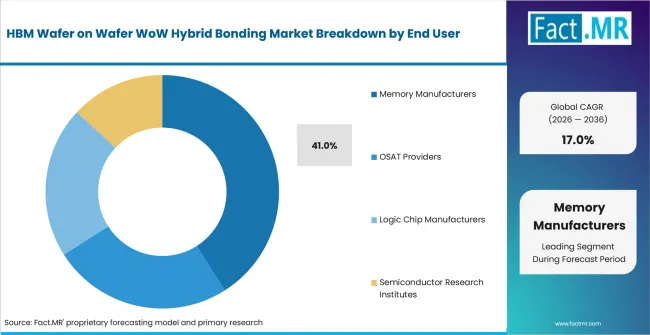
Hbm Wafer On Wafer Wow Hybrid Bonding Market Analysis By End User | Source: Fact.MR
Memory manufacturers have the closest exposure since HBM stack quality depends on bonding surfaces and interconnect integrity. Foundries and OSAT providers are expected to support adjacent demand when customer programs require outsourced packaging. Tool acceptance depends on yield evidence and repeatable wafer handling. SK hynix announced in September 2025 that it completed HBM4 development and readied mass production, with bandwidth doubled through 2,048 I/O terminals and power efficiency improved by more than 40% compared with the previous generation.
Why does Wafer-level Bonding lead Manufacturing Stage?
Wafer-level Bonding is anticipated to hold 63.0% share in 2026.
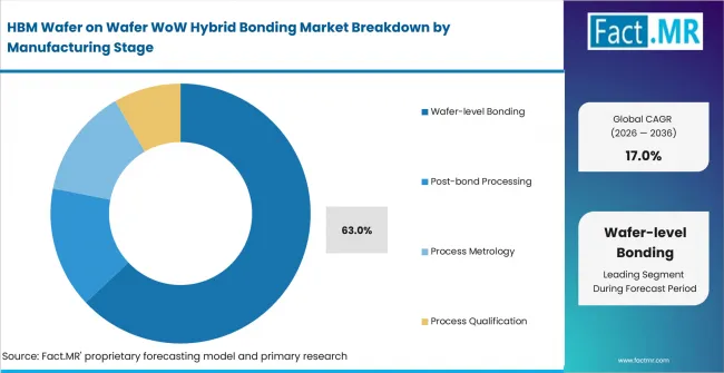
Hbm Wafer On Wafer Wow Hybrid Bonding Market Analysis By Manufacturing Stage | Source: Fact.MR
Wafer-level bonding leads where defects can move into later assembly and test. Buyers therefore place more weight on overlay control and clean wafer transfer. The stage is commercially sensitive because early bonding errors can make downstream inspection more expensive.
Why does Copper-to-Copper Hybrid Bonding lead Hybrid Bonding Technology?
Copper-to-Copper Hybrid Bonding is estimated to represent 58.0% share in 2026.
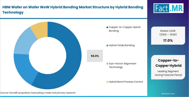
Hbm Wafer On Wafer Wow Hybrid Bonding Market Analysis By Hybrid Bonding Technology | Source: Fact.MR
Direct copper connection supports dense electrical paths for HBM and logic integration. The technology is valued where power efficiency and bandwidth density matter more than conventional interconnect spacing. Qualification remains difficult when surface planarity or contamination varies between wafers.
Thermal design remains part of the adoption case because AI memory packages add heat near dense compute components. Thermal management and thermal interface materials are expected to appear in the same supplier discussions.
What is accelerating HBM Wafer on Wafer WoW Hybrid Bonding Market adoption, and what is holding it back?
Demand is expected to rise through HBM bandwidth needs and chiplet integration. Growth is likely to be limited by capital cost; process complexity; and qualification time.
Drivers Impact Analysis
| DRIVER | (~) % IMPACT ON CAGR | GEOGRAPHIC RELEVANCE | IMPACT TIMELINE |
|---|---|---|---|
| Technology innovation and R&D | High | Global | 2026-2036 |
| Regulatory and policy drivers | Medium-High | North America; Europe | 2026-2032 |
| End-user industry expansion | High | Asia Pacific; MEA | 2026-2036 |
| Operational and cost efficiency | Medium | Global | 2026-2036 |
Source: Fact.MR analysis. Updated Aug 10, 2026
- Technology innovation and R&D: Hybrid bonding is expected to gain value as AI memory and chiplet programs move deeper into qualification.
- Regulatory and policy drivers: Regional semiconductor programs are expected to support local tool evaluation and supply-chain planning.
- End-user industry expansion: GPU servers and AI compute clusters are anticipated to lift demand for memory bandwidth and package density.
Opportunity Impact Analysis
| OPPORTUNITY | (~) % IMPACT ON CAGR | GEOGRAPHIC RELEVANCE | IMPACT TIMELINE |
|---|---|---|---|
| HBM4 and next-generation memory flows | High | Taiwan; South Korea; USA | Medium term (2-4 years) |
| Integrated bonding metrology | Medium-High | Taiwan and Japan | Medium term (2-4 years) |
| Regional advanced packaging support | Medium | USA; Germany; Singapore | Long term (>= 4 years) |
| Thermal-aware package design | Medium | Global | Long term (>= 4 years) |
Source: Fact.MR analysis. Updated Aug 10, 2026
- HBM4 and next-generation memory flows: Future HBM stacks are expected to increase the need for lower-pitch bonding and tighter process control.
- Integrated bonding metrology: Tool suppliers that connect bonding results with inspection data are expected to gain more proof during qualification.
- Thermal-aware package design: Electronic thermal materials are expected to influence supplier discussions when AI packages run at higher power density.
Restraints Impact Analysis
| RESTRAINT | (~) % IMPACT ON CAGR | GEOGRAPHIC RELEVANCE | IMPACT TIMELINE |
|---|---|---|---|
| Capital intensity and investment | Medium | Developing markets | 2026-2030 |
| Supply chain and raw material constraints | Medium | Global | 2026-2028 |
| Workforce and capability gaps | Low-Medium | Africa; Latin America | 2026-2036 |
Source: Fact.MR analysis. Updated Aug 10, 2026
- Capital intensity and investment: Hybrid bonding tools require high upfront spending before buyers can prove utilization across production programs.
- Supply chain and raw material constraints: Bonding performance depends on stable wafer preparation and clean material handling across each qualified step.
- Workforce and capability gaps: Process teams need bonding experience and inspection judgment before tools reach production scale.
Which countries are scaling HBM Wafer on Wafer WoW Hybrid Bonding Market fastest?
- The country comparison spans 3.6 percentage points and forms three practical growth bands across the forecast period.
- Taiwan remains 0.5 percentage point above South Korea through foundry scale and HBM packaging qualification.
- South Korea remains 0.6 percentage point above USA as memory manufacturing supports tool qualification.
- The USA remains 0.6 percentage point above Japan through AI infrastructure and semiconductor investment.
- Japan remains 0.7 percentage point above China through advanced materials and equipment capability.
- China remains 0.6 percentage point above Germany as domestic semiconductor programs add local process demand.
- Germany remains 0.6 percentage point above Singapore through automotive semiconductor and industrial electronics demand.
Comparable CAGRs can create different entry conditions due to fab scale and local engineering depth. Full report coverage includes North America; Latin America; Europe; East Asia; South Asia and Pacific; Middle East and Africa.
Hbm Wafer On Wafer Wow Hybrid Bonding Market Value Analysis | Source: Fact.MR
| Country | CAGR (%) |
|---|---|
| Taiwan | 18.4% |
| South Korea | 17.9% |
| USA | 17.3% |
| Japan | 16.7% |
| Germany | 15.4% |
| Singapore | 14.8% |
Source: Fact.MR analysis. Updated Aug 10, 2026
What is driving Taiwan’s growth from 2026 to 2036?
18.4% CAGR, supported by foundry scale and HBM packaging qualification.
Taiwan’s foundry ecosystem creates the strongest listed setting for wafer-level hybrid bonding. Local manufacturers are expected to evaluate tools through overlay control and surface preparation. The commercial value comes from shorter qualification loops near high-volume packaging activity.
How is South Korea developing demand?
17.9% CAGR, driven by memory manufacturing and equipment qualification activity.
South Korea’s memory base gives hybrid bonding a direct route into HBM production planning. Buyers are expected to focus on bond integrity and wafer handling consistency. Supplier access to engineering teams can shorten troubleshooting during process release.
What supports USA adoption?
17.3% CAGR, backed by AI infrastructure and semiconductor investment.
USA adoption is shaped by AI compute demand and domestic process development. The market is expected to favor equipment that can support pilot work before wider packaging use. Procurement teams are likely to link bonding readiness with inspection and reliability review.
How does Japan perform?
16.7% CAGR, led by advanced materials and equipment supply depth.
Japan’s materials and equipment base supports careful process qualification. Suppliers are expected to compete through surface treatment and wafer preparation know-how. This gives buyers a stronger support network when bonding defects require material-level review.
What supports Germany’s growth?
15.4% CAGR, driven by automotive semiconductor and industrial IoT demand.
Germany’s outlook reflects selective demand from automotive electronics and industrial semiconductor programs. Buyers are expected to adopt WoW bonding when package density affects computing performance. The country is likely to trail memory-heavy Asian clusters because HBM production exposure is narrower.
What supports Singapore’s growth?
14.8% CAGR, backed by advanced packaging support and regional distribution.
Singapore’s compact semiconductor cluster supports regional packaging and process service needs. Demand is expected to come from specialty fabs and nearby support operations. The market can grow when suppliers provide fast engineering response for qualified bonding flows. Singapore EDB said Micron broke ground in January 2025 on an HBM advanced packaging facility representing about USD 7 billion of investment, with operations scheduled to begin in 2026 and wider capacity expansion from calendar 2027.
Who leads the HBM Wafer on Wafer WoW Hybrid Bonding Market?
Applied Materials, Inc. show the clearest positioning in the listed provider set.
Tokyo Electron Limited and Lam Research Corporation strengthen the wider semiconductor equipment landscape. EV Group adds direct relevance through bonding and process-control activity. Applied Materials introduced new DRAM and advanced packaging systems in June 2026. EV Group unveiled an overlay metrology system for chiplet integration in September 2025.
Which companies are the key providers?
Key companies include Applied Materials, Inc.; Tokyo Electron Limited; Lam Research Corporation; EV Group; KLA Corporation; Onto Innovation Inc.
- Applied Materials, Inc.
- Tokyo Electron Limited
- Lam Research Corporation
- EV Group
- KLA Corporation
- Onto Innovation Inc.
Bibliography
- Applied Materials, Inc. (2026, June 25). Applied Materials introduces new systems to accelerate DRAM and advanced packaging for AI chips.
- EV Group. (2025, September 8). EV Group achieves breakthrough in hybrid bonding overlay control for chiplet integration.
- Ministry of Trade, Industry and Resources, & Ministry of Science and ICT. (2026, January 15). ICT exports post record annual performance in 2025.
- National Institute of Standards and Technology. (2025, January 16). U.S. Department of Commerce announces $1.4 billion in final awards to support the next generation of U.S. semiconductor advanced packaging.
- Micron Technology, Inc. (2026, March 16). Micron in high-volume production of HBM4 designed for NVIDIA Vera Rubin, PCIe Gen6 SSD and SOCAMM2.
- SK hynix Inc. (2025, September 12). SK hynix completes world’s first HBM4 development and readies mass production. The official SK hynix newsroom confirms both the date and headline.
- Micron Technology, Inc. (2025, January 8). Micron breaks ground on new HBM advanced packaging facility in Singapore.
- BE Semiconductor Industries N.V. (2026, January 12). BE Semiconductor Industries N.V. announces trading update.
- Onto Innovation Inc. (2026, February 19). Onto Innovation reports 2025 fourth quarter and full year results.
This Report Answers
- The report provides strategic intelligence on the HBM Wafer on Wafer WoW Hybrid Bonding Market across bonding and application choices that shape advanced memory packaging.
- Segment analysis covers Wafer-on-Wafer Hybrid Bonding and HBM3E Memory Manufacturing as the share leaders within the 2026 market.
- Country outlook evaluates Taiwan and South Korea alongside USA and Japan. China; Germany; and Singapore complete the growth comparison across the listed markets.
- Competitive analysis profiles Applied Materials, Inc. alongside Tokyo Electron Limited and Lam Research Corporation. EV Group; KLA Corporation; Onto Innovation Inc. complete the provider set.
- Technology assessment connects wafer-level bonding with accelerated processing and gpu asset planning where advanced memory affects AI hardware lifecycles.
What does the HBM Wafer on Wafer WoW Hybrid Bonding Market cover?
Wafer-on-wafer hybrid bonding covers wafer-level joining processes used to connect HBM and advanced chiplet architectures.
The HBM Wafer on Wafer WoW Hybrid Bonding Market covers bonding solutions used in high-bandwidth memory manufacturing and related advanced packaging flows. Coverage includes HBM3E Memory Manufacturing and Memory Manufacturers. Wafer-level Bonding and Copper-to-Copper Hybrid Bonding complete the main process view.
What is included in the scope?
T
he scope includes bonding tools and process-control needs that directly support HBM wafer-on-wafer hybrid bonding.
Coverage includes Bonding Solution; Application; End User; Manufacturing Stage; and Hybrid Bonding Technology. Regional coverage includes Taiwan; South Korea; USA; Japan; China; Germany; and Singapore.
What is excluded from the scope?
General semiconductor tools remain outside the scope when they do not support HBM wafer-on-wafer hybrid bonding.
The scope excludes unrelated backend assembly tools and general dry etch equipment. It excludes packaging activity without a clear HBM wafer-on-wafer bonding connection. Broader semiconductor demand is discussed only where it helps explain the adoption environment.
How Was the Analysis Built?
The analysis draws on 120+ sources and 35+ company portfolios. Coverage uses 25+ countries and more than 20 industry interviews.
- Primary Research: Primary research includes discussions with manufacturers and service providers. The interview base includes technology developers; distributors; end users; procurement teams; and subject-matter experts. These conversations examine purchasing priorities and product adoption. The review covers approval requirements and factors that influence wider market acceptance.
- Desk Research: Desk research covers government statistics and regulatory publications. The source base covers company filings; trade data; technical studies; industry associations; standards; public policy; and other authoritative sources. Every source used in the analysis is documented in the bibliography.
- Market Sizing and Forecasting: Market estimates combine historical performance and demand indicators. The forecast review uses pricing trends; segment shares; company participation; country-level growth; adoption patterns; investment activity; and barriers to market expansion.
- Data Validation and Update Cycle: Findings are validated by comparing primary interviews with public data and company activity. The review covers regulatory changes; trade patterns; and industry developments. Regular updates review new product launches; capacity changes; partnerships; approvals; procurement trends; and shifts in commercial adoption.
Segmentation
What is the report’s scope and coverage?
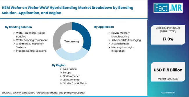
Hbm Wafer On Wafer Wow Hybrid Bonding Market Breakdown By Bonding Solution, Application, And Region | Source: Fact.MR
| Attribute | Details |
|---|---|
| Quantitative Units | USD billion |
| Market Definition | Wafer-level hybrid bonding used to join HBM wafers with fine-pitch electrical paths where surface preparation, overlay control, copper connection quality, and inspection evidence determine qualification |
| Bonding Solution | Wafer-on-Wafer Hybrid Bonding; Wafer Bonding Equipment; Alignment & Inspection Systems; Process Control Solutions |
| Application | HBM3E Memory Manufacturing; Advanced 3D Packaging; AI Accelerators; Memory-on-Logic Integration |
| End User | Memory Manufacturers; OSAT Providers; Logic Chip Manufacturers; Semiconductor Research Institutes |
| Manufacturing Stage | Wafer-level Bonding; Post-bond Processing; Process Metrology; Process Qualification |
| Hybrid Bonding Technology | Copper-to-Copper Hybrid Bonding; Hybrid Oxide Bonding; Sub-micron Alignment Technology; Hybrid Bond Process Control |
| Regions Covered | North America; Latin America; Europe; East Asia; South Asia and Pacific; Middle East and Africa |
| Countries Covered | Taiwan; South Korea; USA; Japan; China; Germany; Singapore |
| Key Companies Profiled | Applied Materials, Inc.; Tokyo Electron Limited; Lam Research Corporation; EV Group; KLA Corporation; Onto Innovation Inc. |
| Forecast Period | 2026 to 2036 |
| Approach | Hybrid top-down and bottom-up approach using HBM adoption, bonding tool qualification, memory packaging demand, wafer-level process controls, regional semiconductor clusters, company portfolio review, and country adoption patterns |
Source: Fact.MR analysis. Updated Aug 10, 2026
How is the market segmented?
-
By Bonding Solution
- Wafer-on-Wafer Hybrid Bonding
- Direct Wafer Bonding
- Hybrid Wafer Stacking
- Wafer Bonding Equipment
- High-precision Bonders
- Automated Wafer Bonders
- Alignment & Inspection Systems
- Optical Alignment Systems
- Bond Inspection Systems
- Process Control Solutions
- Automated Process Control
- Advanced Yield Management
- Wafer-on-Wafer Hybrid Bonding
-
By Application
- HBM3E Memory Manufacturing
- HBM4 Development
- AI Accelerator Integration
- Advanced 3D Packaging
- Chiplet Integration
- GPU Packaging
- AI Accelerators
- High-performance Computing
- Networking Processors
- Memory-on-Logic Integration
- 2.5D-3D Integration
- Next-generation HBM
- HBM3E Memory Manufacturing
-
By End User
- Memory Manufacturers
- DRAM Manufacturers
- Semiconductor Foundries
- OSAT Providers
- Advanced Packaging Companies
- GPU Manufacturers
- Logic Chip Manufacturers
- Hyperscale Infrastructure Providers
- Network Equipment Manufacturers
- Semiconductor Research Institutes
- Academic Research Centers
- Government Semiconductor Laboratories
- Memory Manufacturers
-
By Manufacturing Stage
- Wafer-level Bonding
- Pre-bond Alignment
- Precision Wafer Alignment
- Post-bond Processing
- Bond Inspection
- Production Bonding
- Process Metrology
- In-line Quality Inspection
- Failure Analysis
- Process Qualification
- Pilot Manufacturing
- Process Validation
- Wafer-level Bonding
-
By Hybrid Bonding Technology
- Copper-to-Copper Hybrid Bonding
- Direct Copper Bonding
- Oxide-to-Oxide Bonding
- Hybrid Oxide Bonding
- Surface Activated Bonding
- Plasma Activated Bonding
- Sub-micron Alignment Technology
- Infrared Alignment
- Bond Interface Inspection
- Hybrid Bond Process Control
- Real-time Bond Monitoring
- Artificial Intelligence-assisted Process Optimization
- Copper-to-Copper Hybrid Bonding
-
By Region
- North America
- Latin America
- Europe
- East Asia
- South Asia and Oceania
- Middle East and Africa
Frequently Asked Questions
How big is the HBM wafer on wafer WoW hybrid bonding market in 2026?
What is the CAGR of the HBM wafer on wafer WoW hybrid bonding market from 2026 to 2036?
Which bonding solution leads the HBM wafer on wafer WoW hybrid bonding market?
Which application leads the HBM wafer on wafer WoW hybrid bonding market?
Who are the leading companies in the HBM wafer on wafer WoW hybrid bonding market?
Who worked on this report


Preview the report firsthand - request a free sample
Free SampleGet the brochure for pricing and purchase details
Download PDF