- Market Value (2025): USD 7.8 Bn
- Estimated Value (2026): USD 8.9 Bn
- Forecast Value (2036): USD 31.6 Bn
- CAGR (2026-2036): 13.5%
What is the GPU Grade Silicon Wafer Market forecast to be worth by 2036?
USD 8.9 billion in 2026 to USD 31.6 billion by 2036 at 13.5% CAGR.
- The GPU grade silicon wafer market was valued at USD 7.8 billion in 2025 as AI accelerator and memory customers tightened wafer qualification requirements.
- Demand is forecast to increase from USD 8.9 billion in 2026 to USD 31.6 billion by 2036.
- The market is projected to expand at 13.5% CAGR from 2026 to 2036.
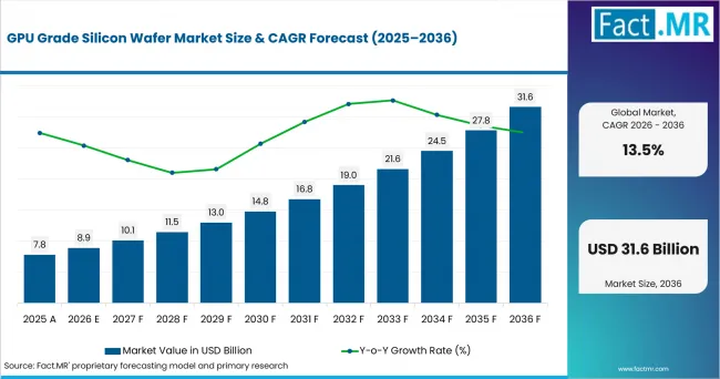
Gpu Grade Silicon Wafer Market Value Analysis | Source: Fact.MR
What are the defining numbers behind GPU Grade Silicon Wafer Market growth?
USD 22.5 billion absolute opportunity by 2036.
- Demand Drivers in the Market
- AI training and inference workloads are expected to raise demand for high-quality wafers that support GPU processors and HBM stacks.
- Chiplet-based designs are anticipated to widen use of silicon interposers and TSVs where substrate flatness matters early.
- Hyperscale cloud programs are likely to increase procurement of GPU server silicon and related accelerator inputs.
- Regional supply planning is expected to shape supplier selection as customers seek qualified wafer sources near foundry and OSAT programs.
- Key Segments Analyzed
- By Wafer Specification: 300 mm Prime Silicon Wafer is expected to hold 52.0% share in 2026 because mature 300 mm lines are the commercial route for GPU and memory programs.
- By Target Application: AI GPU Processors are projected to account for 45.0% share in 2026 as accelerator programs require stable wafer quality.
- By End-use Industry: Data Centers are anticipated to capture 43.0% share in 2026 since AI clusters remain the main demand channel.
- By Customer Type: Integrated Device Manufacturers are estimated to represent 47.0% share in 2026 due to direct process control.
- By Wafer Processing Technology: Epitaxial Wafer Processing is forecast to hold 42.0% share in 2026 as advanced devices require controlled layers.
- Analyst Opinion at Fact.MR
- Shambhu Nath Jha, Principal Consultant at Fact.MR, states, “GPU-grade wafer demand is shifting from general semiconductor volume toward qualification-led supply. AI accelerators and HBM packages need wafers that protect yield through front-end processing. Suppliers with process consistency and regional capacity are expected to hold stronger negotiating positions.”
- Strategic Implications
- Wafer suppliers need to prioritize low-defect 300 mm capacity and epitaxial process control before customer qualification windows tighten.
- Foundry and OSAT partnerships can strengthen supplier credibility by validating wafer performance through chiplet assembly and HBM stack inspection.
- Buyers are advised to assess regional sourcing depth because advanced computer programs expose supply risk when wafer qualification depends on a single location.
Taiwan leads at 14.8% CAGR through foundry scale and packaging proximity. The USA follows at 14.2% as AI infrastructure and supply planning support demand. South Korea reaches 13.8% through memory manufacturing. Japan posts 13.1% through materials and equipment depth. China records 12.5%. Germany reaches 11.9%. Singapore posts 11.3%.
How does the GPU Grade Silicon Wafer Market break down by segment?
300 mm Prime Silicon Wafer is expected to lead Wafer Specification at 52.0% share in 2026. AI GPU Processors are projected to lead Target Application at 45.0% share in 2026.
Which Wafer Specification dominates?
300 mm Prime Silicon Wafer is anticipated to account for 52.0% share in 2026.
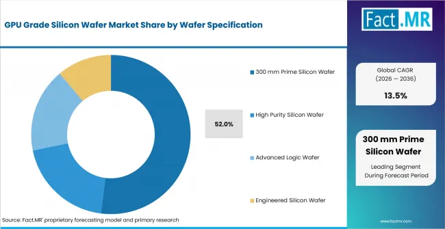
Gpu Grade Silicon Wafer Market Analysis By Wafer Specification | Source: Fact.MR
Its position reflects the installed base of mature 300 mm fabrication lines used for advanced GPU and memory production. Prime-grade material gives manufacturers the surface quality and defect control needed when high-value dies leave little room for wafer-level variation.
What leads the Target Application segment?
AI GPU Processors are projected to account for 45.0% share in 2026.
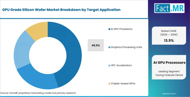
Gpu Grade Silicon Wafer Market Analysis By Target Application | Source: Fact.MR
This segment gains priority as accelerator dies demand tighter yield control and stronger package compatibility. Since memory-heavy AI workloads depend on high bandwidth and nearby interconnects, wafer quality becomes part of the broader processor-performance equation.
Why do Data Centers lead End-use Industry?
Data Centers are estimated to hold 43.0% share in 2026.
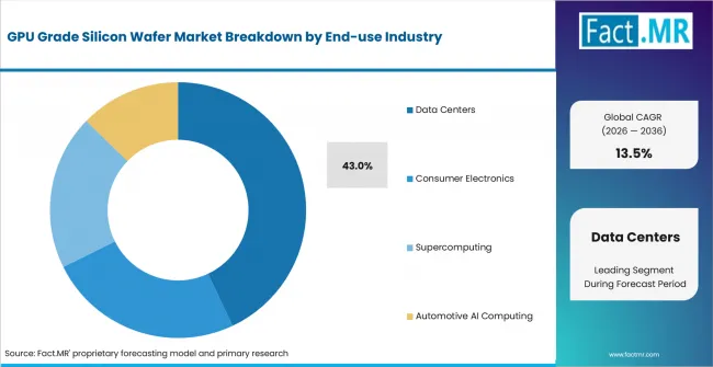
Gpu Grade Silicon Wafer Market Analysis By End Use Industry | Source: Fact.MR
Frequent accelerator upgrades keep data centers at the center of wafer demand. Their hardware roadmaps require qualified silicon inputs that can support dense compute, advanced packaging and cooling plans. This makes wafer selection closely linked with platform-level reliability.
What supports Integrated Device Manufacturers within Customer Type?
Integrated Device Manufacturers are forecast to account for 47.0% share in 2026.
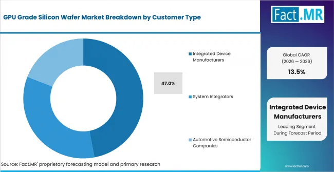
Gpu Grade Silicon Wafer Market Analysis By Customer Type | Source: Fact.MR
IDMs hold a strong position because they manage device design, process development and qualification under one operating structure. Their teams can test wafer behavior across multiple fabrication steps before moving from engineering lots to larger purchasing commitments.
How does Epitaxial Wafer Processing shape demand?
Epitaxial Wafer Processing is expected to lead with 42.0% share in 2026.
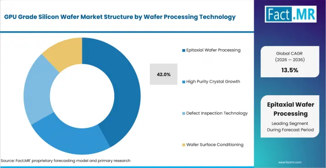
Gpu Grade Silicon Wafer Market Analysis By Wafer Processing Technology | Source: Fact.MR
Demand is shaped by the need for controlled layer growth before advanced patterning begins. For GPU and memory devices, epitaxial quality affects downstream process stability, defect inspection and performance consistency, linking wafer preparation directly with high-value semiconductor manufacturing.
What is accelerating GPU Grade Silicon Wafer Market adoption, and what is holding it back?
Demand is expected to rise through AI accelerator fabrication and HBM packaging. Growth is expected to be limited by capital intensity and lengthy customer approval cycles.
Drivers Impact Analysis
| DRIVER | (~) % IMPACT ON CAGR | GEOGRAPHIC RELEVANCE | IMPACT TIMELINE |
|---|---|---|---|
| AI GPU processor demand | High | Taiwan, USA, South Korea | 2026-2036 |
| Chiplet and 2.5D/3D packaging | High | Taiwan, South Korea, Japan | 2026-2036 |
| Hyperscale data center expansion | High | USA, Taiwan, Singapore | 2026-2036 |
| Regional wafer supply planning | Medium-High | USA, China, Germany | 2026-2032 |
| Thermal and automotive compute needs | Medium | Germany, Japan, USA | 2027-2036 |
- AI GPU processor demand: Accelerator designers are expected to put more weight on wafer consistency as larger dies make yield loss more expensive.
- Chiplet and 2.5D/3D packaging: Silicon interposers and TSVs are expected to make early wafer quality more visible during package release.
- Hyperscale data center expansion: Cloud operators are likely to increase demand for qualified GPU silicon as accelerator clusters expand.
Opportunity Impact Analysis
| OPPORTUNITY | (~) % IMPACT ON CAGR | GEOGRAPHIC RELEVANCE | IMPACT TIMELINE |
|---|---|---|---|
| Advanced packaging qualification | Medium-High | Taiwan, South Korea, USA | 2026-2036 |
| Epitaxial wafer process control | Medium | Japan, Germany, USA | 2026-2032 |
| GPU thermal package adjacency | Medium | USA, Germany, Japan | 2027-2036 |
| Regional wafer supply contracts | Medium | USA, East Asia, Singapore | 2026-2030 |
- Advanced packaging qualification: Suppliers that prove wafer behavior through advanced IC substrates and interposer assembly are expected to gain design-in access.
- Epitaxial wafer process control: Tighter layer control is expected to support premium wafer selection where GPU and memory designs need stable electrical behavior.
- GPU thermal package adjacency: Thermal-sensitive accelerators are expected to increase collaboration between wafer suppliers and thermal interface materials vendors.
Restraints Impact Analysis
| RESTRAINT | (~) % IMPACT ON CAGR | GEOGRAPHIC RELEVANCE | IMPACT TIMELINE |
|---|---|---|---|
| Capital intensity and investment | Medium | Developing markets | 2026-2030 |
| Supply chain and raw material control | Medium | Global | 2026-2028 |
| Workforce and capability gaps | Low-Medium | Africa, Latin America | 2026-2036 |
| Customer qualification cycles | Medium | Foundry and memory clusters | 2026-2032 |
- Capital intensity and investment: New wafer capacity requires long payback periods and stable customer commitments. Smaller suppliers are expected to delay expansion until utilization is clearer.
- Supply chain and raw material control: Semiconductor process chemicals and wafer inputs must meet tight purity rules. Procurement risk rises when customers cannot dual-qualify materials quickly.
- Customer qualification cycles: GPU customers require repeated testing before approving a wafer source. This slows supplier switching even when new capacity becomes available.
Which countries are scaling GPU Grade Silicon Wafer Market fastest?
- The country comparison spans 3.5 percentage points and forms three practical growth bands across the forecast period.
- Taiwan remains 0.6 percentage points above the USA through foundry concentration and advanced packaging depth.
- The USA remains 0.4 percentage points above South Korea because AI infrastructure and supply planning support wafer qualification.
- South Korea remains 0.7 percentage points above Japan through memory manufacturing and HBM-related process depth.
- Japan remains 0.6 percentage points above China with materials and equipment strength shaping supplier selection.
- China remains 0.6 percentage points above Germany as local semiconductor planning supports domestic wafer sourcing.
- Germany remains 0.6 percentage points above Singapore due to automotive semiconductor and industrial compute demand.
- Singapore closes the displayed range through advanced packaging support and regional distribution depth.
Comparable CAGRs create different entry conditions due to fab scale and customer approval processes. Full report coverage includes North America; Latin America; Europe; East Asia; South Asia and Pacific; Middle East and Africa.
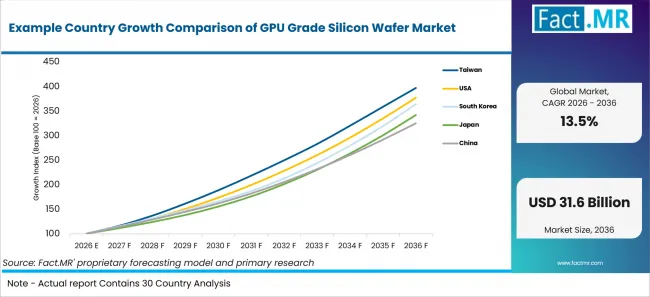
Example Country Growth Comparison Of Gpu Grade Silicon Wafer Market | Source: Fact.MR
| Country | CAGR (2026-2036) |
|---|---|
| Taiwan | 14.8% |
| USA | 14.2% |
| South Korea | 13.8% |
| Japan | 13.1% |
| Germany | 11.9% |
| Singapore | 11.3% |
What supports Taiwan adoption?
14.8% CAGR, backed by foundry scale and advanced packaging proximity.
Taiwan’s foundry base requires wafer suppliers to pass demanding approval work near high-volume GPU and HBM programs. Local engineering access is expected to shorten feedback loops for suppliers serving advanced production clusters.
How is the USA scaling demand?
14.2% CAGR, supported by AI infrastructure and domestic wafer supply planning.
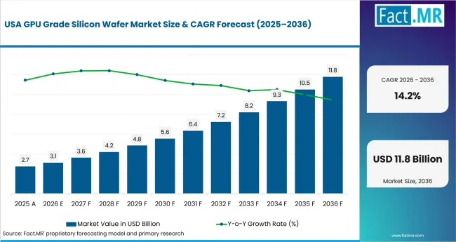
Gpu Grade Silicon Wafer Market Country Value Analysis | Source: Fact.MR
In the USA, data center accelerator demand is expected to keep wafer qualification tied to reliability and supply continuity. Buyers are likely to favor sources that match foundry requirements and long program timelines.
How is South Korea developing demand?
13.8% CAGR, driven by memory manufacturing and HBM-related process depth.
South Korea’s memory position places wafer quality close to HBM and accelerator package decisions. Suppliers must prove repeatable wafer behavior before memory-related compute programs move into wider use.
What supports Japan’s growth?
13.1% CAGR, led by materials capability and semiconductor equipment expertise.
Japan’s materials and equipment base gives customers deeper support during wafer evaluation. Surface quality and epitaxy performance are expected to decide supplier preference when advanced compute devices need stable inputs.
What supports Germany’s position?
11.9% CAGR, backed by automotive semiconductor and industrial IoT demand.
Germany’s demand reflects reliability-focused automotive electronics and industrial compute applications. Wafer suppliers are expected to benefit where automotive qualification discipline overlaps with advanced processor requirements.
How does Singapore perform?
11.3% CAGR, supported by advanced packaging and regional distribution.
Singapore’s compact semiconductor cluster places foundry activity near packaging and logistics support. This structure is expected to create selective demand for qualified wafers used in regional compute supply chains.
Who leads the GPU Grade Silicon Wafer Market?
Shin-Etsu Chemical has direct relevance through large-scale semiconductor silicon wafer supply. SUMCO and GlobalWafers add similar exposure through advanced wafer portfolios and regional capacity programs.
Siltronic and SK Siltron strengthen the high-purity 300 mm supply base. Wafer Works and Soitec add epitaxial wafer and engineered substrate exposure. Okmetic and National Silicon Industry Group add specialty wafer exposure. GlobalFoundries completes the profiled field through foundry-related demand
Which companies are the key providers?
Key companies include Shin-Etsu Chemical Co., Ltd., SUMCO Corporation, GlobalWafers Co., Ltd., Siltronic AG, SK Siltron Co., Ltd., Wafer Works Corporation, Soitec SA, National Silicon Industry Group Co., Ltd., and Ferrotec Holdings Corporation
- Shin-Etsu Chemical Co., Ltd.
- SUMCO Corporation
- GlobalWafers Co., Ltd.
- Siltronic AG
- SK Siltron Co., Ltd.
- Wafer Works Corporation
- Soitec SA
- National Silicon Industry Group Co., Ltd.
- Ferrotec Holdings Corporation
Bibliography
- SEMI (2026, April 29). SEMI reports worldwide silicon wafer shipments increase 13% year-on-year in Q1 2026.
- GlobalWafers Co., Ltd. (2024, December 17). GlobalWafers awarded U.S. CHIPS Act direct funding.
- Soitec SA (2024, December 4). Soitec and GlobalFoundries collaborate in the production of high-performance RF-SOI semiconductors.
- Ferrotec Holdings Corporation (2026, June 23). GlobalFoundries qualifies SLATE advanced packaging technology on 9SW platform for next-generation radio frequency applications.
This Report Answers
- The report explains how GPU-grade wafer demand changes across Wafer Specification and Target Application choices.
- Segment analysis reviews 300 mm Prime Silicon Wafer and AI GPU Processors as the leading 2026 categories.
- Country outlook compares Taiwan and the USA alongside South Korea and Japan. China, Germany and Singapore complete the growth view.
- Competitive analysis profiles Shin-Etsu Chemical and SUMCO alongside GlobalWafers and Siltronic. SK Siltron and Wafer Works form the next comparison pair. Soitec and Okmetic add engineered substrate and specialty wafer exposure. National Silicon Industry Group and GlobalFoundries complete the provider set.
- Process review covers Epitaxial Wafer Processing and Polished Wafer Processing. SOI processing and reclaimed wafer processing complete the core technology view. Wet process equipment is relevant where cleaning affects wafer release.
What does the GPU Grade Silicon Wafer Market cover?
GPU-grade silicon wafers are qualified substrates used in GPU processors, HBM-related devices and advanced compute packages.
The market covers prime silicon and epitaxial wafers used in compute-related semiconductor programs. Coverage extends to SOI wafers and high-resistivity wafers. Test and monitor wafers are included when they support compute qualification. Semiconductor defect inspection equipment is relevant where inspection affects GPU-grade release.
What is included in the scope?
GPU-grade wafers are used across integrated device manufacturers and foundries. Fabless semiconductor companies, OSAT providers and research institutes are included when their programs require qualified wafer inputs.
The scope includes Wafer Specification and Target Application alongside End-use Industry, Customer Type and Wafer Processing Technology. Coverage spans data centers and consumer electronics. Automotive, industrial automation and aerospace and defense applications are included when demand is connected to GPU-grade wafer use.
What is excluded from the scope?
General silicon wafers without GPU-grade qualification and unrelated semiconductor materials remain outside the scope.
The scope excludes commodity wafers that do not serve GPU or HBM programs. Accelerator and advanced compute routes are included only when wafer qualification is required. Packaging substrates and cooling parts remain outside the scope unless they directly affect wafer specification.
How Was the Analysis Built?
The analysis draws on 120+ sources, 35+ company portfolios, 25+ countries, and more than 20 industry interviews.
- Primary Research: Primary research includes discussions with manufacturers, service providers, technology developers, distributors, end users, procurement teams, and subject-matter experts. These conversations examine purchasing priorities, product adoption, operational challenges, approval requirements, competitive positioning, and the factors that influence wider market acceptance.
- Desk Research: Desk research covers government statistics, regulatory publications, company filings, trade data, technical studies, industry associations, standards, public policy, and other authoritative sources. Every source used in the analysis is documented in the bibliography.
- Market Sizing and Forecasting: Market estimates combine historical performance, demand indicators, pricing and volume trends, segment shares, company participation, country-level growth, adoption patterns, investment activity, and barriers to market expansion.
- Data Validation and Update Cycle: Findings are validated by comparing primary interviews with public data, company activity, regulatory changes, trade patterns, and industry developments. Regular updates review new product launches, capacity changes, partnerships, approvals, procurement trends, and shifts in commercial adoption.
What is the report's scope and coverage?
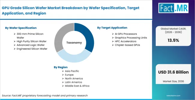
Gpu Grade Silicon Wafer Market Breakdown By Wafer Specification, Target Application, And Region | Source: Fact.MR
| Attribute | Details |
|---|---|
| Quantitative Units | USD billion in 2026 to USD billion by 2036 at CAGR |
| Market Definition | Semiconductor-grade silicon wafers qualified for GPU processors, HBM-related devices and advanced compute packages where surface quality, defect control and customer qualification determine use |
| Wafer Specification | 300 mm Prime Silicon Wafer; 300 mm Epitaxial Wafer; SOI Wafer; High-Resistivity Silicon Wafer; Test and Monitor Wafer |
| Target Application | AI GPU Processors; Graphics Workstation GPUs; Data Center Accelerators; Automotive AI Processors; Edge AI Devices |
| End-use Industry | Data Centers; Consumer Electronics; Automotive; Industrial Automation; Aerospace and Defense |
| Customer Type | Integrated Device Manufacturers; Foundries; Fabless Semiconductor Companies; OSAT Providers; Research Institutes |
| Wafer Processing Technology | Epitaxial Wafer Processing; Polished Wafer Processing; SOI Wafer Processing; Reclaimed Wafer Processing; Advanced Cleaning and Inspection |
| Regions Covered | North America; Latin America; Europe; East Asia; South Asia and Pacific; Middle East and Africa |
| Countries Covered | Taiwan; USA; South Korea; Japan; China; Germany; Singapore |
| Key Companies Profiled | Shin-Etsu Chemical Co., Ltd.; SUMCO Corporation; GlobalWafers Co., Ltd.; Siltronic AG; SK Siltron Co., Ltd.; Wafer Works Corporation; Soitec SA; National Silicon Industry Group Co., Ltd.; Ferrotec Holdings Corporation |
| Forecast Period | 2026 to 2036 |
| Approach | Hybrid top-down and bottom-up approach using wafer demand; GPU and HBM requirements; 300 mm qualification activity; foundry capacity; epitaxial processing; wafer processing technology review; country adoption patterns and company portfolio review |
How is the market segmented?
-
By Wafer Specification
- 300 mm Prime Silicon Wafer
- Polished 300 mm Wafer
- Epitaxial 300 mm Wafer
- High Purity Silicon Wafer
- N-type Silicon Wafer
- P-type Silicon Wafer
- Advanced Logic Wafer
- Low Defect Density Wafer
- High Resistivity Wafer
- Engineered Silicon Wafer
- Stress-engineered Wafer
- Low Warp Wafer
- 300 mm Prime Silicon Wafer
-
By Target Application
- AI GPU Processors
- High-performance GPU Computing
- AI Accelerator GPUs
- Graphics Processing Units
- Gaming GPUs
- Professional Visualization GPUs
- HPC Accelerators
- Exascale Computing
- High-bandwidth Memory Integration
- Chiplet-based GPUs
- Automotive AI Accelerators
- Embedded AI GPUs
- AI GPU Processors
-
By End-use Industry
- Data Centers
- Hyperscale Cloud Computing
- Artificial Intelligence Infrastructure
- Consumer Electronics
- Gaming Hardware
- Workstation Computing
- Supercomputing
- Government Research Laboratories
- Scientific Computing
- Automotive AI Computing
- Autonomous Vehicles
- Industrial Automation
- Data Centers
-
By Customer Type
- Integrated Device Manufacturers
- Fabless Semiconductor Companies
- Semiconductor Foundries
- GPU Manufacturers
- Original Equipment Manufacturers
- OSAT Providers
- System Integrators
- High-performance Computing Vendors
- Cloud Service Providers
- Automotive Semiconductor Companies
- Automotive Tier 1 Suppliers
- Industrial Electronics Manufacturers
- Integrated Device Manufacturers
-
By Wafer Processing Technology
- Epitaxial Wafer Processing
- Chemical Mechanical Polishing
- Epitaxial Silicon Growth
- High Purity Crystal Growth
- Neutron Transmutation Doping
- Oxygen Concentration Control
- Defect Inspection Technology
- Automated Wafer Inspection
- Surface Defect Detection
- Wafer Surface Conditioning
- Precision Surface Finishing
- Ultra-flat Wafer Processing
- Epitaxial Wafer Processing
-
By Region
- North America
- Latin America
- Western Europe
- Eastern Europe
- East Asia
- South Asia and Pacific
- Middle East & Africa