- Market Value (2025): USD 53.0 Mn
- Estimated Value (2026): USD 67 Mn
- Forecast Value (2036): USD 690 Mn
- CAGR (2026-2036): 26.3%
What is the MicroLED Transfer Metrology Market forecast to be worth by 2036?
USD 67 million in 2026 to USD 690 million by 2036 at a 26.3% CAGR.
- The MicroLED Transfer Metrology Market reached USD 53.0 million in 2025.
- Demand is projected to increase from USD 67 million in 2026 to USD 690 million by 2036.
- The market is forecast to record a 26.3% CAGR as display makers align transfer yield with optical inspection.
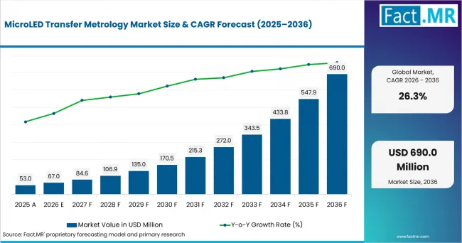
Microled Transfer Metrology Market Value Analysis | Source: Fact.MR
What are the defining numbers behind MicroLED Transfer Metrology Market growth?
USD 623 million absolute opportunity is expected by 2036.
- Demand Drivers in the Market
- Display makers need faster placement feedback since missing or shifted emitters reduce module yield before repair tools begin work.
- Panel OSATs need coordinate data owing to transfer flows that combine mass placement and repair.
- Equipment OEMs need metrology modules that exchange inspection data with transfer tools so placement errors are corrected faster.
- AR device teams need brightness uniformity checks because micro-displays expose small defects more clearly than larger panels.
- Electronics output supports adjacent process-control demand. The U.S. Census Bureau reported on 27 July 2026 that June 2026 new orders for computers and electronic products were USD 31.1 billion.
- Key Segments Analyzed
- By Metrology Technique: High-speed optical imaging is expected to hold 43.0% share in 2026 due to its fit with inline die location and visual defect review.
- By Measured Parameter: Placement accuracy is projected to account for 34.0% share in 2026 because transfer yield depends on emitter position before bonding and repair.
- By Throughput Class: Inline high-throughput systems are anticipated to capture 57.0% share in 2026 owing to production lines measuring defects during transfer flow.
- By Display Type: Micro-displays and AR are estimated to represent 36.0% share in 2026, supported by tight pixel layouts that require precise optical verification.
- By End User: Display makers are forecast to hold 48.0% share in 2026 as panel lines own the yield loss created by transfer and post-transfer repair.
- Analyst Opinion at Fact.MR
- Shambhu Nath Jha, Principal Consultant at Fact.MR, states, “Transfer metrology is becoming a yield-control layer, not a final inspection step. Suppliers are expected to gain attention when optical imaging, coordinate measurement and repair-loop data are connected inside the production line. The better platforms combine speed, placement traceability and defect classification in a format trusted by process engineers.”
- Strategic Implications
- Tool vendors should connect transfer, inspection and repair data so display makers trace every missing or shifted die to a process step.
- Metrology teams should document repeatability at sub-pixel scale since AR and wearable modules leave little tolerance for placement drift.
- Panel manufacturers should qualify inline recipes before adding capacity because late-stage optical binning is costlier than process-side correction.
- Equipment OEMs should support data exchange with repair tools, transfer bonders and factory systems to shorten process debug cycles.
Poland is projected to post 33.8% CAGR through 2036, supported by semiconductor-policy alignment. Finland is expected to record 33.0% CAGR due to photonics programs. The UK is anticipated to advance at 31.3%. South Korea is estimated to reach 30.7%, while Germany is forecast at 30.0%. The USA is projected at 22.2%, and Japan is anticipated at 20.8%.
How does the MicroLED Transfer Metrology Market break down by segment?
Inline high-throughput leads at 57.0%; Display makers lead End User at 48.0%.
Which Metrology Technique dominates?
High-speed optical imaging is expected to hold 43.0% share in 2026.
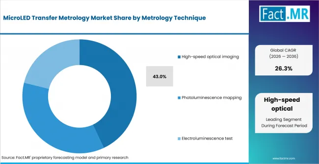
Microled Transfer Metrology Market Analysis By Metrology Technique | Source: Fact.MR
High-speed optical imaging leads because production lines need fast die-position feedback after transfer. Photoluminescence mapping remains useful before bonding, while electroluminescence test supports powered brightness checks. Onto Innovation Inc. launched the Dragonfly G5 on 16 March 2026 as an inspection and metrology platform with defect sensitivity down to 150 nm.
What leads the Measured Parameter segment?
Placement accuracy is projected to account for 34.0% share in 2026.
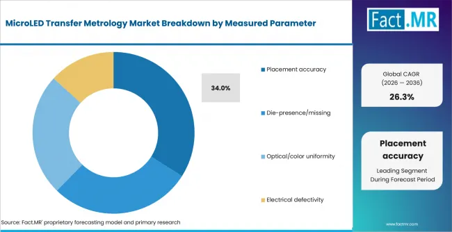
Microled Transfer Metrology Market Analysis By Measured Parameter | Source: Fact.MR
Placement accuracy leads due to the mechanical risk created when tiny emitters move from donor to target substrate. Die-presence checks remain necessary because one absent emitter is visible in a finished module. Transfer engineers prioritize placement accuracy before repair work starts.
How does Throughput Class shape demand?
Inline high-throughput is anticipated to lead with 57.0% share in 2026.
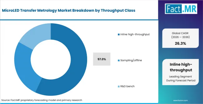
Microled Transfer Metrology Market Analysis By Throughput Class | Source: Fact.MR
Inline high-throughput systems lead owing to the need to catch transfer errors before rework becomes expensive. Sampling and offline tools fit R&D work where process windows are being tuned. V Technology Co., Ltd.’s February 2026 financial material identifies its FPD equipment business and lists inspection-related products among its key FPD offerings.
What supports Micro-displays and AR within Display Type?
Micro-displays and AR are estimated to hold 36.0% share in 2026.
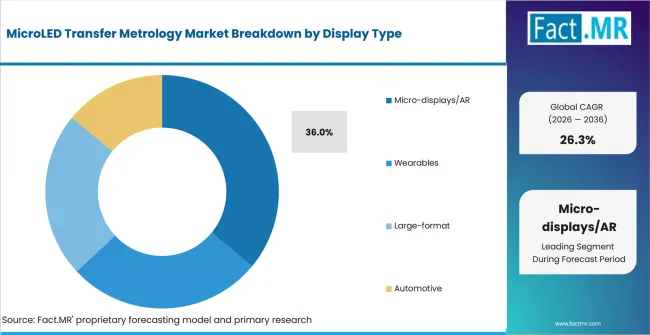
Microled Transfer Metrology Market Analysis By Display Type | Source: Fact.MR
Micro-displays and AR lead due to high pixel density and tight viewing-distance requirements. Wearables follow because brightness and low power draw suit compact screens.
What supports Display makers within End User?
Display makers are forecast to hold 48.0% share in 2026.
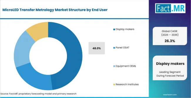
Microled Transfer Metrology Market Analysis By End User | Source: Fact.MR
Display makers lead because they own final panel yield and must connect transfer data to inspection and repair. Equipment OEMs embed metrology when customers ask for closed-loop transfer tools. At the opening of K-Display 2025 in August 2025, MOTIE reported participation by 143 companies and institutions across 582 booths.
What is accelerating MicroLED Transfer Metrology Market adoption, and what is holding it back?
Transfer-yield pressure drives it; qualification cost restrains it.
Drivers Impact Analysis
| Driver | (~) % Impact on CAGR | Geographic Relevance | Impact Timeline |
|---|---|---|---|
| Mass-transfer yield control | +2.5% | Global | Short term (<= 2 years) |
| AR and micro-display pixel density | +1.8% | USA, UK, Japan | Medium term (2-4 years) |
| Inline inspection and repair-loop integration | +1.5% | East Asia, Europe | Medium term (2-4 years) |
| Government-backed semiconductor pilot lines | +1.1% | USA, Poland, Finland | Long term (>= 4 years) |
| Display-equipment ecosystem expansion | +0.9% | South Korea, Japan | Long term (>= 4 years) |
- Mass-transfer yield control: Transfer defects become expensive once panels reach module assembly. Metrology suppliers are expected to gain demand when tools identify shifted or missing dies early in the line.
- AR and micro-display pixel density: Small display pixels make placement and color variation easier to see. Inspection recipes are anticipated to focus on coordinate accuracy and optical uniformity.
- Inline inspection and repair-loop integration: Production lines need inspection data that feeds repair decisions without separate review.
Opportunity Impact Analysis
| Opportunity | (~) % Impact on CAGR | Geographic Relevance | Impact Timeline |
|---|---|---|---|
| Closed-loop transfer and repair maps | +1.4% | Global | Medium term (2-4 years) |
| Micro-display process qualification | +1.2% | USA, UK, Japan | Short term (<= 2 years) |
| Panel-level metrology for larger substrates | +0.9% | South Korea, Japan | Long term (>= 4 years) |
| Photonics and compound-device transfer | +0.7% | Finland, Poland, Germany | Long term (>= 4 years) |
- Closed-loop transfer and repair maps: Tool makers are expected to grow share by linking placement coordinates with repair commands. That fit is clearest where mass transfer and repair are qualified together.
- Micro-display process qualification: AR and wearable programs need fast inspection before volume ramps. Supplier trials are anticipated to focus on repeatability across tiny pixel layouts.
- Panel-level metrology for larger substrates: Larger substrates require wide-field inspection and stable coordinate systems. Demand is projected to improve where MicroLED moves beyond small modules.
Restraints Impact Analysis
| Restraint | (~) % Impact on CAGR | Geographic Relevance | Impact Timeline |
|---|---|---|---|
| High qualification cost | -0.8% | Global | Short term (<= 2 years) |
| Limited MicroLED production scale | -0.6% | USA, Europe | Medium term (2-4 years) |
| Display capex caution | -0.5% | South Korea, Japan | Medium term (2-4 years) |
| Tool-skill shortage | -0.4% | Poland, Finland, UK | Long term (>= 4 years) |
- High qualification cost: Transfer metrology must prove speed and repeatability before production acceptance. Adoption is expected to slow when each recipe requires separate bonding and inspection validation.
- Limited MicroLED production scale: Many programs remain tied to pilots and premium devices. Equipment spending is anticipated to stay staged until yields support wider device programs.
- Display capex caution: Panel makers weigh MicroLED tools against existing OLED and LCD investments.
Which countries are scaling the MicroLED Transfer Metrology Market through 2036?
- The country comparison spans 13.0 percentage points and forms three practical growth bands across the forecast period.
- Poland remains 0.8 percentage point above Finland through semiconductor-policy alignment and a catch-up runway in photonics.
- Finland remains 1.7 percentage points above the UK as chip, photonics and quantum programs support R&D-led adoption.
- The UK remains 0.6 percentage point above South Korea through its semiconductor-company base and compound-semiconductor clusters.
- South Korea remains 0.7 percentage point above Germany through display production depth and local equipment qualification channels.
- Germany remains 9.2 percentage points above Japan through industrial electronics, optics capability and precision-equipment demand.
- The USA falls between Germany and Japan as packaging pilot investment supports process-control demand without matching East Asian display scale.
Comparable CAGRs create different entry conditions due to pilot-line access, display manufacturing depth, photonics skills and equipment qualification timelines. Coverage includes North America, Latin America, Western Europe, Eastern Europe, East Asia, South Asia & Pacific, Middle East & Africa.
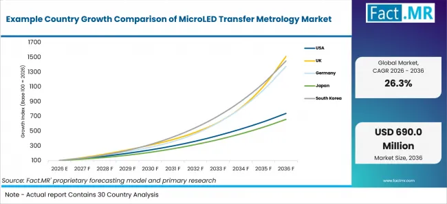
Example Country Growth Comparison Of Microled Transfer Metrology Market | Source: Fact.MR
| Country | CAGR (2026-2036) |
|---|---|
| Poland | 33.8% |
| Finland | 33.0% |
| United Kingdom | 31.3% |
| South Korea | 30.7% |
| Germany | 30.0% |
| USA | 22.2% |
| Japan | 20.8% |
What supports Poland adoption?
33.8% CAGR, supported by semiconductor-policy alignment and photonics capacity.
Poland is projected to record 33.8% CAGR through 2036 as its 2025 semiconductor policy gives pilot infrastructure a clearer public framework. Poland's Ministry of Digital Affairs published the final semiconductor-sector policy on 18 June 2025. The policy is organized around seven pillars, including infrastructure, investment and financing, and workforce and education.
How is Finland scaling demand?
33.0% CAGR, driven by photonics programs and chip ecosystem growth.
Finland is expected to post 33.0% CAGR through 2036 as photonics and chip programs support early metrology trials. Business Finland's Chips Campaign, updated on 20 October 2025, lists a EUR 40 million funding target and focuses on microelectronics, photonics and quantum technology.
What supports the United Kingdom’s growth?
31.3% CAGR, backed by semiconductor clusters and AR development demand.
The UK is anticipated to advance at 31.3% CAGR through 2036 as semiconductor clusters support AR and compound-device development. The current GOV.UK version of the Semiconductor Sector Study 2026 identifies 705 UK semiconductor companies.
How does South Korea perform?
30.7% CAGR, supported by display production depth and export scale.
South Korea is estimated to reach 30.7% CAGR through 2036 as panel makers and equipment suppliers stay close to display qualification cycles. MOTIR and MSIT reported in January 2026 that South Korea’s ICT exports reached USD 264.3 billion in 2025, up 12.4% year over year. At the opening of K-Display 2025 in August 2025, MOTIR reported participation by 143 companies and institutions across 582 booths; subsequent KDIA results listed 168 companies and 582 booths. South Korea’s concentration of display-panel, materials, parts and equipment companies may support access to specialized development and supplier networks.
What is supporting Germany’s adoption?
30.0% CAGR, led by industrial electronics and precision-equipment demand.
Germany is forecast to record 30.0% CAGR through 2036 as industrial electronics and optics capability support precision tool adoption. The Federal Ministry for Economic Affairs reported in February 2026 that December 2025 manufacturing orders rose 7.8% and electrical equipment orders rose 9.8%. German buyers are expected to favor metrology platforms that document repeatability for automotive, industrial and specialty display programs.
How is the USA developing demand?
22.2% CAGR, supported by semiconductor-packaging investment and electronics output.
The USA is projected to post 22.2% CAGR through 2036 as semiconductor-packaging pilots create adjacent demand for placement and inspection tools. The U.S. Department of Commerce finalized USD 1.4 billion in awards on 16 January 2025 for next-generation semiconductor advanced packaging.
How does Japan perform?
20.8% CAGR, driven by equipment depth and measuring-instrument production.
Japan is anticipated to reach 20.8% CAGR through 2036 through display-equipment depth and measuring-instrument capability. JEITA, citing METI, reported 2025 industrial electronic equipment production of JPY 3,416,604 million and electric measuring instrumentation production of JPY 523,884 million. In August 2025, Toray Engineering Co., Ltd. reported development of high-throughput laser-transfer technology designed to address mass-production requirements for advanced semiconductor and optical-integration devices.
Who leads the MicroLED Transfer Metrology Market?
Toray Engineering Co., Ltd. and KLA CORPORATION have the public evidence for MicroLED transfer/inspection workflows. Onto Innovation Inc. provides strong advanced-packaging inspection and metrology capability.
Toray Engineering Co., Ltd. has the clearest MicroLED transfer fit because its August 2025 development links laser transfer technology to MicroLED bonding. Onto Innovation Inc. is relevant through process-control inspection systems used for 2.5D and 3D applications. V Technology Co., Ltd. adds display-equipment heritage.
KLA CORPORATION has direct MicroLED mass-transfer inspection and metrology evidence: its MicroLED Yield Solutions material identifies Orbotech Flare MT Inspection and Metrology for in-scan measurement of LEDs during the mass-transfer workflow. Camtek Ltd. is better treated as an adjacent inspection/metrology supplier because its current public materials are strongest in semiconductor wafer, panel and advanced-packaging inspection rather than exact MicroLED transfer metrology. Competition is expected to center on inline speed, coordinate repeatability and repair-loop data integration.
Which companies are the key providers?
Key companies include Toray Engineering Co., Ltd., Onto Innovation Inc., V Technology Co., Ltd., Camtek Ltd., KLA CORPORATION.
- Toray Engineering Co., Ltd.
- Onto Innovation Inc.
- V Technology Co., Ltd.
- Camtek Ltd.
- KLA CORPORATION
Bibliography
- Business Finland. (2025, October 20). The Chips Campaign.
- Department for Science, Innovation and Technology. (2026, June 8). Semiconductor Sector Study 2026. GOV.UK.
- Federal Ministry for Economic Affairs and Energy. (2026, February 13). The Economic Situation in the Federal Republic of Germany in February 2026.
- Japan Electronics and Information Technology Industries Association. (2026, March 19). December 2025 production by the Japanese electronics industry.
- Ministry of Digital Affairs. (2025, June 18). Polityka dla sektora półprzewodników gotowa po konsultacjach [Semiconductor sector policy finalized after consultations]. GOV.PL.
- Ministry of Trade, Industry and Resources, & Ministry of Science and ICT. (2026, January 15). ICT exports post record annual performance in 2025.
- National Institute of Standards and Technology. (2025, January 16). U.S. Department of Commerce announces $1.4 billion in final awards to support the next generation of U.S. semiconductor advanced packaging.
- Onto Innovation Inc. (2026, March 16). Onto Innovation launches Dragonfly® G5 inspection system.
- Toray Engineering Co., Ltd. (2025, August 28). Bonding technology developed for ultra-thin semiconductors to deliver industry’s highest-level throughput—To support mass production of advanced semiconductors and next-generation photonic integrated circuits.
- U.S. Census Bureau. (2026, July 27). Monthly advance report on durable goods manufacturers’ shipments, inventories and orders: June 2026.
- Onto Innovation Inc. (2026, April 16). Onto Innovation’s Dragonfly® G5 system qualified for applications in 2.5D AI packaging.
This Report Answers
- The report explains where MicroLED transfer metrology is used across metrology technique and measured parameter.
- Segment analysis identifies high-speed optical imaging and inline high-throughput inspection as the main share positions.
- Country analysis reviews Poland, Finland, the UK, South Korea, Germany, the USA and Japan.
- Competitive analysis covers Toray Engineering Co., Ltd., Onto Innovation Inc., Camtek Ltd., V Technology Co., Ltd., KLA CORPORATION.
- Technology assessment reviews optical imaging, photoluminescence mapping and electroluminescence testing across transfer workflows.
What does the MicroLED Transfer Metrology Market cover?
Optical imaging, photoluminescence mapping and electroluminescence test systems used for transfer verification.
The MicroLED Transfer Metrology Market covers equipment and software that verify die placement and optical output after transfer. It overlaps with semiconductor defect inspection equipment when wafer or emitter inspection data is used before transfer. It also connects to flat panel displays where panel makers define the final visual acceptance window.
The market differs from general display inspection because the target is the MicroLED transfer event. Downstream demand is shaped by display driver ICs and augmented reality head-up display systems when small displays need tighter optical and electrical control.
What is included in the scope?
MicroLED transfer metrology systems used in display and micro-display production.
The scope includes inline and offline metrology for optical imaging, photoluminescence mapping and electroluminescence testing. It covers placement accuracy and missing-die checks across micro-displays, wearables, large-format panels and automotive displays. Related inspection logic is compared with optical sensor systems and industrial metrology tools where measurement repeatability shapes equipment selection.
The scope includes systems sold to display makers, panel OSATs, equipment OEMs and research institutes when configured for transferred MicroLED arrays. Adjacent manufacturing references include chip-on-board LED packages and HBM stack inspection where small placement errors also translate into yield loss.
What is excluded from the scope?
General display inspection and semiconductor process tools are outside the scope.
The scope excludes LCD, OLED and semiconductor inspection tools when they do not measure transferred MicroLED arrays. It excludes raw transfer bonders and repair equipment unless the quoted system includes metrology. Broader comparisons reference OLED display production or SoC test platforms only when boundary differences need clarification.
How Was the Analysis Built?
The analysis draws on 120+ sources, 35+ company portfolios, 25+ countries, and more than 20 industry interviews.
- Primary Research: Primary research includes discussions with manufacturers, service providers, technology developers, distributors, end users, procurement teams, and subject-matter experts. These conversations examine purchasing priorities, product adoption, operational challenges, approval requirements, competitive positioning, and the factors that influence wider market acceptance.
- Desk Research: Desk research covers government statistics, regulatory publications, company filings, trade data, technical studies, industry associations, standards, public policy, and other authoritative sources. Every source used in the analysis is documented in the bibliography.
- Market Sizing and Forecasting: Market estimates combine historical performance, demand indicators, pricing and volume trends, segment shares, company participation, country-level growth, adoption patterns, investment activity, and barriers to market expansion.
- Data Validation and Update Cycle: Findings are validated by comparing primary interviews with public data, company activity, regulatory changes, trade patterns, and industry developments. Regular updates review new product launches, capacity changes, partnerships, approvals, procurement trends, and shifts in commercial adoption.
What is the report’s scope and coverage?
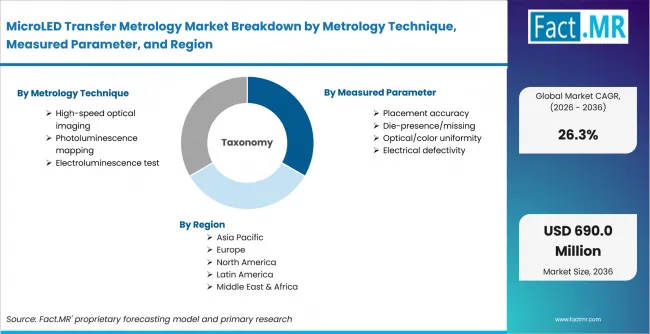
Microled Transfer Metrology Market Breakdown By Metrology Technique, Measured Parameter, And Region | Source: Fact.MR
| Attribute | Details |
|---|---|
| Quantitative Units | USD million |
| Market Definition | Equipment and software used to measure MicroLED transfer quality, including placement accuracy, die presence, optical uniformity and electrical defectivity. |
| Metrology Technique | High-speed optical imaging; Photoluminescence mapping; Electroluminescence test |
| Measured Parameter | Placement accuracy; Die-presence/missing; Optical/color uniformity; Electrical defectivity |
| Throughput Class | Inline high-throughput; Sampling/offline; R&D bench |
| Display Type | Micro-displays/AR; Wearables; Large-format; Automotive |
| End User | Display makers; Panel OSAT; Equipment OEMs; Research institutes |
| Regions Covered | North America; Latin America; Western Europe; Eastern Europe; East Asia; South Asia & Pacific; Middle East & Africa |
| Countries Covered | USA; United Kingdom; Germany; Japan; South Korea; Poland; Finland |
| Key Companies Profiled | Toray Engineering Co., Ltd., Onto Innovation Inc., V Technology Co., Ltd., Camtek Ltd., KLA CORPORATION |
| Forecast Period | 2026 to 2036 |
| Approach | Hybrid top-down and bottom-up approach using transfer-tool adoption, inspection attachment, display program timing and provider portfolio checks. |
How is the market segmented?
-
By Metrology Technique
- High-speed optical imaging
- Photoluminescence mapping
- Electroluminescence test
-
By Measured Parameter
- Placement accuracy
- Die-presence/missing
- Optical/color uniformity
- Electrical defectivity
-
By Throughput Class
- Inline high-throughput
- Sampling/offline
- R&D bench
-
By Display Type
- Micro-displays/AR
- Wearables
- Large-format
- Automotive
-
By End User
- Display makers
- Panel OSAT
- Equipment OEMs
- Research institutes
-
By Region
- North America
- Latin America
- Western Europe
- Eastern Europe
- East Asia
- South Asia & Pacific
- Middle East & Africa