- Market Value (2025): USD 155.2 Mn
- Estimated Value (2026): USD 182.0 Mn
- Forecast Value (2036): USD 900.0 Mn
- CAGR (2026-2036): 17.3%
What is the Backside Via Inspection Market forecast to be worth by 2036?
USD 182.0 million in 2026 to USD 900.0 million by 2036, at a 17.3% CAGR.
- The Backside Via Inspection Market crossed a valuation of USD 155.2 million in 2025, supported by demand from Foundries serving <50 nm workflows that require detecting opens, voids, mis-landing and sidewall defects in nano-scale vias etched from the wafer backside to buried frontside targets.
- Demand is projected to increase from USD 182.0 million in 2026 to USD 900.0 million by 2036.
- The market is forecast to record a 17.3% CAGR from 2026 to 2036 as the structures being inspected (imec reference implementation), alignment-inspection budget and defect classes remain central purchase reasons.
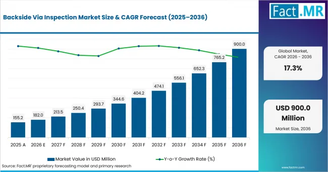
Backside Via Inspection Market Value Analysis | Source: Fact.MR
What are the defining numbers behind Backside Via Inspection Market growth?
USD 718.0 million absolute opportunity is expected by 2036.
- Demand Drivers in the Market
- The structures being inspected (imec reference implementation): Demand for backside via inspection tools is anchored in a validated reference structure: imec's backside power delivery implementation uses roughly 320 nm-deep nano-TSVs landing on buried power rails at a tight 200 nm pitch, processed after bonding the device wafer to a carrier and thinning the backside, with TEM confirming scaled FinFETs connect to both backside and frontside with no device degradation.
- Alignment-inspection budget: Inspection tools are being specified around an unusually tight alignment budget: nano-TSVs must land within about 10 nm of frontside targets per Cadence/IEDM guidance, an order of magnitude tighter than any packaging overlay, which means inspection must measure buried landing accuracy through silicon rather than just surface placement.
- Defect classes: Demand spans a defined set of defect classes adapted from hybrid-bond and TSV failure-analysis practice: voids and delamination at the wafer-bond interface screened by C-SAM, via-profile anomalies such as under-etch or not-through vias, mis-landing from overlay error, and copper/liner voids in via fill, each requiring a different inspection modality.
- X-ray capability trajectory: Demand for sub-micron 3D X-ray capability is projected to grow directly alongside backside power delivery adoption: nano-CT/laminography with under-100 nm voxels, already demonstrated on HBM micro-bumps and 1.5 micrometer hybrid bonds, is the capability trajectory Excillum and the IEEE Hybrid Bonding Symposium point to next for 200 nm-pitch backside vias.
- Key Segments Analyzed
- By Inspection Technique: E-beam inspection is projected to hold 32.0% share in 2026, supported by a clear process advantage: Electron-beam inspection provides the spatial resolution and voltage-contrast sensitivity needed to find tiny via opens, residue or landing failures. It can detect electrical behavior that is not visible as a large geometric defect.
- By Defect Type: Via voids are projected to hold 46.0% share in 2026, supported by a clear process advantage: A via void reduces conductive cross-section and can create a latent resistance or reliability failure after metallization. Because the feature is buried, early detection prevents a weak connection from escaping into final backside routing.
- By Via Dimension: <50 nm is projected to hold 42.1% share in 2026, supported by a clear process advantage: Dimensions below 50 nanometers correspond to nano-TSVs aimed at buried power rails and advanced-node backside contacts. At that scale, a few nanometers of residue, taper or mis-landing consume a large share of the available cross-section.
- By Inspection Mode: Inline sampling is projected to hold 43.7% share in 2026, supported by a clear process advantage: Inline sampling balances electron-beam sensitivity against the scan-time penalty of full-wafer coverage. It allows hotspots and process signatures to be monitored frequently while escalating suspect sites to deeper review.
- By End User: Foundries are projected to hold 29.0% share in 2026, supported by a clear process advantage: Foundries need a scalable inspection strategy because backside-via layouts and buried targets vary by customer design. They also must link inspection results to frontside process history and downstream metallization yield.
- Analyst Opinion at Fact.MR
- Shambhu Nath Jha, Sr. Consultant at Fact.MR, states, 'Buyers should evaluate the complete process sequence around detecting opens, voids, mis-landing and sidewall defects in nano-scale vias etched from the wafer backside to buried frontside targets. Technical review should focus on repeatability, integration, defect control and production throughput rather than a single headline specification. Suppliers that connect tool performance to measurable yield and qualification results are likely to build trust faster.'
- Strategic Implications
- Inspection should be placed before backside metallization commits more cost, with escalation paths for 3D localization and destructive confirmation.
- Equipment suppliers should document how their systems address the challenge of detecting opens, voids, mis-landing and sidewall defects in nano-scale vias etched from the wafer backside to buried frontside targets across production-representative wafers, panels, dies or packages.
- Procurement teams should compare sensitivity to backside-via opens, voids, misalignment and residue alongside wafer throughput, carrier handling, defect-classification performance and correlation to electrical test.
Taiwan is projected to record a 18.8% CAGR as leading foundry production, advanced packaging and a dense OSAT and substrate supply chain supports relevant capital spending; USA is projected to record a 19.1% CAGR as leading-edge logic, high-performance computing, federally supported semiconductor R&D and a large domestic equipment base supports relevant capital spending; South Korea is projected to record a 18.2% CAGR as high-volume memory, HBM and vertically integrated semiconductor manufacturing supports relevant capital spending; Israel is projected to record a 16.8% CAGR as advanced logic manufacturing and process-control R&D supports relevant capital spending; Japan is projected to record a 17.7% CAGR as semiconductor equipment, materials, inspection and memory-process expertise supports relevant capital spending; while Ireland is projected to record a 16.4% CAGR as European logic manufacturing and process-development investment supports relevant capital spending through 2036.
How does the Backside Via Inspection Market break down by segment?
E-beam inspection leads Inspection Technique with a 32.0% share, while Via voids accounts for 46.0% of Defect Type in 2026.
Why does E-beam inspection lead Inspection Technique?
E-beam inspection is projected to account for 32.0% share in 2026.
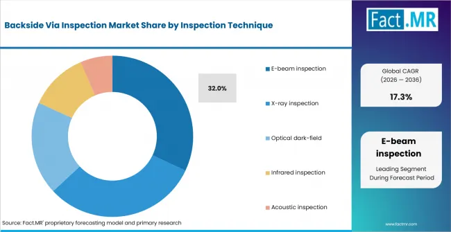
Backside Via Inspection Market Analysis By Inspection Technique | Source: Fact.MR
Electron-beam inspection provides the spatial resolution and voltage-contrast sensitivity needed to find tiny via opens, residue or landing failures. It can detect electrical behavior that is not visible as a large geometric defect. X-ray inspection offers three-dimensional coverage, but the smallest nano-TSV defects challenge its resolution and throughput. Intel PowerVia production and TSMC A16 Super Power Rail roadmaps convert backside-via inspection from TEM-based R&D sampling to in-line e-beam/X-ray flows (2024-2026 inflection). Buyers therefore tend to treat e-beam inspection as the practical choice when qualification must balance process capability, repeatability and production economics.
Why do Via voids lead Defect Type?
Via voids are projected to account for 46.0% share in 2026.
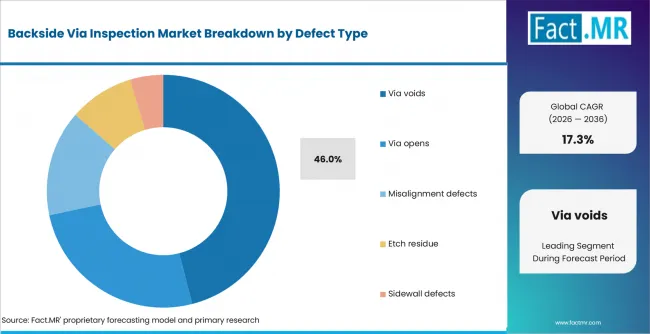
Backside Via Inspection Market Analysis By Defect Type | Source: Fact.MR
A via void reduces conductive cross-section and can create a latent resistance or reliability failure after metallization. Because the feature is buried, early detection prevents a weak connection from escaping into final backside routing. A complete via open is easier to classify electrically, while partial voids require more sensitive imaging and can be harder to screen. From hybrid-bond/TSV failure-analysis practice, adapted to backside vias: voids and delamination at the wafer-bond interface (C-SAM screens; voids appear as white specs in acoustic images); via-profile anomalies (under-etch, not-through vias); mis-landing (overlay error); Cu/liner voids in via fill. FA sequencing - non-destructive C-SAM/X-ray first, then X-ray CT for 3D localization, then FIB/TEM confirmation - is the documented workflow. Buyers therefore tend to treat via voids as the practical choice when qualification must balance process capability, repeatability and production economics.
Why does <50 nm lead Via Dimension?
<50 nm is projected to account for 42.1% share in 2026.
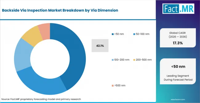
Backside Via Inspection Market Analysis By Via Dimension | Source: Fact.MR
Dimensions below 50 nanometers correspond to nano-TSVs aimed at buried power rails and advanced-node backside contacts. At that scale, a few nanometers of residue, taper or mis-landing consume a large share of the available cross-section. The 50-100 nanometer class provides more inspection and fill margin and can be served by a wider set of modalities. E-beam voltage contrast localizes opens/shorts in buried via chains at 1-3 nm sensitivity class (KLA eSL10; industry comparison data) - essential because backside vias are unreachable by probes until backside metal exists.
Why does Inline sampling lead Inspection Mode?
Inline sampling is projected to account for 43.7% share in 2026.
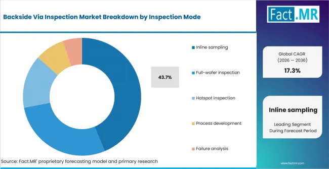
Backside Via Inspection Market Analysis By Inspection Mode | Source: Fact.MR
Inline sampling balances electron-beam sensitivity against the scan-time penalty of full-wafer coverage. It allows hotspots and process signatures to be monitored frequently while escalating suspect sites to deeper review. Full-wafer inspection maximizes coverage but is difficult to justify at e-beam acquisition speeds for every production wafer. NTSVs must land within about 10 nm of frontside targets (Cadence/IEDM). This is an order of magnitude tighter than any packaging overlay - inspection must measure buried landing accuracy through silicon, rather than surface placement alone.
Why do Foundries lead End User?
Foundries are projected to account for 29.0% share in 2026.
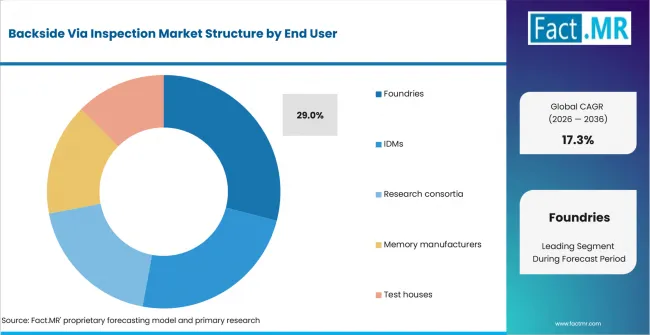
Backside Via Inspection Market Analysis By End User | Source: Fact.MR
Foundries need a scalable inspection strategy because backside-via layouts and buried targets vary by customer design. They also must link inspection results to frontside process history and downstream metallization yield. IDMs can use more design-specific recipes, while foundries benefit more from adaptable hotspot and voltage-contrast methods. Backside power delivery with ~320nm deep nTSVs landing on the BPRs at a tight pitch of 200nm with tight overlay control, processed after bonding the device wafer to a carrier and backside thinning - verified by TEM showing scaled FinFETs connected to both backside and frontside with no device degradation.
What is accelerating Backside Via Inspection Market adoption, and what is holding it back?
The strongest accelerator is the structures being inspected (imec reference implementation), while the main restraint is that the smallest vias sit below the practical resolution or throughput limits of many non-destructive methods.
Drivers Impact Analysis
| DRIVER | (~) % IMPACT ON CAGR | GEOGRAPHIC RELEVANCE | IMPACT TIMELINE |
|---|---|---|---|
| The structures being inspected (imec reference implementation) | +4.8% | Global leading-edge fabs | Medium term (2-4 years) |
| Alignment-inspection budget | +4.0% | Global leading-edge fabs | Medium term (2-4 years) |
| Defect classes | +3.3% | Global leading-edge fabs | Medium term (2-4 years) |
| X-ray capability trajectory | +2.6% | Global leading-edge fabs | Medium term (2-4 years) |
Source: Fact.MR analysis. Updated Jul 23, 2026
- The structures being inspected (imec reference implementation): Backside power delivery with ~320nm deep nTSVs landing on the BPRs at a tight pitch of 200nm with tight overlay control, processed after bonding the device wafer to a carrier and backside thinning - verified by TEM showing scaled FinFETs connected to both backside and frontside with no device degradation.
- Alignment-inspection budget: NTSVs must land within about 10 nm of frontside targets (Cadence/IEDM). This is an order of magnitude tighter than any packaging overlay - inspection must measure buried landing accuracy through silicon, rather than surface placement alone.
- Defect classes: From hybrid-bond/TSV failure-analysis practice, adapted to backside vias: voids and delamination at the wafer-bond interface (C-SAM screens; voids appear as white specs in acoustic images); via-profile anomalies (under-etch, not-through vias); mis-landing (overlay error); Cu/liner voids in via fill.
- X-ray capability trajectory: Sub-micron 3D X-ray (nano-CT/laminography, <100 nm voxels demonstrated on HBM micro-bumps and 1.5 µm hybrid bonds) is explicitly projected to grow in importance following ongoing developments with... backside power delivery (Excillum, IEEE Hybrid Bonding Symposium) - backside vias at 200 nm pitch are the next application of this resolution class.
Opportunity Impact Analysis
| OPPORTUNITY | (~) % IMPACT ON CAGR | GEOGRAPHIC RELEVANCE | IMPACT TIMELINE |
|---|---|---|---|
| From R&D metrology to HVM inspection | +2.9% | Global leading-edge fabs | Short term (<=2 years) |
| Through-silicon optical/IR inspection | +2.2% | Global leading-edge fabs | Medium term (2-4 years) |
| Voltage-contrast screening at the via layer | +1.7% | Global leading-edge fabs | Medium term (2-4 years) |
Source: Fact.MR analysis. Updated Jul 23, 2026
- From R&D metrology to HVM inspection: Intel PowerVia production and TSMC A16 Super Power Rail roadmaps convert backside-via inspection from TEM-based R&D sampling to in-line e-beam/X-ray flows (2024-2026 inflection).
- Voltage-contrast screening at the via layer: Inspecting the nTSV pattern immediately post-etch/post-fill for opens before backside metallization commits the wafer.
Restraints Impact Analysis
| RESTRAINT | (~) % IMPACT ON CAGR | GEOGRAPHIC RELEVANCE | IMPACT TIMELINE |
|---|---|---|---|
| Primary qualification constraint | -2.6% | Global leading-edge fabs | Medium term (2-4 years) |
| Alignment and registration risk | -2.1% | Global leading-edge fabs | Medium term (2-4 years) |
| Buried-defect escape | -1.6% | Global leading-edge fabs | Medium term (2-4 years) |
Source: Fact.MR analysis. Updated Jul 23, 2026
- Primary qualification constraint: The smallest vias sit below the practical resolution or throughput limits of many non-destructive methods.
- Alignment and registration risk: Backside power delivery with ~320nm deep nTSVs landing on the BPRs at a tight pitch of 200nm with tight overlay control, processed after bonding the device wafer to a carrier and backside thinning - verified by TEM showing scaled FinFETs connected to both backside and frontside with no device degradation.
- Buried-defect escape: From hybrid-bond/TSV failure-analysis practice, adapted to backside vias: voids and delamination at the wafer-bond interface (C-SAM screens; voids appear as white specs in acoustic images); via-profile anomalies (under-etch, not-through vias); mis-landing (overlay error); Cu/liner voids in via fill.
Which countries are scaling Backside Via Inspection Market fastest?
Japan is projected to record a 17.7% CAGR for Backside Via Inspection Market as semiconductor equipment, materials, inspection and memory-process expertise.
- Countries differ less by the headline CAGR than by the type of semiconductor work creating demand for the Backside Via Inspection Market.
- USA demand follows backside-power and logic-node development, while Taiwan demand reflects foundry-led integration, packaging coordination and process-control qualification.
- South Korea is shaped by high-volume memory and HBM production, while Japan contributes inspection, materials and advanced-packaging capability.
- Israel contributes process-control and advanced-logic research, whereas Ireland adds European logic-fab and production-development activity.
- Country differences reflect node mix, backside-power deployment, metrology integration, export-control exposure and qualification cycles.
The country review assesses six profiled markets within North America, Latin America, Europe, East Asia, South Asia & Oceania, and the Middle East & Africa.
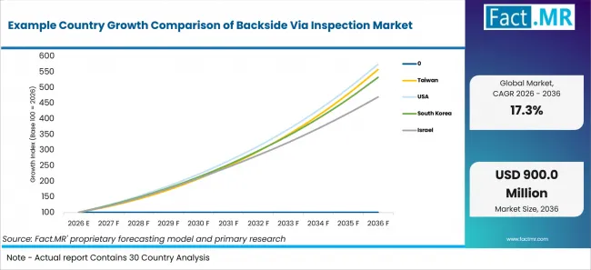
Example Country Growth Comparison Of Backside Via Inspection Market | Source: Fact.MR
| COUNTRY | CAGR, 2026 to 2036 |
|---|---|
| USA | 19.1% |
| Taiwan | 18.8% |
| South Korea | 18.2% |
| Japan | 17.7% |
| Israel | 16.8% |
| Ireland | 16.4% |
Source: Fact.MR analysis. Updated Jul 23, 2026
What is driving USA's growth through 2036?
19.1% CAGR, supported by leading-edge logic, high-performance computing, federally supported semiconductor R&D and a large domestic equipment base.
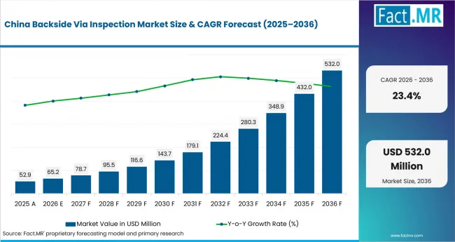
Backside Via Inspection Market Country Value Analysis | Source: Fact.MR
Intel (PowerVia - first production BSPDN, most mature backside-via inspection); KLA e-beam inspection; Onto X-ray. This environment creates a clear qualification pathway for the Backside Via Inspection Market because buyers must solve the problem of detecting opens, voids, mis-landing and sidewall defects in nano-scale vias etched from the wafer backside to buried frontside targets at production scale.
What is driving Taiwan's growth through 2036?
18.8% CAGR, supported by leading foundry production, advanced packaging and a dense OSAT and substrate supply chain.
TSMC A16 Super Power Rail - direct backside contacts raise inspection difficulty (via lands on device-side contact, not rail). This environment creates a clear qualification pathway for the Backside Via Inspection Market because buyers must solve the problem of detecting opens, voids, mis-landing and sidewall defects in nano-scale vias etched from the wafer backside to buried frontside targets at production scale.
What is driving South Korea's growth through 2036?
18.2% CAGR, supported by high-volume memory, HBM and vertically integrated semiconductor manufacturing.
Samsung BSPDN roadmap. This environment creates a clear qualification pathway for the Backside Via Inspection Market because buyers must solve the problem of detecting opens, voids, mis-landing and sidewall defects in nano-scale vias etched from the wafer backside to buried frontside targets at production scale.
What is driving Japan's growth through 2036?
17.7% CAGR, supported by semiconductor equipment, materials, inspection and memory-process expertise.
Hitachi High-Tech CD-SEM; TEL etch/bond ecosystem. This environment creates a clear qualification pathway for the Backside Via Inspection Market because buyers must solve the problem of detecting opens, voids, mis-landing and sidewall defects in nano-scale vias etched from the wafer backside to buried frontside targets at production scale.
What is driving Israel's growth through 2036?
16.8% CAGR, supported by advanced logic manufacturing and process-control R&D.
Israel combines advanced logic manufacturing and process-control R&D with a 10.4% share of 2026 demand across the six profiled countries. Backside power delivery with ~320nm deep nTSVs landing on the BPRs at a tight pitch of 200nm with tight overlay control, processed after bonding the device wafer to a carrier and backside thinning - verified by TEM showing scaled FinFETs connected to both backside and frontside with no device degradation. The commercial link is the need to solve the problem of detecting opens, voids, mis-landing and sidewall defects in nano-scale vias etched from the wafer backside to buried frontside targets as capacity and process complexity increase.
What is driving Ireland's growth through 2036?
16.4% CAGR, shaped by Ireland's European logic-fab operations and process-development activity.
Ireland combines European logic manufacturing and process-development investment with a 7.7% share of 2026 demand across the six profiled countries. NTSVs must land within about 10 nm of frontside targets (Cadence/IEDM). The commercial link is the need to solve the problem of detecting opens, voids, mis-landing and sidewall defects in nano-scale vias etched from the wafer backside to buried frontside targets as capacity and process complexity increase.
Who leads the Backside Via Inspection Market?
Applied Materials and KLA lead the competitive landscape, followed by Hitachi High-Tech and Zeiss as the next tier of challengers.
Applied Materials participates through deposition, etch, materials engineering and integrated process modules. Its relevance rests on the ability to help detect opens, voids, mis-landing and sidewall defects in nanoscale vias etched from the wafer backside to buried frontside targets. KLA participates through optical and electron-beam inspection, metrology and wider process-control systems. Its ESL10 e-beam platform uses voltage contrast at the 1–3 nm class for advanced logic structures below the surface. Hitachi High-Tech provides CD-SEM and semiconductor inspection systems for finding defects in nanoscale backside vias. ZEISS contributes X-ray microscopy, electron imaging and semiconductor metrology for inspecting internal structures that surface methods may not fully capture.
Onto Innovation has a specialized role in advanced packaging inspection, overlay and process-control metrology. Its X-ray and overlay capabilities extend to bonded backside stacks, drawing on through-glass via and through-silicon via inspection experience. ASML, through HMI, focuses on electron-beam inspection and computational process control, especially where custom integration and service coverage shape equipment qualification.
Competition is expected to focus on repeatable process performance, integration with nearby modules, installed-base service and proven defect-detection capability. Semiconductor manufacturers are expected to compare inspection accuracy, defect prevention, throughput, recipe stability and the completeness of the delivered process cell.
Which companies are the key providers?
Key companies include Applied Materials; KLA; Hitachi High-Tech; Zeiss; Onto Innovation; ASML (HMI).
- Applied Materials
- KLA
- Hitachi High-Tech
- Zeiss
- Onto Innovation
- ASML (HMI)
Bibliography
- Imec. (2025). A path to high-density front- and backside wafer connectivity.
- Hållstedt, J. (2024). Metrology for hybrid bonds, microbumps and TSVs in advanced packaging—Are X-ray methods up to the task? IEEE Electronics Packaging Society, First IEEE Hybrid Bonding Symposium.
- KLA Corporation. (2020, July 20). KLA introduces breakthrough electron-beam defect inspection system.
- ASM International. (2026, May). Electronic Device Failure Analysis, 28(2): Inspection and metrology challenges in hybrid bonding.
This Report Addresses
- The report provides strategic intelligence on Backside Via Inspection Market across Inspection Technique and Defect Type choices that shape purchasing decisions.
- Segment analysis covers E-beam inspection as the share leader within the 2026 market structure.
- Regional analysis compares Taiwan and USA with South Korea and Israel, then contrasts Japan and Ireland through their roles in backside-power and advanced-packaging supply chains.
- Competitive analysis profiles Applied Materials and KLA alongside Hitachi High-Tech and Zeiss, followed by additional active providers.
- Use-case assessment covers the categories and applications that shape demand in the Backside Via Inspection Market across the forecast period.
What does the Backside Via Inspection Market cover?
The market covers equipment and process systems configured to address the challenge of detecting opens, voids, mis-landing and sidewall defects in nano-scale vias etched from the wafer backside to buried frontside targets.
Backside via inspection covers defect detection and dimensional verification of nano-through-silicon vias (nTSVs) etched from the wafer backside into the front-end stack - landing on buried power rails or M1 pads - plus the bonded-carrier interfaces they pass through. Target structures: ~320 nm-deep nTSVs at 200 nm pitch, etched through <10 µm residual silicon.
Commercial value covers backside-via inspection optics, wafer and carrier handling, defect classification, process-control software and integration services. Finished devices, package value and unrelated front-end or packaging equipment are excluded.
What is included in the scope?
The scope includes systems used by foundries and the other end-user groups listed in the segmentation.
The market is segmented by Inspection Technique, including E-beam inspection, X-ray inspection, Optical dark-field, Infrared inspection, Acoustic inspection; Defect Type, including Via voids, Via opens, Misalignment defects, Etch residue, Sidewall defects; Via Dimension, including <50 nm, 50-100 nm, 100-200 nm, 200-500 nm, >500 nm; Inspection Mode, including Inline sampling, Full-wafer inspection, Hotspot inspection, Process development, Failure analysis; End User, including Foundries, IDMs, Research consortia, Memory manufacturers, Test houses.
Carrier handling, alignment, metrology, cleaning, defect-classification and process-control modules are included only when supplied with the configured backside-via inspection system.
What is excluded from the scope?
The scope excludes unrelated semiconductor equipment, standalone materials and components sold independently of the configured system.
It also excludes facility construction, cleanroom infrastructure, the value of processed wafers or packages, and adjacent process steps that are not part of the defined equipment category.
How Was the Analysis Built?
Fact.MR is of the opinion that this assessment combines structured market analysis with a review of public information and industry evidence relevant to the market.
- Market Assessment: The analysis considers demand patterns, supply conditions, segment mix, country activity, company participation, and adoption trends.
- Evidence Review: Public company disclosures, government and regulatory publications, trade information, technical literature, and industry records inform the assessment.
- Validation and Updates: Findings are cross-checked against available market indicators and reviewed when material market developments emerge.
Segmentation
What is the report's scope and coverage?
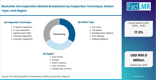
Backside Via Inspection Market Breakdown By Inspection Technique, Defect Type, And Region | Source: Fact.MR
| Attribute | Details |
|---|---|
| Quantitative Units | USD 182.0 million in 2026 to USD 900.0 million by 2036 at a 17.3% CAGR |
| Market Definition | Backside via inspection covers defect detection and dimensional verification of nano-through-silicon vias (nTSVs) etched from the wafer backside into the front-end stack - landing on buried power rails or M1 pads - plus the bonded-carrier interfaces they pass through. Target structures: ~320 nm-deep nTSVs at 200 nm pitch, etched through <10 µm residual silicon. |
| Inspection Technique | E-beam inspection; X-ray inspection; Optical dark-field; Infrared inspection; Acoustic inspection |
| Defect Type | Via voids; Via opens; Misalignment defects; Etch residue; Sidewall defects |
| Via Dimension | <50 nm; 50-100 nm; 100-200 nm; 200-500 nm; >500 nm |
| Inspection Mode | Inline sampling; Full-wafer inspection; Hotspot inspection; Process development; Failure analysis |
| End User | Foundries; IDMs; Research consortia; Memory manufacturers; Test houses |
| Regions Covered | North America; Latin America; Europe; East Asia; South Asia & Oceania; Middle East & Africa |
| Countries Covered | Taiwan; USA; South Korea; Israel; Japan; Ireland |
| Key Companies Profiled | Applied Materials; KLA; Hitachi High-Tech; Zeiss; Onto Innovation; ASML (HMI) |
| Forecast Period | 2026 to 2036 |
| Approach | Hybrid top-down and bottom-up approach using demand indicators across Inspection Technique; Defect Type; Via Dimension; Inspection Mode; End User; country-level growth; company participation and adoption trends |
Source: Fact.MR analysis. Updated Jul 23, 2026
How is the market segmented?
-
By Inspection Technique:
- E-beam inspection
- X-ray inspection
- Optical dark-field
- Infrared inspection
- Acoustic inspection
-
By Defect Type:
- Via voids
- Via opens
- Misalignment defects
- Etch residue
- Sidewall defects
-
By Via Dimension:
- <50 nm
- 50-100 nm
- 100-200 nm
- 200-500 nm
- >500 nm
-
By Inspection Mode:
- Inline sampling
- Full-wafer inspection
- Hotspot inspection
- Process development
- Failure analysis
-
By End User:
- Foundries
- IDMs
- Research consortia
- Memory manufacturers
- Test houses
-
By Region:
- North America
- Latin AmericaEurope
- South Asia & Oceania
- Middle East & Africa
Frequently Asked Questions
Which Inspection Technique leads the Backside Via Inspection Market?
Which Defect Type leads the Backside Via Inspection Market?
Which Via Dimension leads the Backside Via Inspection Market?
Which Inspection Mode leads the Backside Via Inspection Market?
Which End User leads the Backside Via Inspection Market?
What CAGR is projected for USA in the Backside Via Inspection Market?
What CAGR is projected for Taiwan in the Backside Via Inspection Market?
What CAGR is projected for South Korea in the Backside Via Inspection Market?
What CAGR is projected for Japan in the Backside Via Inspection Market?
What CAGR is projected for Israel in the Backside Via Inspection Market?
What CAGR is projected for Ireland in the Backside Via Inspection Market?
What is the primary driver of the Backside Via Inspection Market?
What is the main restraint in the Backside Via Inspection Market?
Who worked on this report


Preview the report firsthand - request a free sample
Free SampleGet the brochure for pricing and purchase details
Download PDF