- Market Value (2025): USD 2.1 Bn
- Estimated Value (2026): USD 2.4 Bn
- Forecast Value (2036): USD 10.7 Bn
- CAGR (2026-2036): 16.1%
What is the Heterogeneous Chip Tools Market forecast to be worth by 2036?
USD 2.4 billion in 2026 to USD 10.7 billion by 2036 at a 16.1% CAGR.
- The Heterogeneous Chip Tools Market reached USD 2.1 billion in 2025.
- Demand is projected to increase from USD 2.4 billion in 2026 to USD 10.7 billion by 2036.
- The market is forecast to record 16.1% CAGR from 2026 to 2036, supported by chiplet partitioning, 2.5D interposer flows and AI accelerator design complexity.
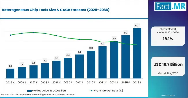
Heterogeneous Chip Tools Value Analysis | Source: Fact.MR
What are the defining numbers behind Heterogeneous Chip Tools Market growth?
An absolute opportunity of USD 8.3 billion is expected between 2026 and 2036.
- Demand Drivers in the Market
- AI accelerator architects need earlier chiplet partitioning because memory bandwidth and package area now shape architecture choices before layout begins.
- Package engineering teams need co-design environments as 2.5D interposers and silicon bridges bring substrate planning closer to front-end design.
- Interface teams need formal die-to-die verification because UCIe and proprietary protocols define link behavior before signoff.
- Back-end engineering teams need thermal, power and signal analysis as 2.5D and 3D packages concentrate heat near dense interconnects.
- Key Segments Analyzed
- By Tool Domain: Chiplet architecture and partitioning is expected to hold 25.0% share in 2026 because die partitioning sets the physical and commercial boundary for later tool decisions.
- By Integration Platform: 2.5D interposer is projected to account for 30.0% share in 2026, supported by AI packages that place logic near HBM and networking dies.
- By Design Target: AI and HPC is anticipated to capture 34.0% share in 2026 owing to accelerator programs that require dense memory links and higher package review depth.
- By Automation Level: Rule-based EDA is estimated to represent 39.0% share in 2026, driven by foundry-aligned checks and repeatable signoff flows.
- Analyst Opinion at Fact.MR
- Shambhu Nath Jha, Principal Consultant at Fact.MR, states, “Heterogeneous integration is making package context a design decision. Teams are no longer treating chiplets, interposers and thermal behavior as late-stage handoffs. Tool vendors are expected to gain when they combine architecture planning, interface validation and multiphysics signoff in one auditable flow.”
- Strategic Implications
- EDA vendors should connect partitioning, package planning and signoff evidence so design teams trace decisions across the full multi-die flow.
- Foundry ecosystem partners should publish clearer enablement routes for 2.5D and 3D packages so smaller design teams reach tapeout readiness faster.
- Chiplet IP providers should align interface models with UCIe compliance requirements and package-aware signal checks.
- System companies should include thermal and power analysis earlier in architecture planning to reduce late design rework.
Japan is projected to record 18.8% CAGR through 2036, driven by public AI and semiconductor support. Taiwan is expected to post 15.1% CAGR due to advanced packaging investment and local testing capacity. South Korea is anticipated to advance at 13.9% CAGR, supported by HBM and AI-server semiconductor momentum. The UK is forecast to reach 12.4% CAGR through AI hardware programs, while the USA is estimated to record 11.3% CAGR through CHIPS advanced packaging awards.
How does the Heterogeneous Chip Tools Market break down by segment?
2.5D interposer leads Integration Platform at 30.0%; AI and HPC leads Design Target at 34.0%.
Which Tool Domain dominates?
Chiplet architecture and partitioning is expected to hold 25.0% share in 2026.
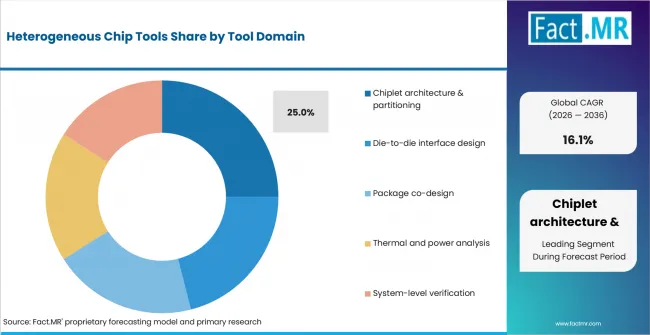
Heterogeneous Chip Tools Analysis By Tool Domain | Source: Fact.MR
Chiplet architecture and partitioning is expected to lead tool domain spending because the first design split controls interface, memory and package choices. Die-to-die interface design follows where UCIe and proprietary links require consistent electrical validation. Cadence expanded its collaboration with TSMC in April 2025 to support TSMC 3DFabric design and packaging. Its Integrity 3D-IC Platform adds AI-powered partitioning and optimization, global resource optimization, and multiphysics convergence analysis across timing, power/IR and thermal domains.
What leads the Integration Platform segment?
2.5D interposer is projected to account for 30.0% share in 2026.
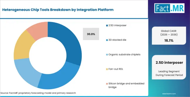
Heterogeneous Chip Tools Analysis By Integration Platform | Source: Fact.MR
2.5D interposer is projected to account for 30.0% share because AI accelerators and HPC processors need high-bandwidth links between logic and memory. 3D stacked die follows where vertical placement supports compact packages. Synopsys reported in April 2026 that its 3DIC Compiler platform delivered productivity improvement for TSMC’s CoWoS technology at 5.5× reticle interposer sizes, enabling efficient 3D multi-die designs.
How does Design Target shape demand?
AI and HPC is anticipated to capture 34.0% share in 2026.
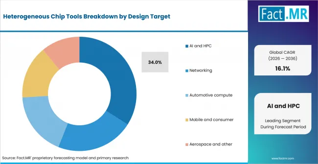
Heterogeneous Chip Tools Analysis By Design Target | Source: Fact.MR
AI and HPC is anticipated to capture 34.0% share because accelerator packages place high pressure on memory bandwidth and heat movement. Networking designs follow as switch ASICs and optical links create signal-integrity needs. Automotive compute uses heterogeneous integration where reliability and qualification evidence carry commercial weight.
What supports Rule-based EDA within Automation Level?
Rule-based EDA is estimated to represent 39.0% share in 2026.
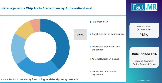
Heterogeneous Chip Tools Analysis By Automation Level | Source: Fact.MR
Rule-based EDA is estimated to represent 39.0% share because foundry and packaging rules remain the practical gate for customer acceptance. Constraint-driven optimization follows when routing and thermal limits need repeatable checks. Siemens expanded its 3D IC design portfolio in June 2025 with a new Innovator3D IC solution suite and Calibre 3DStress. Innovator3D IC supports planning and implementation of heterogeneous 2.5D/3D IC designs, while Calibre 3DStress provides thermo-mechanical analysis of chip and package interactions.
What is accelerating Heterogeneous Chip Tools Market adoption, and what is holding it back?
Chiplet complexity drives it; qualification burden restrains it.
Drivers Impact Analysis
| Driver | (~) % Impact on CAGR | Geographic Relevance | Impact Timeline |
|---|---|---|---|
| AI accelerator and HBM package complexity | +2.0% | USA, Taiwan, South Korea, Japan | Short term (<= 2 years) |
| 2.5D and 3D package co-design need | +1.6% | East Asia, North America | Medium term (2-4 years) |
| UCIe and die-to-die interface standardization | +1.2% | Global | Medium term (2-4 years) |
| Thermal and power signoff pressure | +0.9% | USA, UK, Japan | Long term (>= 4 years) |
- AI accelerator and HBM package complexity: AI processors require wider memory interfaces, shorter die-to-die connections, and increasingly complex package architectures. This creates demand for tools that help design teams evaluate chiplet partitioning, memory placement, and interconnect choices before detailed package implementation begins.
- 2.5D and 3D package co-design need: Advanced packaging requires coordinated analysis of die placement, substrates, interposers, routing constraints, and signoff requirements. Software platforms that connect package architecture with electrical, mechanical, and manufacturing considerations can reduce redesign work as 2.5D and 3D integration expands.
- UCIe and die-to-die interface standardization: Standardized die-to-die interfaces support more structured chiplet integration across heterogeneous packages. Design teams need tools for link-margin analysis, interface compliance, signal integrity, and interoperability assessment as standardized chiplet architectures become more widely adopted.
- Thermal and power signoff pressure: Dense multi-die packages create tightly coupled thermal, power, mechanical, and electrical challenges. Multiphysics analysis is therefore becoming increasingly important in package-aware design flows, particularly where high-power accelerators and stacked memory must operate within demanding temperature and reliability limits.
Opportunity Impact Analysis
| Opportunity | (~) % Impact on CAGR | Geographic Relevance | Impact Timeline |
|---|---|---|---|
| AI-assisted architecture exploration | +1.4% | Global | Medium term (2-4 years) |
| Silicon bridge and embedded bridge validation | +1.1% | USA, Taiwan | Short term (<= 2 years) |
| Package-to-board co-analysis | +0.8% | North America, East Asia, UK | Long term (>= 4 years) |
- AI-assisted architecture exploration: Early package design involves numerous placement, routing, thermal, and power trade-offs. AI-assisted tools can help engineering teams compare chiplet configurations more quickly while retaining a traceable review path for architecture decisions.
- Silicon bridge and embedded bridge validation: Advanced bridge technologies create opportunities for earlier pre-silicon analysis of die-to-die links and interface behavior. Validation tools that support emerging bridge architectures can help teams evaluate signal integrity, interoperability, and compliance before physical package builds.
- Package-to-board co-analysis: Package and PCB decisions increasingly need to be reviewed together because interconnect, routing, thermal, and mechanical constraints extend beyond the package boundary. Tool vendors can gain when they provide coordinated evidence across package, board, and assembly design flows.
Restraints Impact Analysis
| Restraint | (~) % Impact on CAGR | Geographic Relevance | Impact Timeline |
|---|---|---|---|
| Long qualification cycles | -0.8% | Global | Short term (<= 2 years) |
| Limited package-aware design skills | -0.6% | USA, UK, Japan | Medium term (2-4 years) |
| Tool-chain integration burden | -0.5% | Global | Medium term (2-4 years) |
- Long qualification cycles: Multi-die design flows require coordinated evidence across IC design, package layout, verification, and signoff. Vendors with validated reference flows and reusable methodologies can help shorten qualification work, particularly for customers running repeated heterogeneous-integration programs.
- Limited package-aware design skills: Heterogeneous integration requires engineers who understand chip architecture, interconnect behavior, thermal constraints, and package design together. Near-term adoption can therefore remain concentrated among teams with established advanced-packaging expertise and mature design-flow capabilities.
- Tool-chain integration burden: Engineering teams often combine IC design, package planning, simulation, and system-analysis tools from multiple vendors. Inconsistent data exchange and workflow handoffs can increase integration effort, while cleaner interfaces and standardized exchange formats can simplify management across several chiplet programs.
Which countries are scaling the Heterogeneous Chip Tools Market through 2036?
- The country comparison spans 7.53 percentage points and forms three practical growth bands across the forecast period.
- Japan remains 3.73 percentage points above Taiwan through public AI and semiconductor support.
- Taiwan remains 1.14 percentage points above South Korea as advanced packaging and testing capacity expands.
- South Korea remains 1.50 percentage points above the UK through HBM and AI-server semiconductor momentum.
- The UK remains 1.16 percentage points above the USA as AI hardware support widens design-led semiconductor activity.
- The USA closes the displayed range through CHIPS R&D awards and domestic advanced packaging pilot activity.
Comparable CAGRs create different entry conditions due to packaging capacity, public semiconductor policy and foundry ecosystem depth. Full report coverage includes North America, Latin America, Western Europe, Eastern Europe, East Asia, South Asia and Pacific, and Middle East and Africa.
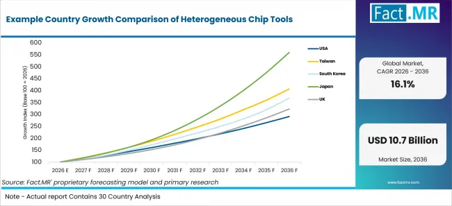
Example Country Growth Comparison Of Heterogeneous Chip Tools | Source: Fact.MR
| Country | CAGR |
|---|---|
| Japan | 18.8% |
| Taiwan | 15.1% |
| South Korea | 13.9% |
| UK | 12.4% |
| USA | 11.3% |
What supports Japan adoption?
18.8% CAGR through 2036, driven by AI and semiconductor industrial policy.
Japan’s chip design ecosystem is anchored by public support for next-generation semiconductors and domestic AI hardware. Japan is projected to record 18.8% CAGR through 2036. METI states that the AI and Semiconductor Industrial Base Strengthening Framework, formulated under Japan’s November 2024 economic measures, provides more than JPY 10 trillion in public support for the AI and semiconductor sectors over the seven years through FY2030. Rapidus-related design-environment work raises local need for partitioning, package co-design and verification tools that shorten the route from architecture to pilot manufacturing.
How is Taiwan scaling heterogeneous chip tools demand?
15.1% CAGR through 2036, led by advanced packaging capacity expansion.
Taiwan’s design and packaging ecosystem gives tool vendors a close link to foundry and OSAT customers. Taiwan is expected to post 15.1% CAGR through 2036 as DGBAS reported that Taiwan’s manufacturing sector grew 26.75% year over year in 2025Q4, mainly due to output expansion in semiconductors, computers, electronics and optical products. Advanced packaging investment is expected to keep package co-design and die-to-die verification close to customer qualification flows.
What supports South Korea’s outlook?
13.9% CAGR through 2036, supported by memory, AI server and packaging demand.
South Korea’s memory base creates a natural route into HBM-linked accelerator packages. South Korea is anticipated to advance at 13.9% CAGR through 2036 after MOTIR and MSIT reported Korea’s ICT exports reached USD 264.3 billion in 2025. Memory suppliers and AI server customers need co-design tools that connect chiplet partitioning, interface checks and thermal limits around high-bandwidth packages.
What underpins the UK’s growth?
12.4% CAGR through 2036, backed by AI hardware and chip design capability.
The UK market is shaped by design-led semiconductor firms and emerging AI hardware programs. The UK is forecast to reach 12.4% CAGR through 2036 after the UK government announced its AI Hardware Plan in June 2026, backed by over GBP 1.1 billion in targeted public and private investment. Design teams in this environment need architecture exploration and package validation tools that help convert research hardware into manufacturable chip systems.
How does the USA perform?
11.3% CAGR through 2036, driven by advanced packaging awards and domestic design infrastructure.
The USA has a deep EDA base and a policy route toward domestic advanced packaging. The USA is estimated to record 11.3% CAGR through 2036 after the U.S. Department of Commerce announced in January 2025 that the CHIPS National Advanced Packaging Manufacturing Program had finalized USD 1.4 billion in awards to support advanced semiconductor packaging. Design and packaging teams need certified flows that connect substrates, interposers and system-level verification with pilot-line readiness.
Who leads the Heterogeneous Chip Tools Market?
Cadence and Synopsys provide direct 3D-IC design-flow coverage, while Siemens EDA and Keysight Technologies provide package-analysis and interface-validation capabilities.
Cadence and Synopsys provide capabilities spanning chiplet planning, advanced-package implementation and foundry-enabled 3D-IC design flows. Cadence connects its Integrity 3D-IC Platform with TSMC 3DFabric enablement, integrating system planning, chip and package implementation, and multiphysics analysis. Synopsys 3DIC Compiler supports advanced multi-die design, including TSMC CoWoS at 5.5× reticle interposer sizes, and integrates thermal, power-integrity and signal-integrity analysis. Both companies extend their positions through certified foundry flows and integrated workflows spanning die, package and system-level design.
Siemens EDA competes through Innovator3D IC and Calibre 3DStress. Innovator3D IC covers design planning, heterogeneous integration, substrate and interposer implementation, and interface compliance analysis, while Calibre 3DStress provides thermo-mechanical stress analysis for 3D-IC and advanced-packaging designs. Ansys, now part of Synopsys, adds thermal, electromagnetic, power-integrity and broader multiphysics analysis capabilities. Keysight Technologies supports chiplet pre-silicon validation through Chiplet PHY Designer, including UCIe-based workflows and support for Intel Foundry EMIB-T technology.
Which companies are the key providers?
Key companies include Cadence, Synopsys (including Ansys), Siemens EDA, and Keysight Technologies.
- Cadence
- Synopsys
- Siemens EDA
- Keysight Technologies
Bibliography
- Altium. (2025, September 28). Advanced technologies. Altium Designer Technical Documentation.
- ANSYS, Inc. (2025, April 29). Ansys thermal and multiphysics solutions certified for Intel 18A process and 3D-IC designs.
- Cadence Design Systems, Inc. (2025, April 24). Cadence and TSMC advance AI and 3D-IC chip design with certified design solutions for TSMC’s A16 and N2P process technologies.
- Department for Science, Innovation and Technology. (2026, June 8). A decisive shift to power British AI: New £1.1 billion plan to back chip firms, boost computing power and skills for the AI revolution. GOV.UK.
- Directorate General of Budget, Accounting and Statistics. (2026, February 13). GDP: Preliminary estimate for 2025Q4, and outlook for 2026. National Statistics, Republic of China (Taiwan).
- Keysight Technologies, Inc. (2025, April 29). Keysight EDA and Intel Foundry collaborate on EMIB-T silicon bridge technology for next-generation AI and data center solutions.
- Ministry of Trade, Industry and Resources, & Ministry of Science and ICT. (2026, January 15). ICT exports post record annual performance in 2025.
- National Institute of Standards and Technology. (2025, January 16). U.S. Department of Commerce announces $1.4 billion in final awards to support the next generation of U.S. semiconductor advanced packaging.
- SEMI. (2026, April 7). SEMI reports global semiconductor equipment billings reached $135 billion in 2025, up 15% year-on-year.
- Siemens Digital Industries Software. (2025, June 24). Siemens streamlines design and analysis of complex, heterogeneously integrated 3D ICs.
- Synopsys, Inc. (2025, July 17). Synopsys completes acquisition of Ansys.
- Synopsys, Inc. (2026, April 22). Synopsys partners with TSMC to power next-generation AI systems with silicon proven IP and certified EDA flows.
- UCIe Consortium. (2025, August 5). UCIe Consortium releases 3.0 specification with 64 GT/s performance and enhanced manageability.
This Report Addresses
- The report explains where heterogeneous chip tools are used across tool domain and integration platform. It also covers design target and automation level.
- Segment analysis identifies chiplet architecture and partitioning, 2.5D interposer, AI and HPC, and rule-based EDA as the main share leaders.
- Country analysis examines Japan, Taiwan, South Korea, the UK and the USA through policy, packaging and semiconductor-design mechanisms.
- Competitive analysis reviews Cadence, Synopsys (including Ansys), Siemens EDA, Keysight Technologies across direct and adjacent tool coverage.
- Technology assessment covers chiplet architecture, die-to-die interface design, package co-design, thermal and power analysis, and system-level verification.
What does the Heterogeneous Chip Tools Market cover?
Architecture, interface, package co-design and signoff tools used for multi-die semiconductor planning.
The market covers tools used to plan, implement and validate multi-die semiconductor systems. Related coverage links to 3D semiconductor packaging when package structures shape the software workflow.
The assessment connects to electronic design automation software where chip planning flows expand into 2.5D and 3D packages. It also relates to chiplet interconnect IP when interface qualification depends on package-aware design data.
What is included in the scope?
Heterogeneous chip tools used in 2.5D and 3D multi-die design workflows.
The scope includes software for chiplet partitioning, interface design, package co-design and verification. It includes tools used with advanced packaging process control software where design evidence connects with package-yield review. Coverage extends to GPU and HPC silicon interposers where AI packages require dense routing.
The scope includes software used around HBM CoWoS packaging capacity when teams assess memory placement. It includes workflows linked to advanced IC substrates where substrates influence routing and power delivery.
Coverage includes review for HBM silicon interposer and substrate designs where thermal behavior and signal paths are evaluated together.
What is excluded from the scope?
Standalone PCB tools and semiconductor fabrication equipment are outside the scope.
The scope excludes pure board layout tools, raw semiconductor equipment and EDA tools sold only for monolithic chip design. Adjacent PCB design software is included only when package-to-system review is part of a heterogeneous workflow.
Printed circuit board hardware and server assemblies are outside the defined boundary. The assessment links to data center and AI server printed circuit boards only where board constraints influence package-to-system analysis.
How Was the Analysis Built?
The analysis draws on 120+ sources, 35+ company portfolios, 25+ countries, and more than 20 industry interviews.
- Primary Research: Primary research includes discussions with manufacturers, service providers, technology developers, distributors, end users, and subject-matter experts. These conversations examine purchasing priorities, product adoption, operational challenges, approval requirements, competitive positioning, and the factors that influence wider market acceptance.
- Desk Research: Desk research covers government statistics, regulatory publications, company filings, trade data, technical studies, industry associations, standards, public policy, and other authoritative sources. Every source used in the analysis is documented in the bibliography.
- Market Sizing and Forecasting: Market estimates combine historical performance, demand indicators, pricing and volume trends, segment shares, company participation, country-level growth, adoption patterns, investment activity, and barriers to market expansion.
- Data Validation and Update Cycle: Findings are validated by comparing primary interviews with public data, company activity, regulatory changes, trade patterns, and industry developments. Regular updates review new product launches, capacity changes, partnerships, approvals, and shifts in commercial adoption.
What is the report’s scope and coverage?
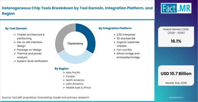
Heterogeneous Chip Tools Breakdown By Tool Domain, Integration Platform, And Region | Source: Fact.MR
| Attribute | Details |
|---|---|
| Quantitative Units | USD billion |
| Market Definition | Software used to plan, implement, analyze and verify heterogeneous multi-die chip systems, including architecture partitioning, die-to-die interface design, package co-design, thermal and power analysis, and system-level verification. |
| Tool Domain | Chiplet architecture and partitioning; Die-to-die interface design; Package co-design; Thermal and power analysis; System-level verification |
| Integration Platform | 2.5D interposer; 3D stacked die; Organic substrate chiplets; Fan-out RDL; Silicon bridge and embedded bridge |
| Design Target | AI and HPC; Networking; Automotive compute; Mobile and consumer; Aerospace and other |
| Automation Level | Rule-based EDA; Constraint-driven optimization; AI-assisted placement and exploration; Automated signoff closure; Generative architecture exploration |
| Regions Covered | North America; Latin America; Western Europe; Eastern Europe; East Asia; South Asia and Pacific; Middle East and Africa |
| Countries Covered | Japan; Taiwan; South Korea; UK; USA |
| Key Companies Profiled | Cadence; Synopsys (including Ansys); Siemens EDA; Keysight Technologies |
| Forecast Period | 2026 to 2036 |
| Approach | Hybrid top-down and bottom-up approach using tool-domain revenue, package platform mix, design target intensity, country adoption, technology certifications and provider portfolio review. |
How is the market segmented?
-
By Tool Domain
- Chiplet architecture and partitioning
- Die-to-die interface design
- Package co-design
- Thermal and power analysis
- System-level verification
-
By Integration Platform
- 2.5D interposer
- 3D stacked die
- Organic substrate chiplets
- Fan-out RDL
- Silicon bridge and embedded bridge
-
By Design Target
- AI and HPC
- Networking
- Automotive compute
- Mobile and consumer
- Aerospace and other
-
By Automation Level
- Rule-based EDA
- Constraint-driven optimization
- AI-assisted placement and exploration
- Automated signoff closure
- Generative architecture exploration
-
By Region
- North America
- Latin America
- Western Europe
- Eastern Europe
- East Asia
- South Asia and Pacific
- Middle East and Africa