- Market Value (2025): USD 3.3 Bn
- Estimated Value (2026): USD 3.8 Bn
- Forecast Value (2036): USD 18.1 Bn
- CAGR (2026-2036): 16.9%
What is the HBM Through Silicon Via TSV Technology and Equipment Market forecast to be worth by 2036?
USD 3.8 billion in 2026 to USD 18.1 billion by 2036 at 16.9% CAGR.
- The HBM Through Silicon Via TSV Technology and Equipment market reached USD 3.3 billion in 2025 as AI accelerator demand expanded qualification work for high-bandwidth memory stacks.
- Demand is projected to increase from USD 3.8 billion in 2026 to USD 18.1 billion by 2036.
- The market is forecast to record 16.9% CAGR from 2026 to 2036.
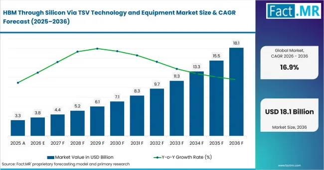
Hbm Through Silicon Via Tsv Technology And Equipment Market Value Analysis | Source: Fact.MR
What are the defining numbers behind HBM Through Silicon Via TSV Technology and Equipment Market growth?
USD 13.4 billion absolute opportunity is expected by 2036.
- Demand Drivers in the Market
- AI training and inference workloads are expected to lift demand for high-bandwidth memory chips used in accelerator and GPU server designs. The U.S. International Trade Administration reported in 2026 that South Korea's semiconductor output rose 13.2% year on year in 2025 and that annual semiconductor exports reached USD 173.4 billion in 2025, adding a clear memory-led demand signal for TSV tool qualification.
- Chiplet designs and 2.5D/3D packaging are expected to move process value toward silicon interposers, TSV formation and hybrid bonding. This makes 3D semiconductor packaging a closer buying context for TSV equipment.
- Memory manufacturers need TSV etching and wafer-level control because small process errors can reduce yield during HBM stack assembly.
- Key Segments Analyzed
- By Equipment Category: TSV Etching Equipment is expected to hold 41.0% share in 2026 because via depth and sidewall control remain central to HBM process release.
- By Application: HBM Memory Manufacturing is projected to account for 43.0% share in 2026 as stack density makes TSV reliability a purchase requirement.
- By End User: Memory Manufacturers are anticipated to capture 39.0% share in 2026 since HBM yield risk remains concentrated inside memory production flows.
- By Manufacturing Stage: Wafer Fabrication is estimated to represent 46.0% share in 2026 due to its direct role in via creation before stacking begins.
- By TSV Process Technology: Deep Reactive Ion Etching is forecast to hold 44.0% share in 2026 as deep vertical vias need stable profiles and controlled selectivity.
- Analyst Opinion at Fact.MR
- Shambhu Nath Jha, Principal Consultant at Fact.MR, states, “HBM TSV equipment is moving from a specialist packaging requirement to a purchase priority for AI memory supply. Tool suppliers that prove etch profile control and bonding readiness are expected to gain earlier qualification with memory makers and foundries.”
- Strategic Implications
- Fab engineering teams should establish TSV process-control plans before capacity negotiations begin with tool suppliers and OSAT partners.
- Equipment vendors should show how TSV process tools and queue-time hybrid bonders protect HBM yield through later process steps.
- Investors should separate direct HBM TSV exposure from broad semiconductor equipment exposure when reviewing supplier portfolios.
Taiwan leads at 18.2% CAGR through foundry scale and HBM packaging concentration. South Korea follows at 17.6% through memory manufacturing. USA records 17.1% through AI infrastructure. Japan posts 16.5% through materials and equipment depth. China reaches 15.8% through domestic semiconductor programs. Germany reaches 15.2% through automotive semiconductor demand. Singapore records 14.6% through specialty fabs.
How does the HBM Through Silicon Via TSV Technology and Equipment Market break down by segment?
TSV Etching Equipment is expected to lead Equipment Category at 41.0% share in 2026. HBM Memory Manufacturing is projected to lead Application at 43.0% share in 2026.
Which Equipment Category dominates?
TSV Etching Equipment is projected to account for 41.0% share in 2026.
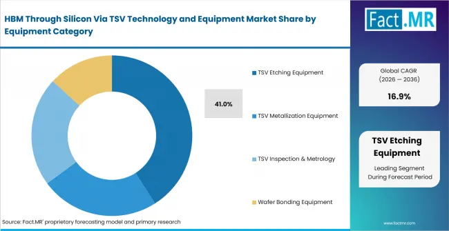
Hbm Through Silicon Via Tsv Technology And Equipment Market Analysis By Equipment Category | Source: Fact.MR
TSV Etching Equipment leads where HBM vias need deep openings with controlled sidewalls. Buyers check etch depth and profile stability before production release. 3D TSV packages create the same inspection need when via defects must be caught before bonding raises failure cost. In September 2025, Lam Research introduced VECTOR TEOS 3D for AI and HPC advanced packaging; the tool processes crack-free inter-die gapfill films above 30 microns in a single pass and delivers nearly 70% faster throughput with up to 20% better cost of ownership than Lam's prior gapfill solutions.
Why does HBM Memory Manufacturing lead Application?
HBM Memory Manufacturing is expected to hold 43.0% share in 2026.
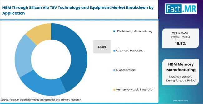
Hbm Through Silicon Via Tsv Technology And Equipment Market Analysis By Application | Source: Fact.MR
HBM manufacturing carries the largest process burden because stacked memory depends on reliable TSV formation before bonding. HBM stack inspection becomes more valuable when vias must pass alignment and defect checks before high-value wafers move downstream. In June 2026, Applied Materials introduced Nokota VMax 2 for TSV fill in 3D stacking and Producer Avila 2 PECVD for reliable stacking of 12, 16 and future high-layer-count HBM designs.
What supports Memory Manufacturers within End User?
Memory Manufacturers are anticipated to represent 39.0% share in 2026.
Memory manufacturers lead demand since HBM yield loss is costly when defects appear late in stack assembly. Foundries and OSAT providers use related tools for chiplet and interposer work. Research institutes create smaller demand for flexible qualification.
How does Wafer Fabrication shape demand?
Wafer Fabrication is estimated to account for 46.0% share in 2026.
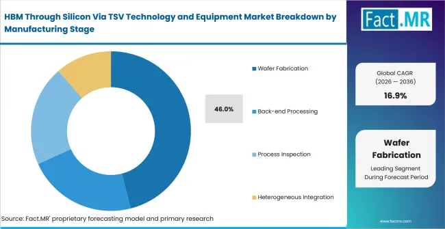
Hbm Through Silicon Via Tsv Technology And Equipment Market Analysis By Manufacturing Stage | Source: Fact.MR
Wafer Fabrication leads at the point where TSV structures must be formed and checked before thinning or stacking begins. Equipment selection must account for via landing and wafer backside quality. This makes backside power metrology relevant when bonded wafers need non-destructive inspection.
Why does Deep Reactive Ion Etching lead TSV Process Technology?
Deep Reactive Ion Etching is forecast to hold 44.0% share in 2026.
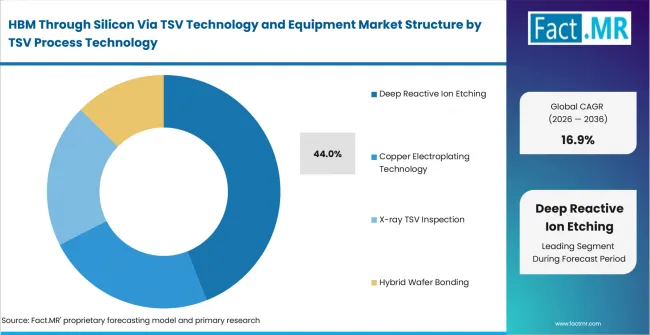
Hbm Through Silicon Via Tsv Technology And Equipment Market Analysis By Tsv Process Technology | Source: Fact.MR
Deep Reactive Ion Etching leads through its role in high-aspect-ratio TSV openings that need stable depth and sidewall control. Bosch process variants and via-middle flows support different integration routes. Copper hybrid interfaces add a bonding context when via quality affects electrical contact. In September 2025, Kokusai Electric signed a joint development agreement with ASMPT for hybrid bonding and thermocompression bonding solutions for 2.5D and 3D packaging used in next-generation HPC and AI.
What is accelerating HBM Through Silicon Via TSV Technology and Equipment Market adoption, and what is holding it back?
Demand is expected to rise through AI memory scaling and TSV process qualification. Growth is likely to be limited by capital intensity, long release cycles and supply chain concentration.
Drivers Impact Analysis
| DRIVER | (~) % IMPACT ON CAGR | GEOGRAPHIC RELEVANCE | IMPACT TIMELINE |
|---|---|---|---|
| AI accelerator and HBM stack demand | High | Taiwan; South Korea; USA | Short term (<= 2 years) |
| TSV etch and via profile control | High | Taiwan; Japan; South Korea | Short term (<= 2 years) |
| Chiplet and silicon interposer use | Medium-High | USA; Taiwan; Singapore | Medium term (2-4 years) |
| Wafer-level bonding readiness | Medium | Memory and foundry clusters | Medium term (2-4 years) |
| Inspection and metrology release checks | Medium | Japan; USA; Taiwan | Long term (>= 4 years) |
Source: Fact.MR analysis. Updated Aug 10, 2026
- AI accelerator and HBM stack demand: AI compute growth is expected to raise purchase urgency for TSV tools that support high-bandwidth memory assembly.
- TSV etch and via profile control: Memory fabs place more weight on sidewall stability because small defects can reduce package yield.
- Chiplet and silicon interposer use: 2.5D/3D designs are projected to increase process value for via formation and bonding preparation.
Opportunity Impact Analysis
| OPPORTUNITY | (~) % IMPACT ON CAGR | GEOGRAPHIC RELEVANCE | IMPACT TIMELINE |
|---|---|---|---|
| Hybrid bonding readiness | Medium-High | Taiwan; South Korea; USA | Medium term (2-4 years) |
| Integrated inspection and metrology | Medium | Japan; USA; Taiwan | Medium term (2-4 years) |
| Interposer and chiplet process transfer | Medium | USA; Taiwan; Singapore | Long term (>= 4 years) |
| Service-led qualification support | Medium | China; Germany; Singapore | Long term (>= 4 years) |
Source: Fact.MR analysis. Updated Aug 10, 2026
- Hybrid bonding readiness: Tool vendors that connect via quality with bonding conditions can support faster qualification in memory packaging.
- Integrated inspection and metrology: Buyers are expected to value semiconductor defect inspection equipment that catches via defects before stacked wafers reach higher-cost steps.
- Interposer and chiplet process transfer: TSV experience can move into through-glass via interposers where routing density and packaging form factor are purchase criteria.
Restraints Impact Analysis
| RESTRAINT | (~) % IMPACT ON CAGR | GEOGRAPHIC RELEVANCE | IMPACT TIMELINE |
|---|---|---|---|
| Capital intensity and investment burden | Medium | Developing markets | Short term (<= 2 years) |
| Long qualification and customer release cycles | Medium | Memory fabs | Short term (<= 2 years) |
| Supply chain and materials concentration | Medium | Global | Medium term (2-4 years) |
| Workforce and process capability gaps | Low-Medium | Africa, Latin America | Long term (>= 4 years) |
Source: Fact.MR analysis. Updated Aug 10, 2026
- Capital intensity and investment burden: TSV equipment requires high upfront spending and long payback periods before utilization becomes clear.
- Long qualification and customer release cycles: A tool must prove repeatability across wafers and chambers before memory customers approve wider production use.
- Workforce and process capability gaps: Smaller fabs are expected to delay purchases when local teams lack deep etch, bonding and metrology experience.
Which countries are scaling the HBM Through Silicon Via TSV Technology and Equipment Market fastest?
- The country comparison spans 3.6 percentage points and forms four practical growth bands across the forecast period.
- Taiwan remains 0.6 percentage point above South Korea through foundry scale and packaging concentration.
- South Korea remains 0.5 percentage point above USA as memory manufacturing supports tool qualification.
- USA remains 0.6 percentage point above Japan through AI infrastructure and onshore fab activity.
- Japan remains 0.7 percentage point above China through equipment capability and materials depth.
- China remains 0.6 percentage point above Germany as domestic semiconductor programs keep tool support needs active.
- Germany remains 0.6 percentage point above Singapore through automotive semiconductor and industrial electronics demand.
Comparable CAGRs create different entry conditions because fab scale and engineering depth vary by country. Full report coverage includes North America and Latin America. Europe and East Asia are included. South Asia and Pacific and Middle East and Africa complete the regional coverage.
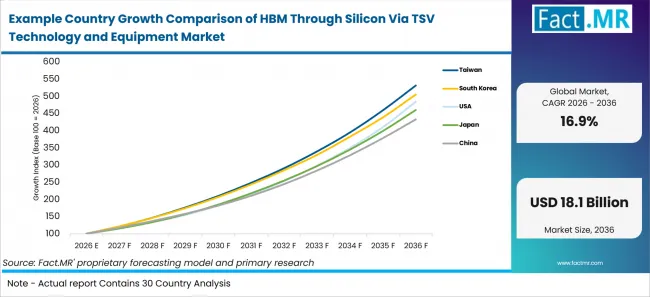
Example Country Growth Comparison Of Hbm Through Silicon Via Tsv Technology And Equipment Market | Source: Fact.MR
| Country | CAGR |
|---|---|
| Taiwan | 18.2% |
| South Korea | 17.6% |
| USA | 17.1% |
| Japan | 16.5% |
| Germany | 15.2% |
| Singapore | 14.6% |
Source: Fact.MR analysis. Updated Aug 10, 2026
What is driving Taiwan’s growth from 2026 to 2036?
18.2% CAGR, supported by foundry scale and HBM packaging concentration.
Taiwan’s growth reflects a production base where foundries and packaging partners qualify TSV tools near high-volume wafer operations. Local engineering teams can test via profile control close to commercial lines. At SEMICON Taiwan 2025, Taiwan's Ministry of Economic Affairs said its Department of Industrial Technology pavilion featured 37 advanced technologies and that related projects had attracted more than NT$2.4 billion in industry investment, while DoIT had invested nearly NT$40 billion over the prior five years in AI, HPC, silicon photonics, advanced packaging and compound semiconductors.
How is South Korea developing demand?
17.6% CAGR, driven by memory manufacturing and HBM qualification activity.
South Korea’s growth is shaped by memory production and the need to protect stack yield. Suppliers must prove chamber matching before wider deployment. Via reliability becomes a purchase condition.
What supports USA adoption?
17.1% CAGR, backed by AI infrastructure and onshore fab activity.
USA growth reflects demand from AI computing programs and onshore semiconductor activity. Buyers assess TSV equipment through process stability and release evidence before they commit to larger tool fleets.
How does Japan perform?
16.5% CAGR, led by materials depth and equipment capability.
Japan’s growth reflects semiconductor equipment expertise and materials know-how. Customers are expected to value precise etch behavior, metrology support and dependable engineering help during release trials.
What is supporting Germany’s market position?
15.2% CAGR, supported by automotive semiconductor and industrial IoT demand.
Germany’s growth is shaped by automotive electronics and industrial semiconductor requirements. Long product qualification cycles make stable process evidence more important than fast trial adoption.
What supports Singapore’s growth?
14.6% CAGR, backed by specialty fabs and regional support.
Singapore’s growth reflects a compact semiconductor cluster where specialty fabs and equipment support providers operate close to one another. Customers are likely to favor stable recipes and quick service response. In January 2025, Micron broke ground on Singapore's first HBM advanced packaging facility, backed by approximately USD 7 billion (SGD 9.5 billion) of investment, with operations scheduled for 2026 and meaningful advanced-packaging capacity expansion beginning in calendar 2027.
Who leads the HBM Through Silicon Via TSV Technology and Equipment Market?
Lam Research Corporation and Tokyo Electron Limited show the clearest process-equipment relevance. Applied Materials, Inc. supports deposition and selective etch routes. SCREEN Semiconductor Solutions Co., Ltd. and ASMPT Limited extend the field across cleaning and bonding. KLA Corporation and Onto Innovation Inc. cover inspection and process control. Hitachi High-Tech Corporation and BE Semiconductor Industries N.V. add etch and assembly equipment coverage.
Competition is concentrated among semiconductor equipment suppliers that can support long qualification cycles. Buyers compare tool stability and service depth before approving equipment for HBM process flows. Supplier relevance depends on proof across TSV formation and packaging release steps. In April 2026, Onto Innovation said its Dragonfly G5 system had achieved a second successful qualification for 2.5D AI packaging and that Dragonfly platforms were expected to grow more than 50% in 2026 compared with 2025.
Which companies are the key providers?
Key companies include Lam Research Corporation; Applied Materials, Inc. Tokyo Electron Limited; SCREEN Semiconductor Solutions Co., Ltd.; ASMPT Limited KLA Corporation, Onto Innovation Inc. and Hitachi High-Tech Corporation; and BE Semiconductor Industries N.V.
- Lam Research Corporation
- Applied Materials, Inc.
- Tokyo Electron Limited
- SCREEN Semiconductor Solutions Co., Ltd.
- ASMPT Limited
- KLA Corporation
- Onto Innovation Inc.
- Hitachi High-Tech Corporation
- BE Semiconductor Industries N.V.
Bibliography
- Applied Materials, Inc. (2026, June 15). Applied Materials unveils deposition and selective etch systems to advance 3D chip scaling.
- ASMPT Limited. (2025, August 26). ASMPT exhibits at SEMICON Taiwan 2025 - Enabling chips for AI. The title and date are correct even though the ASMPT URL oddly contains “2026.”
- BE Semiconductor Industries N.V. (2026, January 12). BE Semiconductor Industries N.V. announces trading update.
- Hitachi High-Tech Corporation. (2024, November 27). Hitachi High-Tech launches DCR Etch System 9060 Series, supporting isotropic etching of advanced 3D devices at the atomic level.
- KLA Corporation. (2026, July 28). KLA Corporation reports fiscal 2026 fourth quarter and full year results.
- KOKUSAI ELECTRIC CORPORATION. (2025, September 25). Signed a joint development agreement with ASMPT for semiconductor packaging technology.
- Lam Research Corporation. (2024, July 31). Lam Research introduces Lam Cryo™ 3.0 cryogenic etch technology to accelerate scaling of 3D NAND for the AI era.
- Onto Innovation Inc. (2026, April 16). Onto Innovation’s Dragonfly® G5 system qualified for applications in 2.5D AI packaging.
- SCREEN Holdings Co., Ltd. (2025, October 31). Acquisition of an R&D business in wafer bonding from Nikon.
- SEMI. (2026, April 7). SEMI reports global semiconductor equipment billings reached $135 billion in 2025, up 15% year-on-year.
- Tokyo Electron Limited. (2024, October 21). Cryogenic etching - Tokyo Electron’s “digital and green transformation” of semiconductor process equipment.
- Applied Materials, Inc. (2026, June 25). Applied Materials introduces new systems to accelerate DRAM and advanced packaging for AI chips.
- International Trade Administration. (2026, June 8). South Korea AI semiconductor.
- International Trade Administration. (2025, November 20). Japan - Semiconductors.
- Lam Research Corporation. (2025, September 9). Lam Research introduces VECTOR® TEOS 3D to address critical advanced packaging challenges in chipmaking.
- Micron Technology, Inc. (2025, January 8). Micron breaks ground on new HBM advanced packaging facility in Singapore.
- National Institute of Standards and Technology. (2025, January 16). U.S. Department of Commerce announces $1.4 billion in final awards to support the next generation of U.S. semiconductor advanced packaging.
- Ministry of Economic Affairs, R.O.C. (2025, September 12). MOEA showcases silicon photonics and 3D chip modules to strengthen Taiwan’s semiconductor innovation chain.
This Report Answers
- The report covers Equipment Category and Application choices that shape TSV tool demand.
- Segment analysis covers TSV Etching Equipment and HBM Memory Manufacturing as 2026 share leaders.
- Country outlook compares Taiwan and South Korea with the USA and Japan. China, Germany and Singapore complete the country view.
- Competitive analysis profiles Lam Research Corporation and Applied Materials, Inc. Tokyo Electron Limited and SCREEN Semiconductor Solutions Co., Ltd. are included with six additional suppliers.
- Process assessment covers Deep Reactive Ion Etching and Wafer Fabrication. Bonding, inspection and thermal integration complete the process view.
What does the HBM Through Silicon Via TSV Technology and Equipment Market cover?
HBM TSV technology and equipment covers tools that create and qualify through-silicon vias for HBM stacks. Etching, bonding and inspection are included when via quality affects stack reliability.
Coverage includes silicon interposers and chiplet integration when they depend on TSV process control. Automotive AI processors are included only when advanced GPU packaging requires TSV-related tools.
What is included in the scope?
The scope includes Equipment Category and Application with End User, Manufacturing Stage and TSV Process Technology. TSV etching, bonding equipment and inspection tools are covered when they support via release.
Applications include HBM manufacturing and AI accelerator packaging. GPU and HPC packaging, chiplet integration and automotive AI processors follow the same TSV qualification rule.
What is excluded from the scope?
General semiconductor equipment remains outside the scope unless it is used directly for HBM TSV formation.
Standalone packaging tools are excluded when they do not support TSV process flows. Company revenue without a clear HBM TSV connection is outside the scope.
How Was the Analysis Built?
The analysis draws on 120+ sources, 35+ company portfolios, 25+ countries, and more than 20 interviews.
- Primary Research: Interviews with manufacturers, retailers, salon operators, and experts examine purchase priorities, adoption, approval requirements, and competitive positioning.
- Desk Research: Desk research covers government statistics, regulatory publications, company filings, trade data, technical studies, industry associations, standards, and public policy.
- Market Sizing and Forecasting: Estimates combine historical performance, demand indicators, pricing, segment shares, company participation, country growth, adoption patterns, and barriers to expansion.
- Data Validation and Update Cycle: Findings are validated against public data, company activity, regulatory changes, product launches, recalls, and adoption shifts.
Segmentation
What is the report’s scope and coverage?
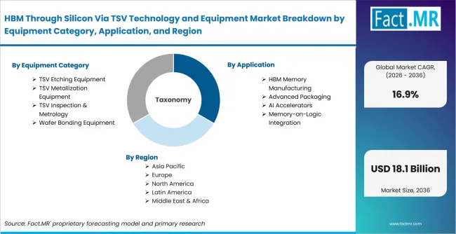
Hbm Through Silicon Via Tsv Technology And Equipment Market Breakdown By Equipment Category, Application, And Region | Source: Fact.MR
| Attribute | Details |
|---|---|
| Quantitative Units | USD billion |
| Market Definition | Equipment and process technology used to form and inspect through-silicon vias. Bonding and qualification are included when they support high-bandwidth memory stacks. |
| Equipment Category | TSV Etching Equipment; Wafer Bonding Equipment; TSV Inspection and Metrology; Deposition and Cleaning Tools; Thermal Management Equipment |
| Application | HBM Memory Manufacturing; AI Accelerator Packaging; GPU and HPC Packaging; Chiplet Integration; Automotive AI Processors |
| End User | Memory Manufacturers; Foundries; OSAT Providers; Integrated Device Manufacturers; Research Institutes |
| Manufacturing Stage | Wafer Fabrication; Wafer Thinning; Bonding and Stacking; Metrology and Inspection; Thermal Interface Integration |
| TSV Process Technology | Deep Reactive Ion Etching; Bosch Process; Via-Middle TSV; Via-Last TSV; Hybrid Bonding Readiness |
| Regions Covered | North America; Latin America; Europe; East Asia; South Asia and Pacific; Middle East and Africa |
| Countries Covered | Taiwan; South Korea; USA; Japan; China; Germany; Singapore |
| Key Companies Profiled | Lam Research Corporation; Applied Materials, Inc.; Tokyo Electron Limited; SCREEN Semiconductor Solutions Co., Ltd.; ASMPT Limited; KLA Corporation; Onto Innovation Inc.; Hitachi High-Tech Corporation; BE Semiconductor Industries N.V. |
| Forecast Period | 2026 to 2036 |
| Approach | Hybrid top-down and bottom-up approach using semiconductor equipment demand; HBM packaging requirements; TSV qualification activity; memory and foundry capacity; bonding readiness; inspection needs; country adoption patterns; company portfolio review |
Source: Fact.MR analysis. Updated Aug 10, 2026
How is the market segmented?
-
By Equipment Category
- TSV Etching Equipment
- Deep Silicon Etching Systems
- High Aspect Ratio Etchers
- TSV Metallization Equipment
- Copper Electroplating Systems
- Barrier Deposition Equipment
- TSV Inspection & Metrology
- X-ray Inspection Systems
- Optical Metrology Systems
- Wafer Bonding Equipment
- Hybrid Bonding Systems
- Temporary Wafer Bonding Systems
- TSV Etching Equipment
-
By Application
- HBM Memory Manufacturing
- HBM3E Production
- HBM4 Development
- Advanced Packaging
- Chiplet Integration
- GPU Packaging
- AI Accelerators
- High-performance Computing
- Networking Processors
- Memory-on-Logic Integration
- 2.5D-3D Packaging
- Next-generation HBM
- HBM Memory Manufacturing
-
By End User
- Memory Manufacturers
- DRAM Manufacturers
- Semiconductor Foundries
- OSAT Providers
- Advanced Packaging Companies
- GPU Manufacturers
- Logic Chip Manufacturers
- Hyperscale Infrastructure Providers
- Network Equipment Manufacturers
- Semiconductor Research Institutes
- Academic Research Centers
- Government Semiconductor Laboratories
- Memory Manufacturers
-
By Manufacturing Stage
- Wafer Fabrication
- Front-end Processing
- Advanced Process Development
- Back-end Processing
- Assembly & Packaging
- Production Packaging
- Process Inspection
- In-line Quality Control
- Failure Analysis
- Heterogeneous Integration
- Pilot Production
- Process Qualification
- Wafer Fabrication
-
By TSV Process Technology
- Deep Reactive Ion Etching
- Bosch TSV Etching Process
- High Aspect Ratio TSV Formation
- Copper Electroplating Technology
- Barrier & Seed Layer Deposition
- Chemical Vapor Deposition
- X-ray TSV Inspection
- 3D X-ray Metrology
- Optical Critical Dimension Measurement
- Hybrid Wafer Bonding
- Direct Copper-to-Copper Bonding
- Temporary Wafer Bonding Technology
- Deep Reactive Ion Etching
-
By Region
- North America
- Latin America
- Europe
- East Asia
- South Asia and Oceania
- Middle East and Africa
Frequently Asked Questions
How big is the HBM through silicon via TSV technology and equipment market in 2026?
What is the CAGR of the HBM through silicon via TSV technology and equipment market from 2026 to 2036?
Which equipment category leads the HBM through silicon via TSV technology and equipment market?
Which application leads the HBM through silicon via TSV technology and equipment market?
Who are the leading companies in the HBM through silicon via TSV technology and equipment market?
Who worked on this report


Preview the report firsthand - request a free sample
Free SampleGet the brochure for pricing and purchase details
Download PDF