- Base Value(2025): 560 Mn
- Forecast Value (2035): 1198 Mn
- CAGR (2035): 13.1%
Self-Assembled Lithography Market Outlook (2025 to 2035)
The global Self-Assembled Lithography Market is expected to reach USD 1,198 million by 2035, up from USD 560 million in 2025. During the forecast period 2025 to 2035, the industry is projected to expand at a CAGR of 7.9%.
The market is driven by the need of the semiconductor industry to impose patterning below 5 nm, requiring highly precise and cost-effective technologies other than photolithography. Directed self-assembly (DSA) and nanosphere lithography (NSL) have grown in capability such that the methods can reduce defects, enhance line-edge roughness, and provide scalable manufacturing.
2025-to-2035.webp "Us Self Assembled Lithography Market Value(usd Million)2025 To 2035")
Us Self Assembled Lithography Market Value(usd Million)2025 To 2035 | Source: Fact.MR
Increasing usage in the field of photonics, sensors, and flexible electronics, coupled with an increase in R&D partnerships, is driving the adoption ever further, meaning that self-assembled lithography is an important technology to advance next-generation nanomanufacturing and device performance.
Quick Stats for Self-Assembled Lithography Market
- Industry Value (2025): USD 560 Million
- Projected Value (2035): USD 1,198 Million
- Forecast CAGR (2025 to 2035): 7.9%
- Leading Segment (2025): Semiconductors (Logic & Memory) (12% Market Share)
- Fastest Growing Country (2025-2035): South Korea (11.9% CAGR)
- Top Key Players: ASML Holding N.V., Applied Materials, Inc., Tokyo Electron Limited, Lam Research Corporation, Nikon Corporation, Canon Inc., EV Group E. Thallner GmbH, Synopsys, KLA Corporation
What are the drivers of the Self-Assembled Lithography Market?
The self-assembled lithography market is booming, due to the fact that the semiconductor industry requires high-end patterning capabilities to move beyond the capabilities of conventional photolithography. With chip designs approaching sub-5 nm nodes, technologies such as directed self-assembly (DSA) and nanosphere lithography (NSL) are being incorporated to enable higher precision and lower defect rates and yield.
Expanding the base of applications used, the growing adoption in photonics, sensors, and flexible electronics is widening the application base. The maturity of technology is being accelerated by R&D activities conducted by equipment manufacturers, material suppliers, and research institutes. Also, the cost-effectiveness, scalability, and compatibility with the production process are adding up to self-assembly lithography, as a key enabler to next-generation nanofabrication.
What are the regional trends of the Self-Assembled Lithography Market?
The self-assembled lithography market is regional in nature, with a diverse rate of adoption as determined by semiconductor manufacturing capacity, R&D investment, and technology readiness. The United States and the rest of North America (including Canada) have well-developed research facilities and foundries, extensive DSA-EUV lithography integration programs.
In Europe, the motor is Germany, the Netherlands and France that mutually cooperate on the semiconductor, photonics and nanotechnology domains. Production trends dominate in Asia-Pacific, especially Taiwan, South Korea, China and Japan, through huge semiconductor fabs and state-sponsored innovation initiatives. New adoption in the areas of Latin America, the Middle East & and Africa is connected to niche electronics production.
What are the challenges and restraining factors of the Self-Assembled Lithography Market?
The major market constraint facing the self-assembled lithography market is that there is no common process integration effort in all semiconductor fabs, and establishing cross-platform compatibility as well as performance benchmarks can be challenging. Different manufacturing conditions resulting in variable defect control, line-edge roughness and line alignment accuracy may impede mass implementation. Availability of high-purity block copolymers and special materials, and the requirement of complex optimization of the process, increase the cost of production.
The integration with companies that already have an EUV or optical system lithography requires heavy investment in R&D and operator skill. Others include slower penetration and adoption in emerging markets, barriers to market entry due to intellectual property and fragmented supply chains of high-quality materials limiting scalability, thereby stalling the commercialization potential of the technology.
Country-Wise Insights
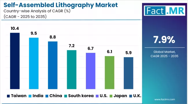
Self Assembled Lithography Market By Country | Source: Fact.MR
Japan advances self-assembled lithography through materials innovation and precision manufacturing
Japan has an efficient self-assembly lithography with the assistance of strong nanofabrication R&D, combined with the nanoscale materials sector and precision machine manufacturing industries. High-purity block copolymers and process chemicals designed to be suited to DSA and nanosphere lithography are being developed as domestic leaders in chemicals and photolithography materials.
The semiconductor industry in the country is smaller than that of Taiwan and South Korea in terms of wafer volume, but specializes in specialty logic, image sensors, and automotive-grade chips whose patterning precision is important. Process integration is a result of collaboration between the research institutes, equipment makers, and fabs. Revitalisation programs initiated by the government on semiconductors and collaborations with other chipmakers worldwide keep Japan at the centre of the market as a primary innovator.
United States leads in DSA-EUV integration and semiconductor R&D
The U.S. self-assembled lithography market has the caveat of an excellent semiconductor design ecosystem, photonics research and equipment innovation ecosystem. Top research centers and national labs are at the forefront of integrating DSA with EUV lithography to realize sub-5 nm patterning with fewer defects. Domestic semiconductor fabrication plants and foundries are experimenting with self-assembly to increase the yield of advanced logic and memory manufacturing.
2025-to-2035.webp "Us Self Assembled Lithography Market Country Value(usd Million)2025 To 2035")
Us Self Assembled Lithography Market Country Value(usd Million)2025 To 2035 | Source: Fact.MR
The materials science industry in the country facilitates the development of the next generation of resists and copolymers tailored to defect control. Domestic manufacturing capacity is being supplemented by federal grant programs such as the CHIPS Act to help improve production capacity, and collaborations between some of the largest technology companies, startups, and universities contribute towards faster commercialization of nanofabrication technologies.
South Korea leads self-assembled lithography adoption in semiconductor manufacturing.
The main driver in the self-assembled lithography industry in South Korea is the country's leadership status in memory and logic chip manufacturing, which is dominated by Samsung and SK Hynix companies. These companies are directly investing in DSA and nanosphere lithography, as scaling beyond EUV remains, and they want to further scale and increase yield and cost efficiency. There is a state of advanced in-house R&D leading to rapid prototyping and the ability to integrate new patterning techniques into mass production.
Cooperation with the local chemical suppliers also provides a local supply of high-quality block copolymers and related process materials. Vigorous government support in semiconductor leadership and strategic alliances with world equipment makers have placed South Korea ahead in the gaming semiconductor leadership. Malaysia, on the other hand is a precursor in adopting self-assembly lithography.
Category-Wise Analysis
DSA drives cost-efficient, high-precision patterning for advanced semiconductor nodes
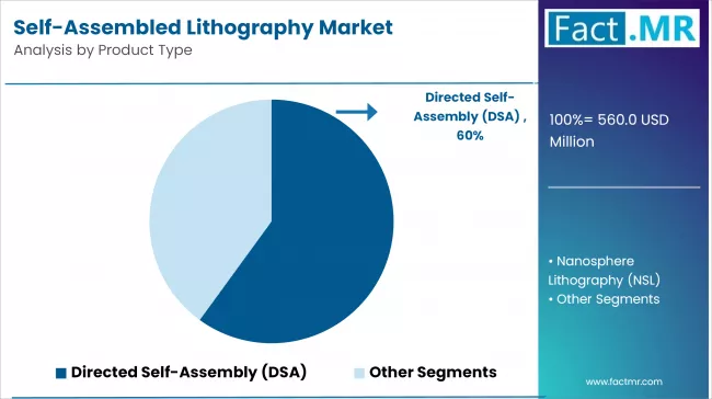
Self Assembled Lithography Market By Product Type | Source: Fact.MR
The DSA market is becoming an extremely popular segment with semiconductor fabricators demanding ultra-high-resolution patterning at low costs for sub-5 nm nodes. DSA offers excellent line-edge roughness uniformity, defect reduction, and pattern integrity relative to traditional approaches made possible by taking advantage of the block copolymer phase separation. The endorsement of EUV lithography enables its smooth incorporation with the current manufacturing process, resulting in a decrease in total capital expenditure.
Process stability and scalability are being improved by material innovation, including chemically selective BCPs. It is also in demand because it is versatile in application with logic, memory, and advanced photonics. As fabs focus on expanding Moore's Law with limited rises in the costs, the widespread use of DSA will continue to spread because of its performance-driven pull.
Self-assembled lithography boosts advanced chip yield, density, and efficiency
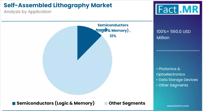
Self Assembled Lithography Market By Application | Source: Fact.MR
Self-assembled lithography is most applicable in the semiconductors segment, especially in the logic and memory devices. There is a growing need to exceed EUV limits in the development of advanced patterning in DRAM, NAND and high-performance logic. Better feature control and defect minimization lead directly to a higher chip yield and performance reliability.
Excellent process repeatability and compatibility with currently existing manufacturing implementations further enable the integration into the production line of foundries. Increased demand for AI, 5G, and data center hardware has escalated the production of high-density chips, which is likely to generate the adoption of self-assembly techniques, bringing forth cost-effective scaling and retaining proper competitive manufacturing benefits.
Self-assembled lithography boosts precision, scalability, and cost efficiency
The major adopters of self-assembled lithography are semiconductor foundries and integrated device manufacturers, who have integrated it into volume production where it can replace traditional high-precision lithography with a less costly alternative, improving the precision of their patterns along the way. The scalability of DSA and NSL advantages these players as they are not costly in terms of equipment overhaul, as they complement EUV processes.
Minimal downtimes and quick yield increase are delivered with the custom process integration. Technology readiness is being boosted by strategic partnerships and alliances with material supply and equipment suppliers. Currently, foundries specializing in high-performance logic and advanced memory are using self-assembly to achieve higher pattern density at lower cost, becoming a key competitive enabler in the overall semiconductor supply chain.
Competitive Analysis
Key players in the self-assembled lithography industry include ASML Holding N.V., Applied Materials, Inc., Tokyo Electron Limited, Lam Research Corporation, Nikon Corporation, Canon Inc., EV Group E. Thallner GmbH, Synopsys, and KLA Corporation.
The self-assembled lithography market is on the rise, with semiconductor manufacturers needing better and cost-effective technology in patterning sub-5nm nodes. The interaction between technology developers, material supply providers and equipment developers determines the competitive dynamics. Market Leaders are experimenting with high-purity block copolymers, defect-removal methods, and the combination of DSA with EUV to improve lithography yield and scalability. Developers of nanosphere lithography are looking at flexible electronics and photonics to diversify the market. Optimization of the processes is gaining pace with the strategic alliances between semiconductor foundries, research institutes, as well as the lithography equipment manufacturers. Asian-Pacific, North American and European regional specialization, together with the creation of barriers by IP, adds competitiveness and factors allowing knowledge-driven technology differentiation.
Recent Development
- In April 2025, Multi-partner (Tokyo Electron, AZ Electronic Materials and the University of Wisconsin) collaboration took a lab, scale DSA flow to fab-compatible readiness. This will facilitate the pathway between academic demonstration and the industrial conversion to DSA in semiconductor fabs through this partnership.
- In February 2025, MEC announced a high-chi blockpolymer DSA process capable of transferring a 18 nm pitch line/space in HVM-compatible conditions. At the SPIE Advanced Lithography Conference the same year, MEC announced pattern integration into a SiN layer at 18 nm pitch line/space under HVM-compatible conditions, using an improved dielectric dry-etch chemistry- a key demonstration in advancing DSA to sub-2 nm nodes.
Fact.MR has provided detailed information about the price points of key manufacturers of the Self-Assembled Lithography Market positioned across regions, sales growth, production capacity, and speculative technological expansion, in the recently published report.
Methodology and Industry Tracking Approach
The Global Self-Assembled Lithography Market is surveyed on the basis of 2025 Fact.MR report which was interviewing more than 10,200 stakeholders in 30 countries with at least 300 interviewees per market. Two-thirds were end users or operators that is to say, purchasers of equipment (e.g., semiconductor foundries, integrated device manufacturers, photonics companies) and the rest one-third, industry professionals that is to say, suppliers of equipment (e.g., materials scientists, equipment engineers, supply chain managers). Information gathering between May 2024 and April 2025 included market trends, adoption drivers, investment priorities and technical issues in the value chain. The responses were weighted in accordance with the regional capacities of production and representation of the industries. A regression analysis, coupled with more than 250 reputable sources such as patents, technical journals, regulatory filings and financial reports, worked to enhance accuracy.
With Fact.MR monitoring consumer behavior, product efficacy, industry trends, and market opportunities since 2018, this report is becoming an authoritative source of information that stakeholders can rely on.
Segmentation
Segmentation of Self-Assembled Lithography Market
-
By Technology :
- Directed Self-Assembly (DSA)
- Nanosphere Lithography (NSL)
-
By Material Type :
- Block Copolymers (BCPs)
- Colloidal Nanoparticles
- Specialty Photoresists & Etch Materials
-
By Application :
- Semiconductors (Logic & Memory)
- Photonics & Optoelectronics
- Data Storage Devices
- Flexible & Printed Electronics
-
By End-Use Industry :
- Semiconductor Foundries & IDMs
- Research Institutions & Universities
- Consumer Electronics Manufacturers
- Telecommunications
- Automotive Electronics
-
By Region :
- North America
- Latin America
- Western Europe
- Eastern Europe
- East Asia
- South Asia & Pacific
- Middle East & Africa
Frequently Asked Questions
What was the Global Self-Assembled Lithography Market Size Reported by Fact.MR for 2025?
Who are the Major Players Operating in the Self-Assembled Lithography Market?
What is the Estimated Valuation of the Self-Assembled Lithography Market in 2035?
What Value CAGR did the Self-Assembled Lithography Market Exhibit Over the Last Five Years?
Who worked on this report


Preview the report firsthand - request a free sample
Free SampleGet the brochure for pricing and purchase details
Download PDF