- Base Value(2025): 1798 Mn
- Forecast Value (2035): 8280 Mn
- CAGR (2035): 16.3%
Nanosheet FETs Market Outlook 2025 to 2035
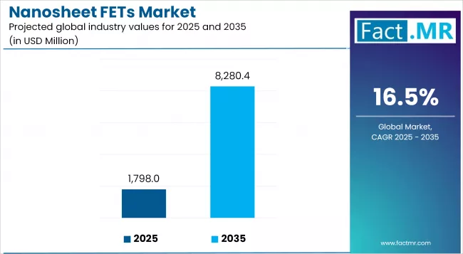
The global Nanosheet FETs market is expected to reach USD 8,280 million by 2035, up from USD 1,798 million in 2025. During the forecast period 2025 to 2035, the industry is projected to expand at a CAGR of 16.5%.
Nanosheet FETs market is experiencing a high growth rate due to the shift of semiconductor industry beyond FinFET technology to facilitate advanced node scale below 5nm. Increasing usage of high-performance computers, AI accelerators and energy efficient mobile processors is driving adoption. Important motivation factors are enhanced electrostatic control, increased drive current and enhanced power efficiency of nanosheet architectures.
The commercialization is accelerating with Samsung, TSMC and Intel investing in nanosheet based GAAFET nodes. Besides, the need to use EUV lithography instruments, design enablement and heterogeneous integration is creating growth in the ecosystems, making nanosheet FETs a pillar of the next generation logic devices.
Quick Stats for Nanosheet FETs Market
- Industry Value (2025): USD 1,798 Million
- Projected Value (2035): USD 8,280 Million
- Forecast CAGR (2025 to 2035): 16.5%
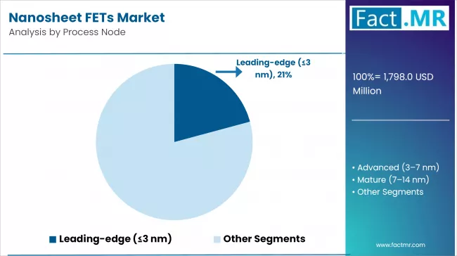
- Leading Segment (2025): Advanced (3–7 nm) (38.2%Market Share)
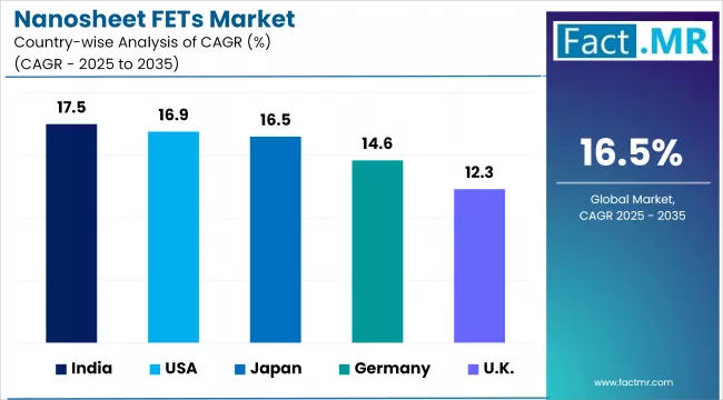
- Fastest Growing Country (2025-2035): India (17.5% CAGR)
- Top Key Players: Samsung Electronics, TSMC, Intel, IBM, and GlobalFoundries
Nanosheet Fets Market Industry Value Analysis | Source: Fact.MR
What are the drivers of the Nanosheet FETs market?
The nanosheet FETs market is registering a healthy growth because the semiconductor industry is in the effort of going beyond the constraints of the FinFET technology and continue to scale its transistors further on its advanced nodes. Nanosheet FETs offer better electrostatic control, minimized short-channel effects, and allowed higher drive-currents, thus being essential in the realisation of 3 nm and 2 nm process nodes and enhanced performance and power efficiency.
The adoption is being driven by the increase in demand of high-performance and energy efficient chips in data centers, artificial intelligence, machine learning, and 5G applications. Nanosheet FETs have a better performance-per-watt ratio, which makes them an ideal candidate in the next-generation CPUs, GPUs and mobile SoCs that need to be optimized in terms of power consumption without the need to compromise processing capacity.
The continuous investment by the world semiconductor leaders and foundry is also serving to speed up technology development and commercialization. The supply chain is being made more robust with strategic partnerships with the equipment manufacturers, the material suppliers and vendors of the EDA tools so that the costs are pushed down and the nanosheet-based devices can be deployed at large scale.
What are the regional trends of the Nanosheet FETs market?
The regional trends of the nanosheet FETs market are characterized by the adoption depending on the semiconductor manufacturing and the R&D centers of the world.
In East Asia, the shift to nanosheet-based nanosystems is being spearheaded by countries that are also dominating the fabrication of wafer, advanced foundries as well as strong government backing on innovation of semiconductors.
North America has been one of the major contributors having impressive investments in R&D, design enablement, and early adopter by built-in device manufacturers and fabricless firms specializing in AI and high-performance computer.
Western Europe is an important contributor with sophisticated equipment and material provision, which facilitates the manufacture of nanosheets worldwide and promotes the development of new process technologies.
In the meantime, South Asia and the Pacific is becoming an important player, drawing new fab investment and developing design and packaging capability to help with the technology transition.
Latin America, the Middle East and Africa are lagging behind, yet are experiencing slowing interest as global supply chains diversify and semiconductor production moves geographically.
What are the challenges and restraining factors of the Nanosheet FETs market?
The nanosheet FETs market has a number of challenges and limiting factors, which may restrain its adoption rate. A significant issue is that nanosheet transistors are very expensive and difficult to fabricate and would require high-level lithography, process control, and capital-intensive development. The move to nanosheet FETs over FinFETs will require retooling of facilities, new process design packages, and significant validation and extends time-to-market and total costs to semiconductor companies.
The other important constraint is the technological challenge in maintaining high yield rates at advanced nodes. Nanosheet FET manufacturing implies small dimensional control, variation control, and integration issues using new generation materials. Losses of yield may seriously affect profitability, where smaller foundries would find it difficult to struggle.
Also, there are supply chain risks involving ecosystem dependence on EUV lithography tools and special equipment. The lack of access to important manufacturing equipment and absence of workforce can slow down the capacity growth and postpone the mass commercialization.
Country-Wise Insights
Nanosheet Fets Market Cagr Analysis By Country | Source: Fact.MR
India is Emerging as a Strategic Hub for Nanosheet FETs Design and Ecosystem Development
India is also making efforts to emerge as a key player in the nanosheet FETs market globally by enhancing its role in semiconductor design, research, and development, and supporting ecosystem. Although large-scale wafer production is at an early phase, India is developing major strengths in chip design, verification, and EDA tool development, which are needed to implement nanosheet FETs. With the semiconductor incentive programs and collaboration with international foundries, the government is establishing the infrastructure of domestic manufacturing in the future.
The increasing and emerging talent of semiconductor engineers in India is also catching the interest of the largest players in the market to establish R&D centers dedicated to advanced node designs and enablement of nanosheet technology. The cooperation between academia, startups and international semiconductor leaders is rapidly developing IPs and getting the nation ready to transition to next-generation technologies. The above steps put India as a strategic location to aid global nanosheet FET deployment and innovation.
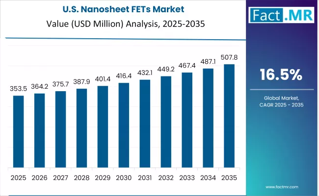
The United States is Driving Innovation and Early Adoption of Nanosheet FETs for Next-Generation Semiconductor Solutions
The United States is taking a leading role in driving the nanosheet FET technology by heavily investing in the research and development, and the enabling of design. The major integrated device vendors and fabless firms are seriously considering stacked nanosheet and GAAFET designs to improve the performance, power consumption, and scalability of next-generation processors.
The U.S. semiconductor ecosystem is blessed with the state-of-the-art R&D centers, engineering expertise, and a strong network of EDA tools vendors, equipment manufacturers, and material suppliers, all of which help commercialize nanosheet-based devices.
Nanosheet Fets Market Country Value Analysis | Source: Fact.MR
These high-performance computing, AI accelerators, and 5G infrastructure are the areas where energy-efficient and high-speed transistors are needed, and therefore, early adoption. The empowerment of the U.S. position can further be enhanced by the government initiatives, strategic partnerships, and incentives of domestic semiconductor manufacturing, which makes it a key centre in innovation and technological leadership in the global nanosheet FET market.
Japan is Driving Innovation in Nanosheet FETs Through Advanced Materials and Equipment Expertise
The importance of Japan in the global nanosheet FETs market is through its dominance in semiconductor equipment, precision materials and process technologies. Although the country is not at the forefront in terms of large-scale production of logic chips, it makes major contributions in terms of advanced lithography, deposition and etching equipment and high quality of wafers that make possible the manufacture of nanosheet transistors all over the world.
Japanese companies are also working closely with the foundries and integrated devices manufacturers to refine the nanosheet processes and increase the performance and reliability of the devices. Research and development especially in the materials engineering area of the country contribute towards enhancing channel mobility and transistor efficiency that is essential in nanosheet FET scaling.
In addition, Japan has been able to implement a well-established semiconductor supply chain, which has guaranteed uniform quality and innovation in manufacturing support, including metrology systems to specialty chemicals. These capabilities make Japan the key node of adoption and commercialization of next-generation nanosheet FET technologies.
Category-Wise Analysis
Advanced Nodes are the Heart of Performance-Driven Nanosheet FET Adoption
Nanosheet Fets Market Analysis By Process Node | Source: Fact.MR
The 3-7 nm node is an advanced node that is strategically important in making the nanosheet FET technology a reality, between the state-of-the-art leading-edge nodes and the mainstream semiconductor processes. The nodes are essential to provide better power efficiency, higher drive currents, and overall performance, which makes them very appropriate to mainstream applications such as high-performance processors, AI accelerators, and mobile SoCs. Such a level of adoption enables semiconductor companies to utilize nanosheet architectures without extreme costs and technical risk of sub-3 nm nodes and allows a trade-off between performance improvement and manufacturing.
The ecosystem is being fortified with leading foundries and IDMs having a growing investment in process optimization, design enablement and tool development in the advanced nodes. Consequently, the 3-7 nm segment is becoming the driving force behind the commercialization of nanosheet FETs and making them a viable solution to commercial next generation computing using nanosheet FETs.
Battery Manufacturing is Driving Closed-Loop Scrap Integration
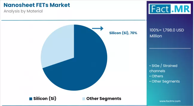
Nanosheet Fets Market Analysis By Material | Source: Fact.MR
Silicon is still the material of choice in nanosheet FETs, and is the cornerstone of new transistor technology. It has superior electrical characteristics, is inexpensive, and has established processing methods that have made it the material of choice when manufacturing nanosheet architectures at large scale. Silicon nanosheets are seen to control electrostatics better, yielding reduced short channel effects and better drive currents than conventional FinFETs. The compatibility of the material with current CMOS processes will make transition to nanosheet technology in fabs easier whilst reducing production risk and costs.
Also, thermal stability and reliability of silicon have been used in high-performance applications in CPUs, GPUs, AI accelerators, and mobile SoCs. Although other materials such as SiGe and compound semiconductors are under consideration to achieve higher mobility, silicon is still dominant as it is matured, scalable and has a wide ecosystem of foundries, equipment manufacturers and design tool suppliers. Its application is vital towards the production of next-generation electronics at reduced costs and with high efficiency.
Competitive Analysis
Key players in the Nanosheet FETs market Samsung Electronics, TSMC, Intel, IBM, GlobalFoundries, SK hynix, Micron Technology, UMC (United Microelectronics Corporation), SMIC (Semiconductor Manufacturing International Corp.), ASML Holding, Applied Materials, Inc., Lam Research Corporation, Tokyo Electron Ltd. (TEL), KLA Corporation, Synopsys, Inc.
Nanosheet FETs market is faced with high competition due to the high rate of technological development and the demand of next generation of transistor architectures. Firms are working on new process technology, devices, and materials towards the realization of smaller nodes, higher performance, and energy efficiency. Constant research and development, pilot production and ecosystem collaborations are among the major strategies to stay competitive.
Competition in the market also exists in terms of securing advanced fabrication equipment, devising powerful design enablement tools and optimizing yield at advanced nodes. Also, intellectual property, proprietary manufacturing procedure and quality supply chain management differentiation make significant contributions to market position sustenance. With the industry changing, companies need to strike a balance between cost-saving and leading-edge technology to fulfill the increasing demand of high-performance computing, AI accelerators, mobile SoCs, and new uses, and agility, technological leadership, and collaboration should be the key to long-term success in the nanosheet FETs market.
Recent Development
- In December 2024, TSMC described its next-generation transistor technology at the IEEE International Electron Device Meeting (IEDM) in San Francisco. The N2, or 2-nanometer, technology is the semiconductor foundry giant’s first foray into a new transistor architecture, called nanosheet or gate-all-around. Samsung has a process for manufacturing similar devices, and both Intel and TSMC expect to be producing them in 2025.
Fact.MR has provided detailed information about the price points of key manufacturers of Nanosheet FETs Market positioned across regions, sales growth, production capacity, and speculative technological expansion, in the recently published report.
Methodology and Industry Tracking Approach
According to Fact.MR, the global Nanosheet FETs market report of 2025 relies on the results of the research conducted in 12 countries out of which 1,200 stakeholders gave at least seven hundred and fifty-five responses. Sixty-five percent of these participants were end users (seminductor manufacturers, device OEMs, telecom equipment providers, and R&D heads) and the other 35% were supply chain managers, environmental compliance consultants, and technology policy advisors.
The fieldwork was performed during the time period of July 2024, June 2025; the main parameters involved were efficiency of performance of the devices, ability of integration of the processes, compliance with the regulations, scalability of manufacturing, and cross-border trade of the components. The use of a balanced calibration model was to guarantee proper representation of the regions throughout North America, Europe, and Asia.
Over 95 credible sources, such as semiconductor industry reports, foundry and fab audits, technology adoption surveys, patent filings and logistics optimization datasets were leveraged by the study. Triangulation protocols have been used, which have facilitated a high data reliability level, which will give accurate predictions and actionable information to the stakeholders in the Nanosheet FET ecosystem.
Fact.MR employed sophisticated methods of data analysis, such as multi-variable regression analysis and scenario modeling, to ensure that data have been robust. As the advanced semiconductor space has been monitored since 2018, this report features a detailed roadmap to companies seeking to achieve innovation, competitive edge, and sustainable development in the Nanosheet FET market.
Segmentation
Segmentation of Nanosheet FETs Market
-
By Process Node :
- Leading-edge (≤3 nm)
- Advanced (3-7 nm)
- Mature (7-14 nm)
- Legacy (>14 nm
-
By Material :
- Silicon (Si)
- SiGe / Strained channels
- Others
-
By Application :
- Consumer Electronics
- High-Performance Computing (HPC) & Data Centers
- Automotive
- Internet of Things (IoT) & Edge Devices
- Telecommunications
- Others
-
By End-use Industry :
- Semiconductor Foundries
- Integrated Device Manufacturers (IDMs)
- Fabless Semiconductor Companies
- Original Equipment Manufacturers (OEMs)
- Others
-
By Region :
- North America
- Latin America
- Western Europe
- Eastern Europe
- East Asia
- South Asia & Pacific
- Middle East & Africa
Frequently Asked Questions
What was the Global Nanosheet FETs Market Size Reported by Fact.MR for 2025?
Who are the Major Players Operating in the Nanosheet FETs Market?
What is the Estimated Valuation of the Nanosheet FETs Market in 2035?
What Value CAGR did the Nanosheet FETs Market Exhibit Over the Last Five Years?
Who worked on this report


Preview the report firsthand - request a free sample
Free SampleGet the brochure for pricing and purchase details
Download PDF